Article

Design of Efficient Concurrent Dual-Frequency Doherty Power Amplifier Based on Step Impedance Low-Pass Filter

School of Electronic and Information Engineering, Liaoning Technical University, Huludao 125100, China
*
Author to whom correspondence should be addressed.
Electronics 2023, 12(19), 4092; https://doi.org/10.3390/electronics12194092
Submission received: 4 September 2023 / Revised: 16 September 2023 / Accepted: 20 September 2023 / Published: 29 September 2023
(This article belongs to the Special Issue Recent Advances in Microwave and Terahertz Engineering)

Abstract

:
In view of the peak-to-average power ratio (PAPR) of wireless communication base stations, a Doherty power amplifier with high efficiency maintained at output power back-off (OBO) can effectively solve the problem of low efficiency of the traditional power amplifier at the point of power back-off. In this paper, we propose a method to implement a dual-frequency Doherty power amplifier (DPA) using a step-impedance low-pass filter to improve the bandwidth and efficiency of the DPA at output power back-off (OBO). Step impedance low-pass filters are used to solve the bandwidth limitations in traditional impedance converters and improve the efficiency of Doherty power amplifiers to a certain extent. In order to verify the proposed scheme, an efficient concurrent dual-band Doherty power amplifier operating at 2.0/3.5 GHz is designed and fabricated for the first range 1 (FR1) of 5G applications. In the measured results, the concurrent dual-band DPA achieves a saturated output power of 44 dBm and drain efficiency of 62% with a 6 dB back-off efficiency of 53% at 2.0 GHz and a saturated output power of 43.5 dBm and drain efficiency of 68% with a 6 dB back-off efficiency of 58% at 3.5 GHz.

1. Introduction

With the increase in the communication rate [1], the demand for communication capacity at the base station increases; therefore, high spectrum efficiency and high data rate orthogonal frequency division multiplexing (OFDM) signals [2] are one of the main modulation signals used today. Since OFDM signals are composed of multiple independently modulated subcarrier signals superimposed on each other, when the phases are the same, the superimposed signals tend to generate large instantaneous power peaks, resulting in a high peak-to-average power ratio (PAPR). This modulating signal tends to enter the nonlinear region of the power amplifier, and in order to avoid large distortion, the power amplifier is generally operated at the output power back-off point. Traditional power amplifiers have low power-added efficiency (PAE) at the output power back-off (OBO), resulting in large energy loss. The Doherty power amplifier (DPA) is based on the principle of active load modulation [3] to maintain high efficiency at OBO. A concurrent multi-band Doherty power amplifier [4,5] can achieve a reasonable allocation of spectrum resources and reduce interference to adjacent channel signals. Compared with the traditional multi-channel single-frequency power amplifier, the concurrent dual-band Doherty design structure can also effectively reduce system size and cost as well as have good back-off efficiency [6].
In 2012, Rawat et al. [7] used a T-type or π-type network structure to implement concurrent dual-frequency Doherty power amplifiers. The conventional quarter-wavelength impedance converter is replaced by a T-type or π-type structure and is equivalent in both frequency bands at the same time. Through the derivation of theory and formula, the solution is verified mathematically. However, the whole solution process is complicated and involves solving transcendental equations, and the result of the solution may not conform to the physical size, such as the negative solution. In this regard, Rawat et al. gave another solution by adding a T-shaped structure to match the impedance value to a transition impedance value, i.e., a one-step impedance matching process is divided into a two-step transformation to 50 Ω, which has similarities with the principle of step impedance matching. In 2012, Paul et al. [8] designed a dual-frequency Doherty power amplifier operating at 1.8 GHz and 2.4 GHz using the theory of harmonic suppression, and its efficiency in the power back-off region reached 60% and 44%, respectively. In 2016, Songbai He’s team at the University of Electronic Science and Technology of China [9] designed a dual-band Doherty power amplifier by using the transistor’s parasitic parameters directly as part of the impedance transformation and achieved 63% and 51% power back-off point efficiencies at 1.8 GHz and 2.6 GHz, respectively. In 2016, Serkan and Ahmet, University of Issyk-Kul, applied the real frequency technique to the design of dual-band matching networks [10]. The real frequency technique was used to synthesize a matching network with the dual-band response of a bandpass prototype while combining low-pass (LP) and high-pass (HP) sections in a cascade and optimizing under LP and HP frequency transformation. Finally, the dual-band matching network has 300 MHz and 500 MHz bandwidth at 1 GHz and 2 GHz, respectively. In 2016, Prof. S. Boumaiza’s group at the University of Waterloo [11], Canada, implemented a concurrent dual-band Doherty amplifier with a 300 MHz bandwidth by improving the π-shaped output combining network. In the same year, Alessandro Cidronali et al. [12] proposed a new method of compensated impedance inverters for absorbing the output capacitance and extending the DPA bandwidth by introducing a half-wavelength transmission line as an offset line in the peak amplifier branch. In 2020, it was mentioned in reference [13] that a phase–period matching network can be used as a multi-band impedance inverter, bias element, and phase compensator to realize a multi-band Doherty power amplifier. A six-band dual-mode Doherty power amplifier is finally realized by using reciprocal gate bias in the same way as the reference [14]. In one of these modes, the dual-frequency Doherty amplifier can obtain a bandwidth of 400 MHz. For high PAPR multi-band system applications, broadband DPAs and dual-band DPAs [15,16,17,18,19,20,21] are widely used.
Although the above studies provide good solutions for the design of concurrent dual-band Doherty amplifiers, the structure and calculation are complicated. In order to further simplify the design difficulty and extend the dual-band bandwidth, in this paper, we propose a method to realize a dual-band Doherty power amplifier using a step-impedance low-pass filter. A conventional Doherty power amplifier consists of a combination of a carrier power amplifier and a peak power amplifier. As shown in Figure 1, the input power is split in two by a Wilkinson power divider, and both the carrier and peak power amplifiers are connected with phase compensation lines used to achieve phase alignment of the signals from the carrier and peak power amplifiers as well as an open-circuit state for the peak power amplifier. The impedance matching at the junction point is achieved through an impedance converter. In this paper, we propose an efficient dual-band DPA to achieve dual-band matching by employing a fourth-order step impedance filter in the input and output matching network and post-matching network. Step impedance filters are simple and easy to implement and can be used as low-pass filters, as well as dual-band, matched networks. Due to the broadband matching characteristics of the step impedance low-pass filter, the operating bandwidth of the dual-frequency can be effectively extended, which can meet the multi-frequency and multi-standard requirements of the current communication system well. Finally, in this paper, a concurrent dual-band Doherty power amplifier operating at 2.0/3.5 GHz for FR1 of 5G applications is designed, with good results.

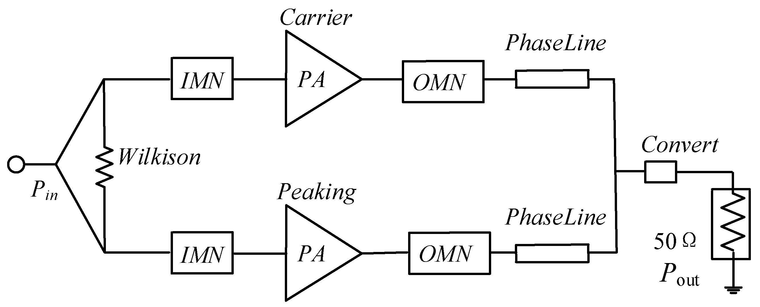
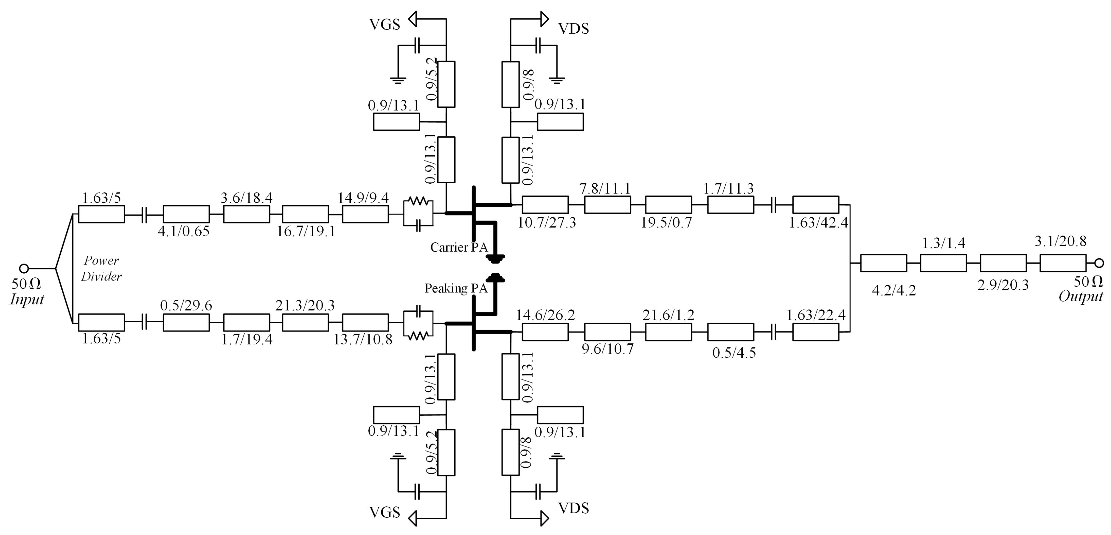
2. Design of Concurrent Dual-Band Doherty Power Amplifier

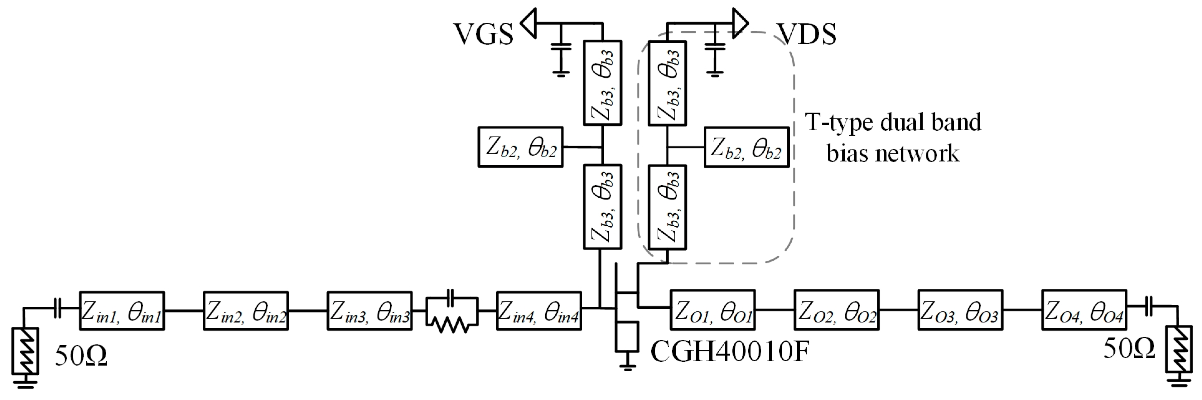
2.1. Design of Carrier Power Amplifier

The Doherty power amplifier consists of a carrier power amplifier and a peak power amplifier. The carrier power amplifier is designed first. The step impedance filter uses alternating microstrip lines of high or low characteristic impedance, which allows broadband impedance matching as well as dual-frequency point matching. The carrier power amplifier uses a fourth-order step impedance filter structure for both input matching and output matching. In particular, the output matching network achieves 50 Ω at output power saturation and 25 Ω impedance matching at 3 dB back-off.
The traditional design method is to first determine the fourth-order low-pass filter to be designed by using the design table and then calculate the required parameters of the bandpass filter based on the formula conversion. A microstrip filter design is usually a prototype circuit design method based on a comprehensive design. The prototype circuit is a low-frequency lumped circuit with inductors and capacitors as components, as shown in Figure 2. In the actual process, the prototype circuit parameters can be converted to the actual filter component values according to the filter design index requirements and according to certain transformation relations. The specifications of the designed filter are shown below.
The cut-off frequency is fc = 2 GHz; the passband maximum attenuation is Lar = 0.2 dB; the stopband side frequency is fs = 4 GHz; and the stopband minimum attenuation is Las = 34 dB.
The characteristic impedance of the input and output transmission lines is Zc = 50 Ω, the relative permittivity of the microstrip substrate material is ε = 3.66, and the substrate thickness is h = 0.762 mm.
There are several filter design models, such as the Butterwolf prototype filter, elliptic function filter, Chebyshev filter, and so on. In this paper, the Chebyshev filter is used; firstly, the order of the filter is determined (selected equal ripple waveforms and capacitive input ladder network) and calculated as follows:
(1) The normalized frequency is calculated as follows:
Q = fs/fc = 4/2
Take the filter order N = 5.
(2) When Lar = 0.2 dB, the normalized value of the equal-ripple low-pass filter element is g1 = g5 = 1.3394; g2 = g4 = 1.3370; g3 = 2.1660; and g6 is equal to 1. The L and C low-pass filter circuits designed in this paper are shown in Figure 2.
Using a capacitive input ladder network, the real values of each component in the figure are calculated as follows:
C 1 = C 5 = g 1 / 2 π f c Z c
C 3 = g 3 / 2 π f c Z c
L 2 = L 4 = g 2 Z c / 2 π f c
In the process of calculating the structural size of the filter, there are generally the following requirements for the selected high- or low-impedance transmission line:
Z o h g L Z c π / 4
Z o L π Z c 4 g c
Zoh is the calculated characteristic impedance of the high-impedance line when the high-impedance line is selected as the transmission line, and ZoL is the calculated characteristic impedance of the low-impedance line. In the actual selection process, Zoh = 100 is generally the best choice for the high-impedance line if the selected low microstrip line is too long or if the selected high microstrip line is too fine and difficult to process. Finally, the pahse constant of the high-impedance line is Zoh = 101 Ω, that of the low-impedance line is ZoL = 10 Ω. β is the phase constant in this paper.
For a high-impedance line, when ε r = 3.66 and Z c = 101   Ω , one can obtain w/h = 0.1 and the following relationship:
λ / λ T E M = 1.28
λ T E M = λ 0 ε r
λ = λ g = λ 0 ε r e
After derivation, one obtains
λ g = 1.28 λ T E M = 1.28 λ 0 ε r
ε r e = λ 0 λ g 2
Thus, the phase velocity of the high-impedance line and the high-impedance line length can be derived as
V p h = c ε r e
l 2 = l 4 = V p h L 2 Z c
Similarly, for low-impedance lines, when ε r = 3.66 and Z c = 10 Ω, there is the following relationship: w/h = 10 and λ / λ T E M = 1.08 , so the calculation formula is as follows:
ε re = λ 0 λ 2 = λ 0 1.08 λ TEM 2 = ε r 1.08 2
And, V P L = c ε r e low-impedance line length is as follows:
l 1 = l 5 = V P L C 1 Z c
l 3 = V P L C 3 Z c
For the width of the microstrip line, the width and length of the actual microstrip line are calculated based on the impedance and the required electrical length using the microstrip line calculator tool, where the input and output microstrip line characteristic impedance is Zc = 50 Ω. Parameters are determined by low-pass filter prototyping and finally simulated by ADS. The amplitude–frequency response and S-parameters of the microstrip line filter are simulated using ADS to analyze whether the performance of the microstrip filter reaches the design specifications, and the microstrip line parameters are adjusted accordingly.
The step impedance low-pass microstrip filter is shown in Figure 3. Step-impedance converters can realize impedance conversion in the wide band range, and in this paper, a step impedance converter is chosen to implement the input and output matching networks, as well as the impedance conversion at the merging point. The step impedance converter has a similar structure to the impedance filter and can realize the transition from 25 Ω to 50 Ω at saturation output power and OBO The bandwidth limitation of the traditional quarter-wavelength impedance converter is solved.
The RF bias circuit is the direct current circuit of the power amplifier that isolates AC and conducts DC as a way to protect the DC power supply. In order to bring the gate and drain input impedances to infinity, a T-type dual-frequency bias circuit is used based on the equivalent quarter-wavelength methodology, as described in reference [22]. Additionally, the gate bias is connected in series with a 28 Ω resistor to limit the gate bias current, thus protecting the transistor from being burned due to excessive current flow. Large 10 uf, medium 100 nf, and small 16 pf capacitors are connected in parallel to the gate and drain power ports to filter out spurious signals at various frequencies.
The carrier power amplifier operates in two frequency bands, 2.0 GHz/3.5 GHz, and the overall circuit is shown in Figure 4. Both the input and output matching networks use a step impedance filter structure, and the gate and drain are both T-type dual-band bias circuits. In addition, in the 3.5 GHz band, the saturated output power reaches about 41 dBm, and the efficiency reaches about 70%; at this time, the matching impedance value is 50 Ω; back off 3 dB output power, the efficiency reaches about 60%, at this time the matching impedance value is 25 Ω, so that a quarter-wavelength impedance converter can be eliminated, and also can avoid bandwidth limitation, and the same is true in the 2 GHz band. The CGH40010F transistor is not stable in the full frequency band, and in order to prevent self-excited oscillations, there have been some research results, such as the Rollett approach and the Nyquist method in the stability network in reference [23], which achieves good results in preventing self-excited oscillations caused by parallel two-way power amplifiers in Doherty mode. In order to simplify the design approach, in this paper, the RC parallel network is added to the input matching network to improve the stability of the overall circuit and prevent the transistors from being damaged due to self-excited oscillations.
The simulation results of the carrier power amplifier are shown in Figure 5. When the input power is set to 29 dBm, the output power in the 3.4–3.6 GHz band reaches 40.1–40.4 dBm, and the power additive efficiency is 64–72%; when the output power in the 1.9–2.1 GHz band reaches 40.5–41.3 dBm, the power additive efficiency is 60–66%.

2.2. Design of Peak Power Amplifier

The Doherty Power Amplifier is based on the active load principle, and the concurrent dual-band DPA is designed as a symmetrical power amplifier with the same overall circuit structure for the carrier and peak power amplifiers. During power fallback, the peak power amplifier needs to be open at the merge point to prevent the signal from the carrier power amplifier from being transmitted to the peak power amplifier. The designed concurrent dual-band Doherty power amplifier adds a section of microstrip line with a characteristic impedance of 50 Ω behind the isolation capacitor at the output of the peak power amplifier and adjusts the phase of the voltage by adjusting the length of the microstrip line, so as to make the output port present an open-circuit state in two frequency bands during power fallback. As shown in Figure 6, the output port is shown to be open-circuit in both frequency bands at OBO.
Due to the difference in certain parameters (e.g., gate voltage, input power, etc.) between the carrier power amplifier and the peak power amplifier, the phase of the output signal will change. In order to increase the output power, it is necessary to add a piece of microstrip line with a characteristic impedance of 50 Ω to the output port of the carrier power amplifier, and by adjusting the length of the microstrip line, it makes the two signals have the same phase in the two frequency bands. As shown in Figure 7a,b are the resultant plots of the phase of the output signals of the carrier and peak power amplifiers in the 3.4–3.6 GHz and 1.9–2.1 GHz bands, respectively. As can be seen from the plots, the curves of the signal phases of the peak power amplifier and the carrier power amplifier basically coincide in the two frequency bands.
As shown in Figure 8, the saturated output power of the peak power amplifier at 3.4–3.6 GHz is 40–41 dBm, with a drain efficiency of 54–65%. At 1.9–2.1 GHz, the saturated output power is 40–40.2 dBm, and drain efficiency is 50–61%. The drain and gate voltages of the peak power amplifier are 28 V and −5.4 V, respectively, and the input power is 29 dBm. The drain and gate voltages of the peak power amplifier and carrier power amplifier and the saturated output power of the peak power amplifier basically reach the same level; the power additive efficiencies all reach more than 50%, and the subsequent overall circuits have to be adjusted and optimized.

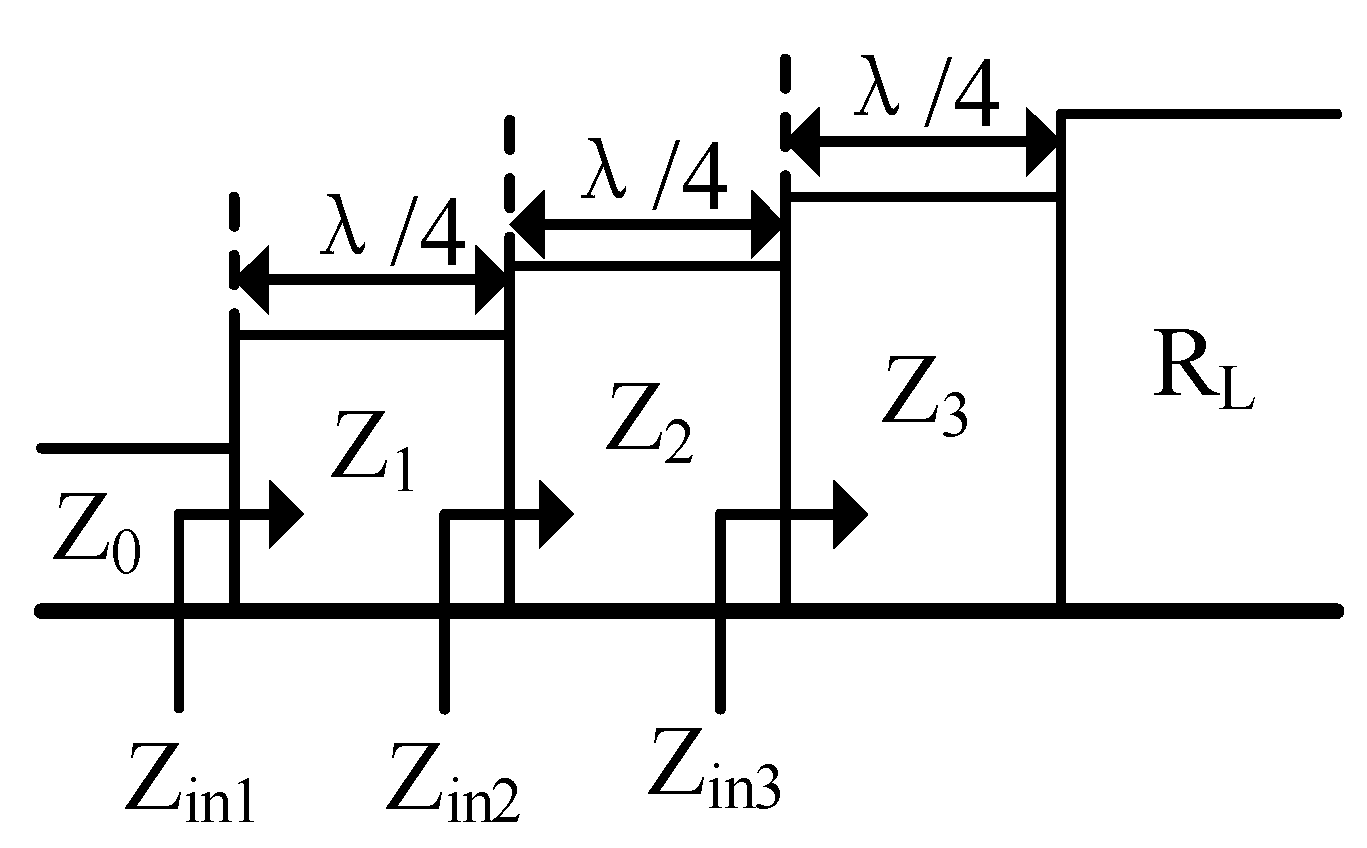
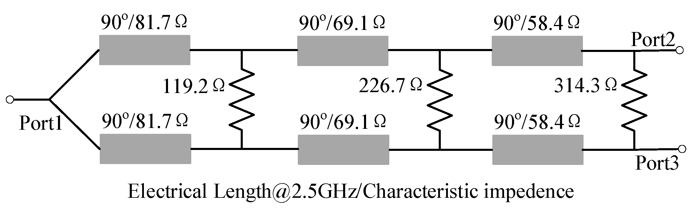
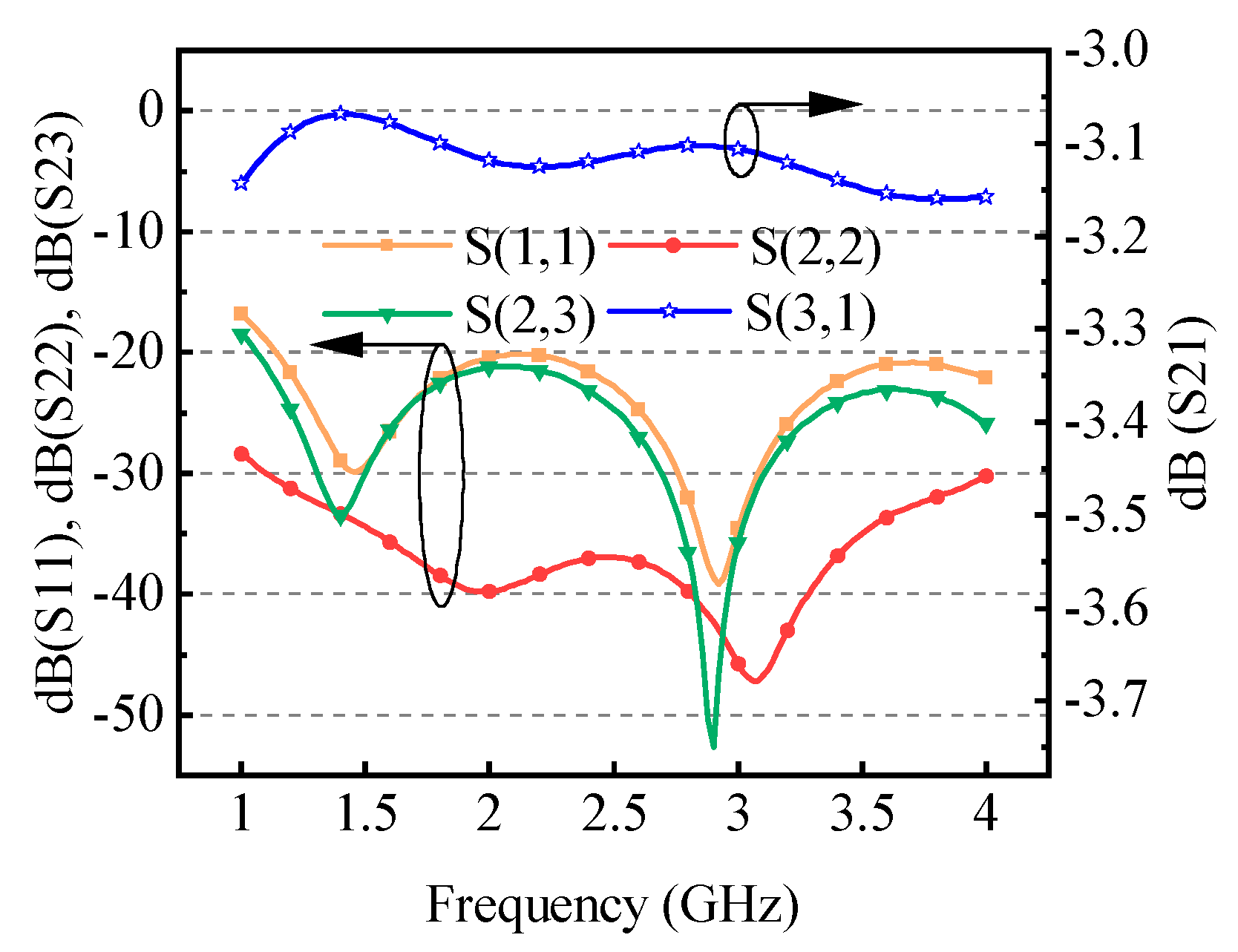
3. Broadband Wilkinson Power Divider

Typically, the input port of a Doherty power amplifier requires a power splitter to split the input power in half. The bandwidth of an ordinary Wilkinson splitter cannot meet most of the engineering applications, so widening the bandwidth of the power splitter became the focus of current research. So far, the method of bandwidth expansion by multilevel impedance conversion has been widely used in the design of power dividers. Due to the multi-stage impedance converter having a lot of small amplitude and different phase reflected waves, the reflected waves can be suppressed when superimposed so that the bandwidth can be broadened. The power divider designed in this paper is to broaden the bandwidth by cascading three levels of λ/4 step impedance converters, which is shown schematically in Figure 9.
In this paper, a Chebyshev impedance converter is used to implement the bandwidth extension of the Wilkinson power divider. The Chebyshev polynomial can be expressed as
T n x = 2 · T n - 1 x T n - 2 x
Let x = c o s θ , where |x|< 1; then, the Chebyshev polynomial can be expressed as follows:
T n cos θ = cos ( n θ )
To make the response of Equation (18) have equal ripples, it is necessary to replace c o s θ with c o s θ / c o s θ m , where θ m and π θ m are the upper and lower frequencies of the passband, respectively. Then, the above equation can be written as
T n c o s θ c o s θ n = T n s e c θ n c o s θ = c o s n a r c c o s c o s θ c o s θ m
The total reflection coefficient of the converter can be obtained by making Γ θ proportional to the passband of the Chebyshev equal ripple and combining it with Equation (19).
Γ θ = 2 e j n θ Γ 0 c o s N θ + Γ 1 c o s N 2 θ + + Γ n c o s N 2 n + = A e j N θ T N s e c θ m c o s θ
The last term of the formula obtained in Equation (20) is 1 2 Γ N / 2 when N is even, and Γ N 1 / 2 c o s θ when N is odd, where Γ 0 , Γ 1 , Γ 2 , Γ 3 are the amplitude of the reflection coefficient at the impedance gradient point. A is an undetermined constant, so θ = 0 can be obtained as follows:
A = R L Z 0 R L + Z 0 · 1 T N s e c θ m
If the amplitude of the maximum allowable reflection coefficient in the passband is Γ m , then we can obtain Γ m = A from Equation (20), because in the passband for θ m < θ < π θ m there is s e c θ m c o s θ < 1 , So there is s e c θ m c o s θ 1 in the same range.
The following can be derived:
T N sec θ m = 1 Γ m R L Z 0 R L + Z 0 1 2 Γ m ln R L Z 0
s e c θ m = c o s h 1 N a r c o s h l n R L / Z 0 2 Γ m
Γ n = 1 2 l n Z n + 1 Z n
An ultra-wideband Wilkinson power splitter composed of a third-order Wilkinson power splitter is designed. Then, the impedance of each level is calculated, and N = 3 is substituted into Equation (20) to obtain the following:
Γ θ = 2 e j 3 θ Γ 0 c o s 3 θ + Γ 1 c o s θ = A e j 3 θ T 3 s e c θ m c o s θ
The following is obtained by A = Γ m = 0.1 :
s e c θ m = c o s h 1 N a r c o s h l n R L / Z 0 2 Γ m = cos h 1 3 arcosh ln 100 / 50 2 × 0.1 = 1.21
Since c o s n θ can be expanded as the sum of polynomials of the form c o s n 2 m θ , it follows from Equation (19) when n = 3:
T 3 s e c θ m c o s θ = s e c 3 θ m c o s 3 θ + 3 c o s θ 3 s e c θ m c o s θ
The following is further available:
2 Γ 0 c o s 3 θ + Γ 1 c o s θ = A s e c 3 θ m c o s 3 θ + 3 c o s θ 3 A s e c θ m c o s θ
It can be solved through Equation (28) that Γ 0 = 0.0886 , Γ 1 = 0.0842 . According to the symmetry, Γ 2 = Γ 1 , Γ 3 = Γ 0 , and substituting the value of Γ 0 , Γ 1 , Γ 2 , Γ 3 into Equation (24) can calculate Z1 = 81.7 Ω, Z2 = 69.1 Ω, and Z3 = 58.4 Ω. The calculation of the isolation resistance is overly complicated and can be obtained by consulting the table: R1 = 119.2 Ω, R2 = 226.7 Ω, and R3 = 314.3 Ω.
The calculation of all key parameters of the Wilkinson power divider is completed, as shown in Figure 10.
The simulation results of the designed broadband Wilkinson power amplifier are shown in Figure 11, and S11 is less than −20 dB in both 1–4 GHz bands, which satisfies the radiation coefficient requirement at the input port. S22 is less than −25 dB in the 1–4 GHz band and also satisfies the reflection coefficient requirement of the output port, and S33 and S22 have the same index because of the symmetrical structure. S23 is less than −23 dB in the 1–4 GHz band, which basically meets the isolation requirement between port 2 and port 3. S21 is −3.1 dB in the 1–4 GHz band, which shows that the output power of port 2 is 1/2 of the input power of port 1. In the same way, since the Wilkinson power divider is a symmetrical structure, the output power of port 3 is 1/2 of the input power of port 1. All the specifications of the designed broadband Wilkinson power divider satisfy the design requirements.

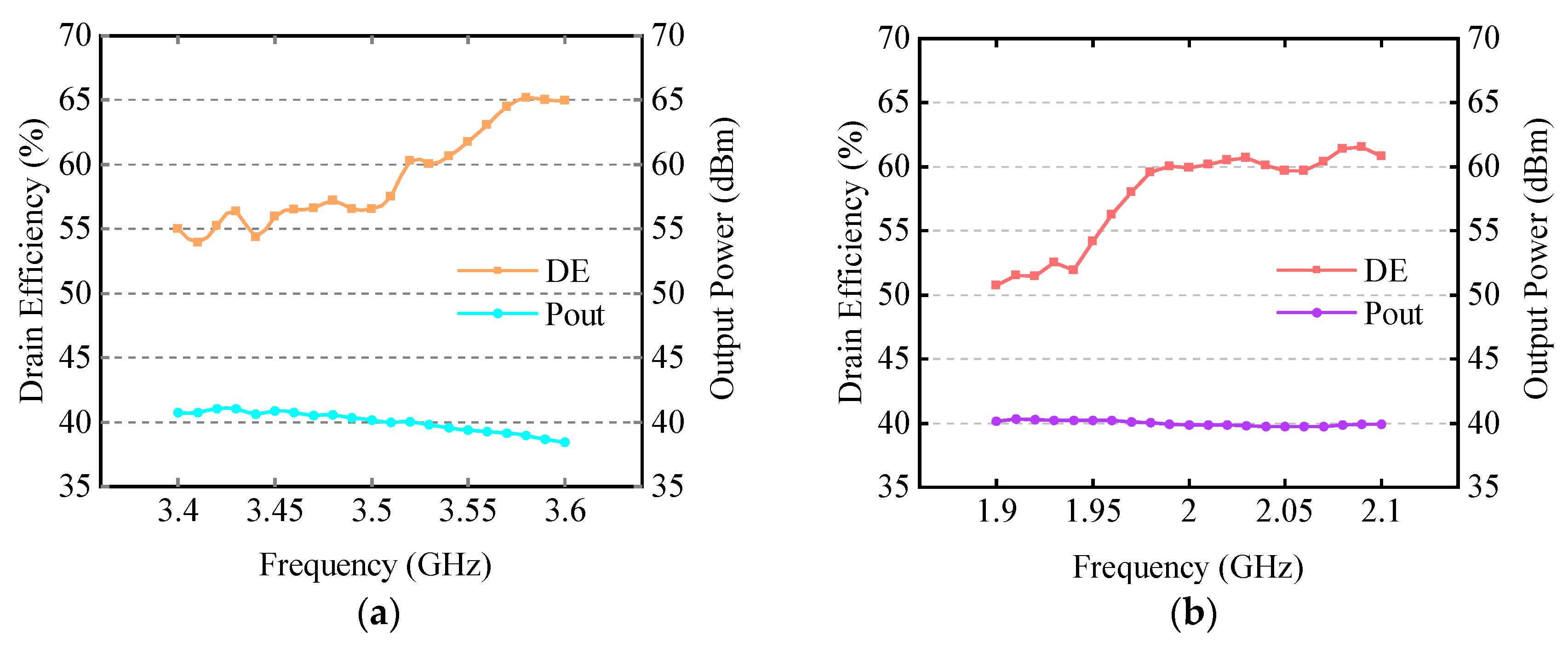
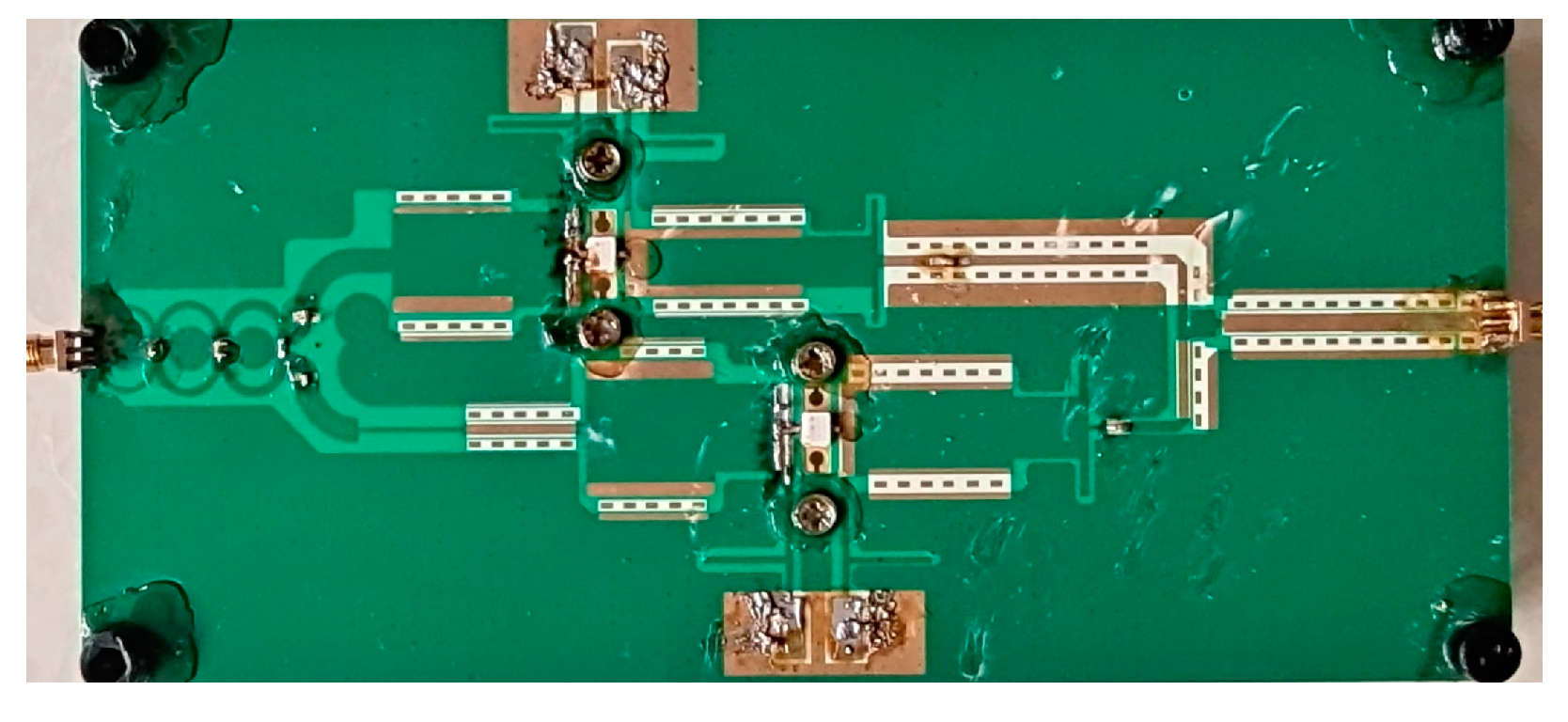
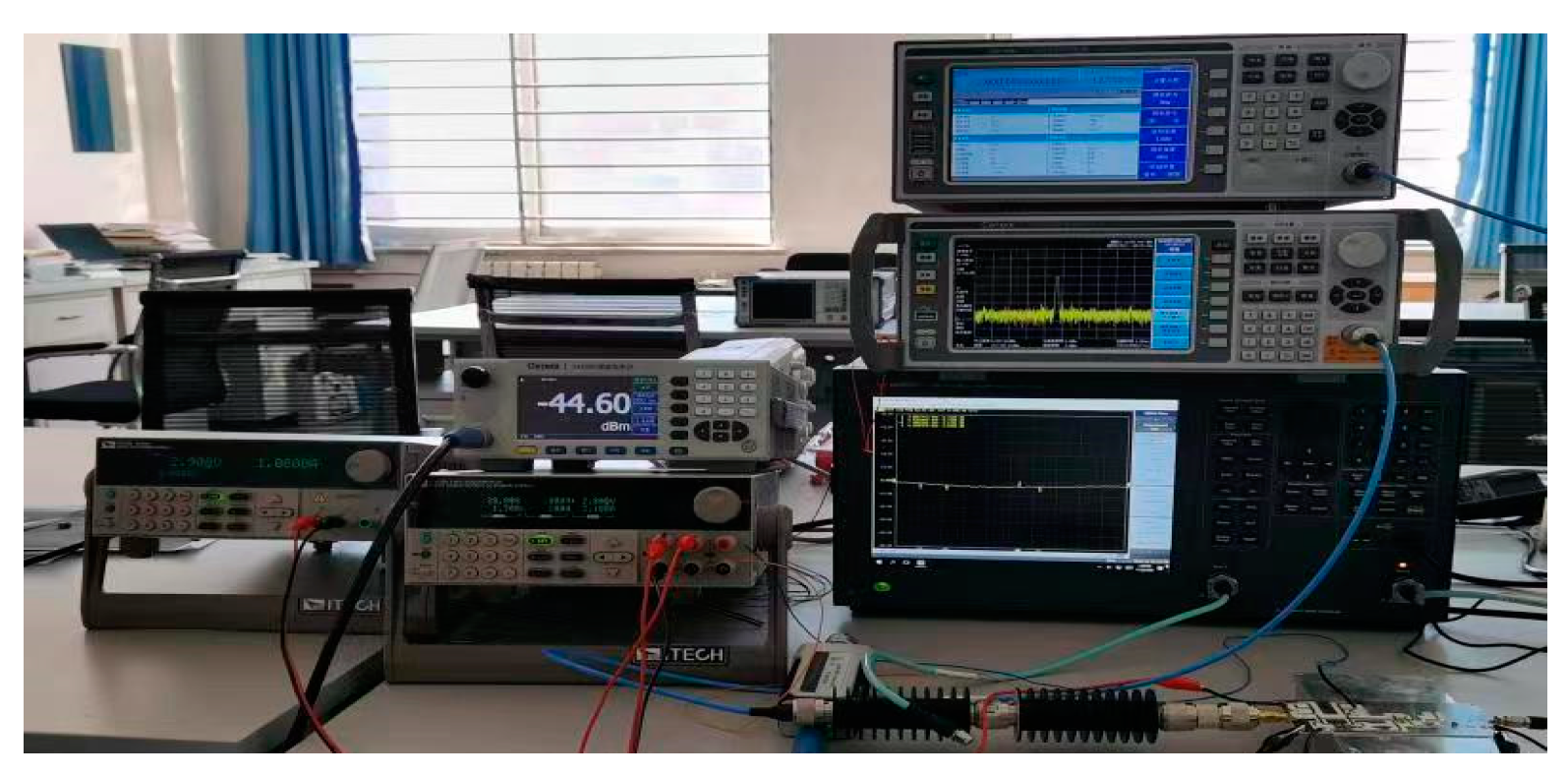
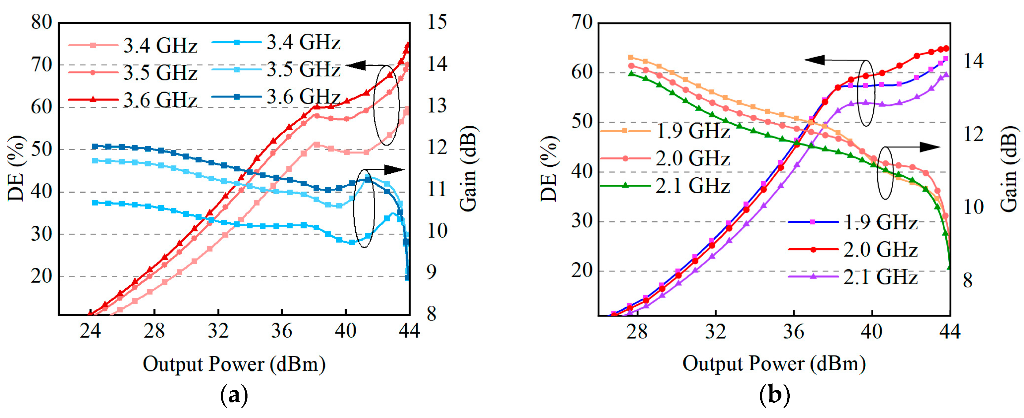
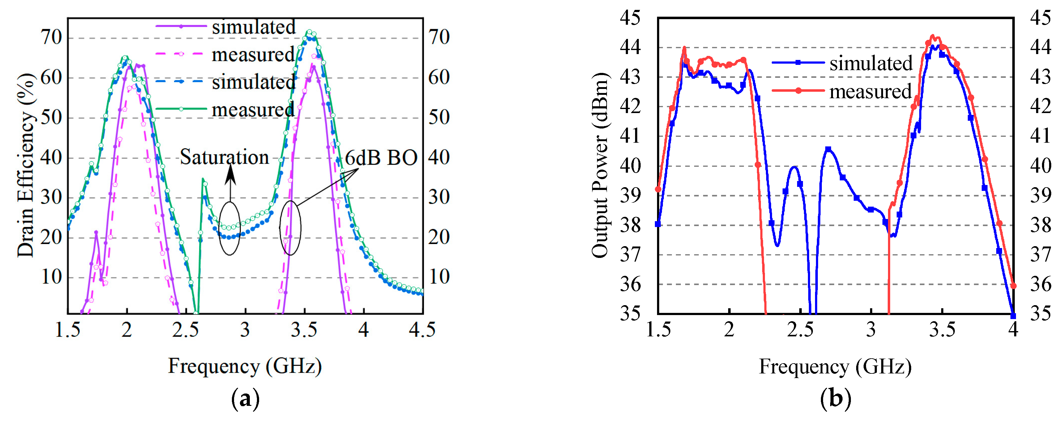
4. Results and Discussion

The basic sub-circuit of the designed concurrent dual-band Doherty power amplifier is realized, and all the circuit units are combined into the final circuit. The topology of the overall circuit consists of a broadband Wilkinson power divider, a carrier power amplifier, a peak power amplifier, and an impedance converter, as shown in Figure 12. To further validate the proposed design, physical fabrication and testing were carried out. The fabricated DPA is shown in Figure 13. Here, a 10 W Cree GaN transistor (CGH40010F) is used as the active device, and the substrate material used is Rogers4350B with a thickness of 0.762 mm, dielectric constant of 3.66, and tangent loss of 0.0037. The gate bias voltages for the carrier amplifier and the peak amplifier are −2.9 V and −5.4 V, respectively, and the drain bias voltages of both are 28 V.
The testing system consists of a vector network analyzer, a spectrum analysis instrument, a signal source, a driving stage power amplifier, an attenuator, a DC power supply, and a power amplifier to be tested. The photo of the measuring device is shown in Figure 14.
The overall circuit of the designed concurrent dual-band Doherty power amplifier is simulated and tested for drain efficiency and output power, as shown in Figure 15 and Figure 16. As shown in Figure 15, the simulation results show that the saturated drain efficiency of the concurrent dual-band Doherty power amplifier is 60–63%, the saturated output power reaches 43–44 dBm in the 1.9–2.1 GHz band, and the drain efficiency is 53–60% at the 6 dB back-off point. In the 3.4–3.6 GHz band, the concurrent dual-band power amplifier has a drain efficiency of 65–72% and saturated output power of 44–44.2 dBm, with drain efficiencies of 54–62% at the 6 dB back-off point.
The test results of the designed dual-band DPA in the 1.5–4.5 GHz band are shown in Figure 16. After testing, a bandwidth of about 200 MHz is available in both bands. The saturated output power reaches 43.4–43.7 dBm in the 2 GHz band, and drain efficiency reaches 57–65%; the 6 dB back-off efficiency is 49.7–57.4%. In the 3.5 GHz band, the saturated output power reaches 43.7–44.4 dBm, and drain efficiency reaches 65–71%; the 6 dB back-off efficiency is 53–65%. Near the 2.6 GHz band, the drain efficiency is almost zero, and the output power is below 40 dBm. In this design, the parallel dual-band Doherty power amplifier has an isolation band with trapping characteristics in the middle of the two bands and a transmission zero at about 2.6 GHz. The power amplifier is usually followed by a filter, which can be filtered using a dual-band bandpass filter to achieve better performance specifications.
The nonlinearity metrics of the power amplifier are also important, and here, the adjacent channel leakage ratio (ACPR) is used to measure the linearity of the designed concurrent dual-band Doherty power amplifier. Based on the WCMDA standard protocol of 3GPP, a 64 K modulated signal with a bandwidth of 5 MHz is used for testing. The results are shown in Figure 17, where the adjacent channel leakage ratios are tested for two frequency bands with frequency centers of 2.0 GHz and 3.5 GHz, respectively. As can be seen from the figure, after digital pre-distortion (DPD), the power values of the first and second adjacent channels are very small relative to the power of the main channel. This indicates that the transmitted signal has little interference with other signals and meets the requirements of international standards. Compared with other concurrent dual-band Doherty power amplifiers at home and abroad, as shown in Table 1, the concurrent dual-band Doherty power amplifier designed in this paper has certain advantages. The output power and efficiency have high specifications.

5. Conclusions

In this paper, a concurrent dual-band Doherty power amplifier operating at 2.0/3.5 is designed, and the designed power amplifier is simulated and physically tested. The test results show that the designed concurrent dual-band Doherty power amplifier achieves a saturated output power and drain efficiency of 44 dBm and 62%, respectively, and a 6 dB back-off efficiency of 53% in the 2 GHz band. The saturated output power and drain efficiency in the 3.5 GHz band reached 43.8 dBm and 68%, respectively, and the 6 dB back-off efficiency reached 58%. Finally, the power amplifier was also tested for the nonlinearity metric ACPR, which showed that the power in the adjacent channel was small relative to the power in the main channel. This design can provide an excellent solution for concurrent dual-band Doherty power amplifiers. In addition to this, the low-pass filter has a large bandwidth, and the use of real frequency techniques to enable precise matching of the saturation and fallback impedances of the dual-band may result in a larger bandwidth and better fallback efficiency.

Author Contributions

Conceptualization, G.L. and W.X.; methodology, G.L. and M.G.; software, W.X.; validation, G.L., J.N. and W.X.; formal analysis, W.X. and M.G.; investigation, G.L. and M.G.; resources, W.X.; data curation, G.L.; writing—original draft preparation, W.X.; writing—review and editing, G.L.; visualization, J.N. and W.X.; supervision, G.L., J.N. and M.G.; project administration, G.L. and J.N.; funding acquisition, G.L. and J.N.All authors have read and agreed to the published version of the manuscript.

Funding

This work was funded by the 1. Future-oriented Research on Wireless Reconfigurable Intelligent RADIO Module and Neural Network Modeling (61971210); 2. National Foundation: Power Amplifier Design Modeling and Predistortion Research for Cognitive Radio Systems under ComPressed Sensing Framework (61701211); and 3. Applied Basic Research Project of Liaoning Province(2022JH2/101300275).

Data Availability Statement

The data that support the findings of this study are available from the corresponding author, Wenyuan Xu, upon reasonable request.

Conflicts of Interest

The authors declare no conflict of interest.

References

  1. Liu, Y.; Li, C.; Xia, X.; Quan, X.; Liu, D.; Xu, Q.; Pan, W.; Tang, Y. Multiband User Equipment Prototype Hardware Design for 5G Communications in Sub-6-GHz Band. IEEE Trans. Microw. Theory Tech. 2019, 67, 2916–2927. [Google Scholar] [CrossRef]
  2. Lim, J.; Kang, W.; Ku, H. Compensation of path imbalance in LINC transmitters using EVM and ACPR look up tables. In Proceedings of the 2010 Asia-Pacific Microwave Conference, Yokohama, Japan, 7–10 December 2010; pp. 1296–1299. [Google Scholar]
  3. Su, Z.; Yu, C.; Tang, B. A Concurrent Dual-band Doherty Power Amplifier with Performance Enhancement Using a Novel Impendence Invert Network. In Proceedings of the 2019 IEEE MTT-S International Wireless Symposium (IWS), Guangzhou, China, 19–22 May 2019; pp. 1–3. [Google Scholar]
  4. Li, X.; Chen, W.; Zhang, Z.; Feng, Z.; Tang, X.; Mouthaan, K. A concurrent dual-band doherty power amplifier. In Proceedings of the 2010 Asia-Pacific Microwave Conference, Yokohama, Japan, 7–10 December 2010; pp. 654–657. [Google Scholar]
  5. Yang, F.; Yu, H.; Li, J.; Guo, C.; Yan, S.; Chen, X.; Zhang, A.; Jin, Z. A Class-F Based Power Amplifier with Optimized Efficiency in Triple-Band. Electronics 2022, 11, 310. [Google Scholar] [CrossRef]
  6. Abdulkhaleq, A.M.; Yahya, M.A.; McEwan, N.; Rayit, A.; Abd-Alhameed, R.A.; Ojaroudi Parchin, N.; Al-Yasir, Y.I.A.; Noras, J. Recent Developments of Dual-Band Doherty Power Amplifiers for Upcoming Mobile Communications Systems. Electronics 2019, 8, 638. [Google Scholar] [CrossRef]
  7. Rawat, K.; Ghannouchi, F.M. Design Methodology for Dual-Band Doherty Power Amplifier with Performance Enhancement Using Dual-Band Offset Lines. IEEE Trans. Ind. Electron. 2012, 59, 4831–4842. [Google Scholar] [CrossRef]
  8. Saad, P.; Colantonio, P.; Piazzon, L.; Giannini, F.; Andersson, K.; Fager, C. Design of a Concurrent Dual-Band 1.8–2.4-GHz GaN-HEMT Doherty Power Amplifier. IEEE Trans Microw Theory Tech. 2012, 60, 1840–1849. [Google Scholar] [CrossRef]
  9. Pang, J.; He, S.; Dai, Z.; Huang, C.; Peng, J.; You, F. Novel design of highly-efficient concurrent dual-band GaN Doherty power amplifier using direct-matching impedance transformers. In Proceedings of the 2016 IEEE MTT-S International Microwave Symposium (IMS), San Francisco, CA, USA, 22–27 May 2016; pp. 1–4. [Google Scholar]
  10. Yildiz, S.; Aksen, A.; Yarman, S.B. Dual band matching network design via real frequency technique by mapping from a band pass prototype. In Proceedings of the 2016 16th Mediterranean Microwave Symposium, Abu Dhabi, United Arab Emirates, 14–16 November 2016; pp. 1–4. [Google Scholar]
  11. Liu, M.; Golestaneh, H.; Boumaiza, S. A concurrent 2.15/3.4 GHz dual-band Doherty power amplifier with extended fractional bandwidth. In Proceedings of the 2016 IEEE MTT-S International Microwave Symposium, San Francisco, CA, USA, 22–27 May 2016; pp. 1–3. [Google Scholar]
  12. Cidronali, A.; Maddio, S.; Giovannelli, N.; Collodi, G. Frequency analysis and multiline implementation of compensated impedance inverter for wideband Doherty high-power amplifier design. IEEE Trans. Microw. Theory Tech. 2016, 64, 1359–1372. [Google Scholar] [CrossRef]
  13. Pang, J.; Dai, Z.; Li, Y.; Li, M.; Zhu, A. Multiband dual-mode Doherty power amplifier employing phase periodic matching network and reciprocal gate bias for 5G applications. IEEE Trans. Microw. Theory Tech. 2020, 68, 2382–2397. [Google Scholar] [CrossRef]
  14. Li, M.; Pang, J.; Li, Y.; Zhu, A. Ultra-wideband dual-mode Doherty power amplifier using reciprocal gate bias for 5G applications. IEEE Trans. Microw. Theory Tech. 2019, 67, 4246–4259. [Google Scholar] [CrossRef]
  15. Lee, Y.-S.; Lee, M.-W.; Kam, S.-H.; Jeong, Y.-H. A New Wideband Distributed Doherty Amplifier for WCDMA Repeater Applications. IEEE Microw. Wirel. Compon. Lett. 2009, 19, 668–670. [Google Scholar]
  16. Rubio, J.M.; Fang, J.; Camarchia, V.; Quaglia, R.; Pirola, M.; Ghione, G. 3–3.6-GHz Wideband GaN Doherty Power Amplifier Exploiting Output Compensation Stages. IEEE Trans. Microw. Theory Tech. 2012, 60, 2543–2548. [Google Scholar] [CrossRef]
  17. Kim, I.; Cha, J.; Hong, S.; Kim, J.; Woo, Y.Y.; Park, C.S.; Kim, B. Highly linear three-way Doherty amplifier with uneven power drive for repeater system. IEEE Microw. Wirel. Compon. Lett. 2006, 16, 176–178. [Google Scholar] [CrossRef]
  18. Kim, J.; Fehri, B.; Boumaiza, S.; Wood, J. Power efficiency and linearity enhancement using optimized asymmetrical Doherty power amplifiers. IEEE Trans. Microw. Theory Tech. 2011, 59, 425–434. [Google Scholar] [CrossRef]
  19. Pang, J.; He, S.; Dai, Z.; Huang, C.; Peng, J.; You, F. Design of a post-matching asymmetric Doherty power amplifier for broadband applications. IEEE Microw. Wirel. Compon. Lett. 2016, 26, 52–54. [Google Scholar] [CrossRef]
  20. Luo, Y.; Xuan, D.; Wang, Z.; Gao, W.; Yang, W.; Yuan, S. A concurrent 2.6/3.5GHz dual-band Doherty power amplifier with matching network based on composite right/left-handed unit cell. IEICE Electron. Express 2022, 19, 20210470. [Google Scholar] [CrossRef]
  21. Chen, H.; Xu, J.-X.; Chen, W.; Zhang, X.Y. High-Efficiency Dual-Band Filtering Doherty Power Amplifier Based on Multi-Function Circuit. IEEE Trans. Microw. Theory Tech. 2022, 70, 2697–2709. [Google Scholar] [CrossRef]
  22. Xuan, A.N.; Negra, R. Design of concurrent multiband biasing networks for multiband RF power amplifiers. In Proceedings of the 2012 42nd European Microwave Conference, Amsterdam, The Netherlands, 29 October–1 November 2012; pp. 1–4. [Google Scholar]
  23. Nasri, A.; Estebsari, M.; Toofan, S.; Piacibello, A.; Pirola, M.; Camarchia, V.; Ramella, C. Design of a Wideband Doherty Power Amplifier with High Efficiency for 5G Application. Electronics 2021, 10, 873. [Google Scholar] [CrossRef]
Figure 1. Overall structure of Doherty power amplifier.
Electronics 12 04092 g001
Figure 2. Low-pass filter circuit.
Electronics 12 04092 g002
Figure 3. Fourth-order impedance low-pass filter.
Electronics 12 04092 g003
Figure 4. Overall circuit of carrier power amplifier.
Electronics 12 04092 g004
Figure 5. Simulation results of saturated output power and drain efficiency of carrier power amplifier (a) at 3.4–3.6 GHz and (b) at 1.9–2.1 GHz.
Electronics 12 04092 g005
Figure 6. The input impedance of peak power amplifier output terminal (a) at 3.4–3.6 GHz and (b) at 1.9–2.1 GHz.
Electronics 12 04092 g006
Figure 7. Voltage phase diagram of carrier power amplifier and peak power amplifier (a) at 3.4−3.6 GHz and (b) at 1.9−2.1 GHz.
Electronics 12 04092 g007
Figure 8. Simulation results of peak power amplifier saturation output power and drain efficiency (a) at 3.4–3.6 GHz and (b) at 1.9–2.1 GHz.
Electronics 12 04092 g008
Figure 9. Schematic diagram of the three-stage λ/4 impedance converter.
Electronics 12 04092 g009
Figure 10. Schematic diagram of third-order Wilkinson power divider.
Electronics 12 04092 g010
Figure 11. Simulation results for S-parameters in the 1−4 GHz band of the power divider.
Electronics 12 04092 g011
Figure 12. Overall circuit diagram of Doherty and fabricated DPA.
Electronics 12 04092 g012
Figure 13. Fabricated dual-band DPA.
Electronics 12 04092 g013
Figure 14. Photograph of the measurement setup.
Electronics 12 04092 g014
Figure 15. Simulation of drain efficiency and gain (a) at 3.4–3.6 GHz and (b) at 1.9–2.1 GHz.
Electronics 12 04092 g015
Figure 16. Measured drain efficiency and output power at 1.5–4.5 GHz: (a) drain efficiency; (b) output power.
Electronics 12 04092 g016
Figure 17. Adjacent channel power leakage ratio of (a) primary channel power with a frequency center of 2.0 GHz and of (b) primary channel power with a frequency center of 3.5 GHz.
Electronics 12 04092 g017
Table 1. Performance comparison between this paper and other similar literature studies.
Ref.Frequency/GHzDE@Sat/DE@OBO/%Output Power@Sat/@OBO/dBm
[3]1.42/2.469.8/61 and 65.8/52.843.5/37.5 and 43.6/37.6
[7]1.8/2.464/60 and 54/4443/37 and 43/37
[8]0.85/2.3347.5/45 and 41/3544/38 and 42.5/36.5
[10]1.96/3.559.5/50.8 and 49.6/42.939.2/33.1 and 29.1/24.8
[11]1.42/2.2469/61 and 65.8/52.843.5/37.5 and 43.6/37.6
[20]2.6/3.555.8/49.6 and 55.2/49.343.3/38.5 and 43.6/38.5
[21]2.14/2.664.4/50 and 69/5743.25/37.25 and 43.3/37.3
This work2.0/3.566/55 and 71/6244.2/38.2 and 43.8/37.8
Disclaimer/Publisher’s Note: The statements, opinions and data contained in all publications are solely those of the individual author(s) and contributor(s) and not of MDPI and/or the editor(s). MDPI and/or the editor(s) disclaim responsibility for any injury to people or property resulting from any ideas, methods, instructions or products referred to in the content.

