
A Simplified Design Method for Quasi-Resonant Inverter Used in Induction Hob


1
Department of Electrical and Electronics Engineering, Istanbul Esenyurt University, 34510 Istanbul, Turkey
2
Department of Research and Development, Mamur Technology Systems Inc., 34590 Istanbul, Turkey
Electronics 2023, 12(19), 4145; https://doi.org/10.3390/electronics12194145
Submission received: 26 August 2023
/
Revised: 20 September 2023
/
Accepted: 21 September 2023
/
Published: 5 October 2023
Abstract
:Induction heating (IH) technology is widely recognized and utilized in residential applications due to its high efficiency and safe operating characteristics. Resonant inverter circuits are widely used in IH systems because of their high efficiency and ability to perform soft switching. Among the various resonant inverters used in IH systems, the single-switch quasi-resonant (SSQR) inverter topology is typically preferred for low-cost and low-output-power applications. Despite its cost advantage, the SSQR topology has a relatively narrow soft-switching range, which can be unstable depending on the electrical parameters of the load and the resonant converter circuit. Accurately determining the capacitance value of the resonant capacitor and the inductance value of the induction coil, which are the key circuit elements of the SSQR induction cooker, is crucial for designing a reliable, efficient, and durable cooking system. In other words, there exists a critical relationship between the resonant converter circuit parameters, load characteristics, and safe operating conditions. Additionally, when considering closed-loop control methods used for power control and safety, selecting appropriate resonant circuit elements becomes vital in ensuring both reliable and efficient operation. This paper focuses on a novel and simplified design method for the SSQR inverter utilized in household appliances. The proposed method and its advantages in terms of the safe operating area of the switch are theoretically investigated and verified through simulations and prototype circuits.
1. Introduction
Induction heating systems have gained significant popularity in industrial, domestic, and medical applications over the past few decades due to their notable features including user safety, efficient and rapid heating, and easy maintenance [1,2,3,4]. The advancements in power electronics as well as electronics have contributed to the progress of induction technology [5,6,7,8]. In domestic induction cooking appliances, one or more induction coils are positioned beneath a vitro ceramic glass surface to heat up pans placed on top of it [9,10,11]. The induction coil is supplied with an alternating current, generating a magnetic field at the same frequency as the coil current in order to heat the pan. This heating process occurs through the induction surface by inducing eddy currents in the pan [2,12]. The main components of induction heating systems consist of a rectifier unit for AC-DC conversion and resonant inverter units [13,14]. Figure 1 illustrates a general power-transfer loop for domestic appliances.
Power converters, which are a crucial component of induction heating systems, employ either single-stage or double-stage structures [15]. Double-stage systems involve both AC to DC and DC to AC conversions within IH systems [13,14]. In contrast, single-stage AC to AC systems lack a rectifier stage. These systems can be categorized into two groups: those that directly convert the input AC voltage and those that boost it.
Furthermore, induction heating systems are composed of either single or multiple loads/coils. In the past years, single-coil systems have been extensively utilized in both industrial and domestic induction applications. Recent advancements in multiple output induction heaters suggest enhancing performance through adjustable cooking surfaces [16,17,18]. The selection of different coil models depends on factors such as design requirements, cost, output power, and hob geometry. Various approaches are employed to configure cooking surfaces based on the pan size and coil design [16,19]. While pans made of ferromagnetic material are commonly used as loads, recent studies have also explored heating pans made of all-metal materials [20,21,22,23,24].
Different resonant inverter topologies have been proposed based on the trade-off between cost and performance, which needs to be evaluated for each specific application. The most common inverter topologies in induction heating (IH) systems are half-bridge series resonant (HBSR) [25,26,27,28] and single-switch quasi-resonant (SSQR) [29,30,31] inverters. The SSQR inverter topology provides a reliable solution for low-power and low-cost IH applications. However, the main drawback of the quasi-resonant inverter circuit is its inability to control the power transferred to the load in a frequency-controlled manner, as in HBSR inverter circuits. This limitation stems from the fact that the working modes of the SSQR inverter switch between and circuits [11,32]. Consequently, closed-loop control algorithms are employed to determine the turn-on and turn-off times of the semiconductor switch.
In IH systems utilizing SSQR inverters, a significant correlation exists among the resonant converter circuit, load parameters, current and voltage limits of the semiconductor switch, turn-on and turn-off times of the semiconductor switch, and closed-loop power control methodologies. Furthermore, when assessed in conjunction with the closed-loop control techniques employed for power regulation and safety purposes, the selection of resonant circuit elements assumes critical importance in guaranteeing a reliable and efficient operation.
Coil-equivalent inductance and resistance values, which form the electrical model of the system comprising the coil and the pan, are challenging to determine during the modeling of resonant circuit elements. Additionally, these values are subject to variations based on factors such as the operating frequency of the resonant circuit, ambient temperature, and air gap between the pan and the coil. As a result, there exists a wide range of academic research focusing on pan and load recognition [11,29,33,34,35,36]. However, the design of the coil itself necessitates a comprehensive academic investigation. Numerous studies have been conducted on coil design, particularly in the context of magnetic fields [37,38,39].
The wide range of electrical loads associated with pans used in domestic induction hob applications with SSQR inverters allows for customization of the electrical circuit parameters based on user preferences. Furthermore, the heat generated in the pan affects the values of circuit variables, such as resistance and inductance, and potential variations due to the electrical network necessitate certain assumptions to be made in the design of the heating system with the SSQR inverter.
In [40,41], a Class E inverter design utilizing one inductor and one capacitor is presented. During the initial stages of the design, semiconductor losses are disregarded, and it is assumed that the pan resistance remains constant. Additionally, the coil design precedes the circuit design, and the equivalent inductance () and equivalent resistance () values are determined based on the operating frequency (). Similarly, in [42], prior to the implementation of the related design, the input voltage (), work coil parameters (), water mass (), and required boiling time () must be defined. In [43], the design process requires the specification of inverter output power (P), DC input voltage (), resonant frequency (), as well as various other load and coil parameters. In [44], the inductance value is calculated based on the number of turns N, wire diameter W, and space S between consecutive turns. In [45], the finite-element method is employed, utilizing the coil’s geometry. It is noted that the inductance value varies due to the physical interaction between the coil and the ferromagnetic pan; however, there is no provided data regarding the specific inductance value for the pan.
As a result, the design of an induction heating hob generally encompasses various interconnected disciplines, including magnetic design, electronic circuit design, control theory, cooling system design, user preferences, and the like. Each designer begins the design process by establishing their own set of design criteria and methods. However, when circuit design begins with coil design and magnetic analyses, rather than determining the values of fundamental circuit variables, the subject can surpass its intended scope, and the design can become overly complex. The studies briefly mentioned above require that critical information such as coil geometry, coil design and coil inductance value must be defined before starting the circuit design, by making some assumptions. However, while designing the SSQR inverter system, it is very important to determine the coil inductance value, as in other converter designs. In other words, the purpose of the design is to determine the coil inductance value to be used in the SSQR inverter. Defining a certain value for coil inductance before starting the design will complicate the circuit design process and prolong the process of obtaining output values such as current, voltage, and power at desired values.
Also, in practical circuit design applications, using the inductance value as an input parameter may not be as practical as described in the references provided. From this point of view, the proposed method provides a feasible design approach for initial conditions where the critical circuit parameters of the resonant circuit, namely coil inductance ), equivalent circuit resistance and resonant circuit capacitor value ( are not known, by utilizing the energy desired to be transferred to the coil inductor.
Input parameters, such as the mains input voltage , the output power (P) to be transferred to the pan, and the switching times of the semiconductor are determined before the design phase. Then all circuit parameters, including , , and , can be determined using the proposed calculation method. In short, if the designer knows the desired power output, grid voltage, and operating frequency to be applied to the cooker before starting the design, they will easily have a circuit design for the SSQR inverter. Through the proposed method, an innovative design tool will be obtained which is not found in the reference studies in the literature and remains unquestioned in practical application. In this way, it is aimed to create a reference method especially for practitioners who are new to SSQR design.
The rest of the manuscript is structured as follows: In Section 2, the circuit description of the SSQR inverter converter is explained. In Section 3, the detailed proposed design method of SSQR inverter is summarized. Section 4 shows the calculation, simulation, and experimental results, respectively. The conclusion of this study is outlined in Section 5.
2. Circuit Description
The circuit diagram and schematic of the single-switch quasi-resonant inverter, along with its primary operational waveforms, are presented in Figure 2 and Figure 3, respectively. The circuit schematic comprises a semiconductor switch denoted as , a freewheeling diode labeled , an equivalent resistance represented by , an equivalent inductance designated as , and a resonance capacitor denoted as . Upon the activation of the T switch, the circuit behaves analogously to a series circuit. During this phase, the coil accumulates energy through the resistance over a duration labeled as . Throughout the turn-on time, the coil accumulates energy provided by the primary voltage source .
When the switch is closed, the circuit starts to work as a series circuit. In this configuration, resonance is established between the coil and the capacitor, facilitating energy exchange. The resonance capacitor, , charges to the peak voltage, , and eventually discharges to zero. A short time after the capacitor has completely discharged, the switch is promptly reactivated, in accordance with references [1,46,47].
2.1. Circuit Operating Modes—Waveform Equations
The operational modes of the single-switch resonant inverter, depicted in Figure 4, are examined across four primary operational stages. The conduction period of the semiconductor, denoted as , is mathematically modeled as a series circuit incorporating components and . Simultaneously, the time interval , characterized by resonance interactions between and , is subjected to analysis as a series RLC circuit. Lastly, the conduction duration of the freewheeling diode, , is depicted through a series circuit model. Owing to the behavior of the single-switch resonant inverter as a series circuit during states 2 and 3 among the four operational states and as a series circuit during states 1 and 4, the associated circuit is evaluated in the time domain as opposed to the frequency domain.
Throughout the analysis, particular attention is directed towards steady-state analysis, with a focus on the initial operational stage. Potential phenomena like resonance capacitor discharge current and analogous transient states are deliberately disregarded for the sake of analytical simplicity.
Stage I : This interval commences with the initiation of the semiconductor under zero voltage conditions (ZVT) and persists until the switch deactivates. Regarding the operation of the circuit, the subsequent equations can be formulated as illustrated in Equations (1)–(3) [48].
Stage II–III : This interval initiates with the deactivation of the semiconductor, and the resonance phenomenon between and is scrutinized through analysis as a series circuit. Furthermore, the subsequent equations can be established to characterize the current , as depicted in Equations (4)–(7) [48].
diLEQ (t0)/dt ⟹
Furthermore, the mentioned equations, along with the circuit Equations (8)–(11), can be employed to compute the switch collector–emitter voltage as illustrated in Figure 3.
Stage IV : This interval initiates with the activation of the diode, which is connected anti-parallel to the power switch. As depicted in Figure 3, the dissipation of current or energy through the source is managed by a power diode. Regarding the operation of the circuit, the ensuing equations can be formulated as demonstrated in Equations (12)–(15). The duration of diode current conduction, , and the peak diode current are denoted as .
2.2. Safe Operating Area for Quasi-Resonant Inverter
From the provided first- and second-order circuit equations, it is evident that the precise determination of values hold paramount importance for ensuring the secure operational conditions of quasi-resonant induction heating applications. The chief threats to safe functionality within power electronic circuits encompass both elevated voltage and current surpassing the maximum operational thresholds of the employed semiconductors. Although all constituents of electronic circuits can be influenced by overcurrent and overvoltage stress, semiconductor switches stand out as the most vulnerable elements in inverter applications. Even if excess heat generated by excessive current can be mitigated through enforced cooling methodologies, semiconductors subjected to voltages surpassing their breakdown thresholds can promptly render them non-operational. By employing the PSpice simulation program, variations in the collector–emitter voltage () of the semiconductor switch are assessed across diverse resonant circuit parameter configurations, as visually depicted in Figure 5.
Similarly, discharge currents of the capacitor, frequently observed within quasi-resonant inverter circuits, pose a threat to the reliable operational conditions of both semiconductors and power electronics circuits. These instantaneous currents, also referred to as light-load currents, can exceed the nominal maximum current of the semiconductor (or coil current ) by three to four times, resulting in issues such as overheating, stress, and similar challenges. Just like the voltage example, the semiconductor switch current is derived using the PSpice simulation program, contingent upon resonant circuit parameters, as depicted in Figure 6.
Nonetheless, closed-loop power control techniques and the assessment of input parameters play a pivotal role in ensuring dependable operational conditions. When scrutinizing the quasi-resonant inverter, it becomes evident that its operating modes oscillate between and circuits. Consequently, the implementation of closed-loop control methodologies to ascertain the turn-on and turn-off timings of semiconductor switches emerges as indispensable. Depending on the material characteristics, AC supply conditions, and parameters of inverter circuit elements, miscalculations in semiconductor switch turn-on or turn-off times exceeding can swiftly escalate switching losses. This outcome can render the switch inoperative due to either overheating or overvoltage occurrences.
In the next section, a new simplified design method for an SSQR inverter used in household appliances is examined.
3. Proposed Design Method for Quasi-Resonant Inverter
Before starting the inverter design, the circuit variables that we use as input variables and known before the design should be defined correctly and the related design should be guided by using known circuit variables. In this study, the DC source voltage ) obtained as a result of rectifying the AC mains voltage, the average input power drawn from the main source, and the semiconductor switch turn-on-time () and turn-off-time variables are used as the initial conditions. The method to be followed in the design can be summarized as follows:
- The DC source voltage ), the average input power , and the switch turn-on-time () and turn-off-time ( variables are defined.
- The maximum value of the coil current is calculated with the help of the relevant circuit equations.
- By detecting the first harmonic component of the voltage applied to the resonant circuit, the load resistance is calculated.
- After calculating the load resistance, the equivalent inductance value, is calculated with the help of the circuit equations.
- The of the series circuit are determined with the help of calculated variables.
- The resonant capacitor value is calculated with the help of resonant frequency and inductance value .
- The design is verified by calculating the coil current and capacitor voltage boundary conditions.
3.1. Defining of the Time Intervals and , the Source Voltage , and the Input Power
In order not to operate at the audible frequency value, the operating frequency values of household induction hobs are not preferred below the threshold frequency value [49,50,51]. On the other hand, to increase the switching frequency will increase the switching losses of the semiconductors used [4,49,52].
For these reasons mentioned above, SSQR inverters used in induction cookers are operated in the range of . It should also be noted that SSQR inverter circuits cannot be operated directly with frequency control, as with half-bridge inverters. time is determined by controlling the resonance oscillation of the energy transferred to the load during the time. The predefined values for starting in this design study are and . The source voltage is obtained by rectifying the mains voltage, as shown in Figure 7.
The purpose of the capacitor used at the output of the rectifier is to provide the instantaneous currents demanded by the inverter circuit and act as a filter. Therefore, the voltage obtained follows the form of the main. In order to make the calculations easy and understandable, first of all, voltage will be accepted as a voltage source, and then the calculation values will be updated for the case where voltage follows the mains voltage form. The case where the source voltage is the voltage source is shown in Figure 7, and the case where follows the mains voltage form is shown in Figure 8. Finally, the predefined average source power for this design study is defined as .
3.2. Calculation of the Maximum Coil Current
In the case of quasi resonant inverter circuit operating in operating mode, the coil current equals the semiconductor switch current (). When the operating states of the quasi-resonant inverter circuit are examined, finding the maximum value of the switch current means finding the approximate maximum value of the coil current .
When the source voltage, is considered constant as the voltage source, the power–time graph becomes the multiplier of the current–time graph. The switch current and input power graphs as a function of time are shown in Figure 9 and Figure 10, respectively. The variation in circuit switch current with time depends on the values of and and is defined by Equation (18) in case .
From Equation (18), it is clear that the graphs of and cannot be linear and will behave variably depending on the circuit values. However, since the resistance values created by the pans used in induction heated cookers in the primary circuits are in the range of , accepting these graphs as linear will be very useful for finding the current. For the case where the average power transferred to the circuit is defined as and the instantaneous maximum power is defined as , the following equation is obtained with the help of Figure 10.
As a result of Equation (19), the value can be easily calculated (20).
On the other hand, for the case where the source voltage follows the mains voltage form, let us define the switch current and power variables as shown below:
→
→
→
→
Equation (21) is written for the case where the average power drawn from the source during the interval is accepted as , and the average power drawn from the source only at the time of π/2 is accepted as .
And then Equation (21) is simplified, and Equation (22) is obtained.
When Equations (19) and (20) are rearranged,
As can be easily seen from Equations (23) and (24), the switch current and the instantaneous maximum power value to be obtained for the case where the source voltage follows the mains voltage will increase by compared to the case where the source voltage is . This is because the same value is desired to be drawn from the source, regardless of the source voltage form.
3.3. Calculation of Value by Determining the First Harmonic Component of the DC Voltage
Assuming that the resonant circuit current is sinusoidal, the first harmonic component of the voltage applied to the resonant circuit is obtained. In this way, the value of resistance, is reached by using the maximum value of the resonant circuit current. According to the Fourier theorem, any practical periodic function with an angular frequency of can be expressed as an infinite sum of sine or cosine functions that are integer multiples of [48]. Thus, can be expressed as
The value is the mean value of the function and is indicated by the below equation.
The variation in voltage applied to the quasi-resonant circuit as a function of time is shown in Figure 11. The value of is found with the help of Equation (26) so that the value is the period of the function.
And then, and values of the related voltage waveform will be found.
In (30) is the amplitude value of the first harmonic component of the function. And so, the next steps are to find the amplitude, in other words, the peak value of the first harmonic component of the voltage applied to the quasi-resonant circuit, and to reach the value by proportioning this value to the maximum value of the coil current .
3.4. Calculation of the Equivalent Inductance Value
In order to calculate the inductance value, three different methods are used, and the results are compared with each other and verified. The first of these is to use the current equation of the series RL circuit, the second is to use the voltage at the inductor ends, and the third is to calculate the inductance value by using the energy accumulated in the inductor.
3.4.1. LEQ Calculation Using Series Circuit Switch Current Value
As mentioned earlier, the series circuit switch current as a function of time depends on the and values and is defined by Equation (32) for .
Since the source voltage ), equivalent resistance (, maximum value of coil current ) and time information are now known, the value can be found by using Equation (33).
3.4.2. LEQ Calculation Using Inductor Voltage Value
Equation (34) is obtained by using Kirchhoff’s voltage law in the series circuit.
And also, the voltage at the inductor ends is presented by the below Equation (35).
We will also make the linearity assumption that we used when finding the current in the series circuit. The inductance value for this range where the semiconductor switch and coil currents are equal to each other indicated by the below equation.
Although the voltage is constant, the voltage is expressed as (37) for the case where the current is considered linear.
When this expression is substituted in (36), Equation (38) is reached.
3.4.3. LEQ Calculation Using Inductor Energy Value
The energy accumulated in the inductor is expressed by the Equation (39) in terms of inductance and inductor current.
When the area under the graph shown in Figure 10 is integrated, the total energy transferred to the series circuit is found. Assuming the graph as linear (40) is found,
To find the total energy transferred to the inductor, the energy dissipated in the resistor is subtracted from the total energy transferred to the series circuit.
Equation (42) is obtained as a result of Equations (40) and (41).
After the energy accumulated in the inductor is reached, Equation (43) is used to arrive at the equivalent inductance.
And finally, we obtain Equation (44) with the help of Equations (39) and (43).
3.5. Determination the Series RLC Circuit Parameters
Since the time, which is the turn-off time of the semiconductor switch, is defined and known before the design, and the and values are calculated, the damping coefficient ), resonant frequency , and damped resonant frequent values of the series circuit can be calculated easily. First, the damped resonant frequency is calculated by using the relationship between the time and the resonant frequency of the series circuit.
And then, the damping coefficient of the series circuit is found by Equation (49).
Finally, the resonant frequency, , is calculated with the help of Equation (51).
3.6. Calculation of the Resonant Circuit Capacitor Value Inductance Value
After calculating the resonant frequency, , and the equivalent inductance, , values, the resonant circuit capacitance value, , is found by using Equation (52).
3.7. Calculation of Current and Voltage Boundary Conditions of Semiconductor Switch
Defining boundary conditions for the single-switch inverter design is very important. In working stage II and stage III (series circuit mode), the coil current, , and switch voltage, values reach their maximum values. Knowledge about these two parameters is very important and valuable for the designer not only for reliable working conditions but also to control system parameters, such as power. As it can be seen from Figure 3 that when the coil current reaches its maximum value, , the derivation of the current is zero (). As result of this, the maximum coil current, can be derived with the help of (54)–(56).
The single-switch induction cooker’s maximum power level is limited by the power switch maximum breakdown voltage level. When the switch voltage reaches its maximum value, , the current is zero (). As result of this, the maximum switch voltage, can be derived with the help of (57)–(59).
3.8. The Flowchart of the Proposed Design Method
The flowchart shown in Figure 12 is developed to understand the determining of the and more clearly. It determines the boundary conditions of the semiconductor switch with the help of the same flow chart. If the boundary conditions are not within the defined safe limit values of the semiconductor, the design is started from the beginning.
4. Verification of Proposed Analysis Method
In order to prove the accuracy of the proposed design method, first of all, critical circuit parameter values are calculated using predefined input parameters depending on the design requirements. By using the circuit parameters obtained as a result of the calculation, simulation studies are carried out and the boundary conditions required to ensure reliable operation of the inverter circuit are measured.
4.1. Calculation Results
As a result of the proposed method and calculation tools, a standard design example has been carried out, and the calculated results are listed in Table 1. Firstly, the initial values are defined, and then the critical circuit elements’ values are calculated. As previously mentioned, the average source power for this design study is defined as the . And also, the switch turn-on and turn-off times are defined as the and . The source voltage, is obtained by rectifying the mains voltage.
The critical circuit elements values are calculated as , , and . In addition to circuit parameters and , the current and voltage boundary conditions of the semiconductor switch are calculated to check design reliability. As can be seen from Table 1, depending on the input values defined for this study, the maximum value of the switch voltage, is calculated as , and the maximum value of the switch current, is calculated as .
4.2. Simulation Results
A simulation prototype circuit has been developed using the predefined and calculated circuit parameters from Table 1, and it is shown in Figure 13. The OrCAD PSpice (Version 17.2-2016) software program has been used for the simulation, with a particular emphasis on ensuring that the maximum coil current () and maximum switch voltage () values align with the values calculated in the previous section.
When the critical circuit element values obtained from measurement results were directly used in the designed circuit for simulation, some deviations were observed in the and values. The measured switch voltage was found to be instead of the expected , resulting in an error of approximately . Similarly, the maximum coil current, which should have been , was measured as , indicating an error of approximately .
Although the deviation values might be acceptable for many designers, the root cause of the discrepancy has been investigated to continue the simulation studies. It was hypothesized that the deviation arose from the proposed design method, which assumed a linear current–time graph by neglecting the resistance value in the RL operating mode of the SSQR inverter. Based on this assumption, a sweep analysis method has been employed in the relevant simulation program, scanning resistance values between and with a precision of . The resistance value that yielded the same current and voltage values as the calculated ones has been determined. Figure 14 illustrates the graph of the obtained current and voltage values from the scanning process. It has been observed that when a resistance value of was used instead of the calculated resistance value of , and the calculated values matched exactly with the simulation results. All the results obtained from the scanning process are presented numerically in Table 2.
To compare the results from the simulation circuit with the application circuit under the same conditions, the coil current () and switch voltage () graphs are separately presented over a 20 ms time interval in Figure 15 and Figure 16. The primary advantage of this representation is to provide a comprehensive and detailed understanding of how these variables change over time for those examining the study. By placing the simulation and application circuit results side by side, researchers can directly compare them and assess the accuracy or deviation between the simulated and actual circuit performance. This comparative analysis allows for a better understanding of the similarities and differences, enabling researchers to gain insights into potential factors that may affect the circuit’s behavior. Furthermore, by examining the variation in coil current and switch voltage over time, researchers can gain valuable insights into the dynamic behavior of the circuit. This information can be used to optimize the circuit’s performance, identify potential issues, such as transient spikes or oscillations, and make informed design decisions to ensure the circuit operates within desired parameters.
4.3. Experimental Results
Once the theoretical calculations and simulation studies developed for the calculation of critical circuit parameters are completed, the outputs of the proposed calculation method are tested using a practical application circuit. Before examining the results of the application circuit, it is beneficial to review the technical specifications of the induction coil and the heated pans used in the application circuit. This will facilitate the interpretation of deviations between the practical application results and the theoretical calculations and simulation circuit results.
As described in detail in the introduction of the study, a wide range of pan types are used in household induction cooktops. The electrical effects of these pans on the electronic circuitry are particularly critical due to their ability to change the equivalent resistance and equivalent inductance values. However, it is not feasible to test all possible pan models in practical applications. Therefore, in the experimental implementation of the proposed method, three different pan models with different electrical and magnetic characteristics, as shown in Figure 17, have been used. These pan models include cast iron, stainless steel, and specially designed alloy pans for induction heating.
On the other hand, Table 3 provides the physical and electrical characteristics of the induction coil used in the practical application circuit, as well as the measured equivalent inductance and resistance values when using three different types of pans. In practical application, although an exact match of the calculated resistance and inductance values obtained through the proposed calculation method is not achieved, the feasibility of the proposed method has been demonstrated.
In practical household usage, commonly encountered cookware materials such as cast iron, stainless steel, and silit silargan exhibit distinct ferromagnetic and electrical properties. When these cookware types are used on an induction cooktop, it results in different coil currents and switching voltages. The coil current, the switch voltage, and the output power values obtained when using three different pan models are presented in Table 4.
In addition, in Table 5, the output results obtained using the calculation, simulation, and application circuit for similar conditions are compared. Upon closer examination of Table 5, it is evident that the values obtained through the calculation method closely match the nearest capacitor value used.
However, the different electrical characteristics of the pans used in practical applications make it challenging to directly compare the calculation and application circuits. In practical implementation, a coil current of and a switch voltage of have been measured for a resistance of , while in the theoretical calculations and simulation circuit, these values were and , respectively. The deviation is approximately for current and for voltage. The main reason for this discrepancy is the change in the resistance and inductance values measured at the initial conditions when the pan is heated. As a result of these studies, considering the variety of pans used in practical applications, the proposed calculation method is proven to be reliable for initiating the design process.
To compare the results from the simulation circuit with the application circuit under the same conditions, the coil current () and switch voltage () graphs are separately presented over a 20 ms time interval in Figure 18 and Figure 19. When comparing these graphs with the results obtained from the simulation circuit in Figure 15 and Figure 16, it is evident that very similar results can be achieved. Also, the detailed waveforms of the coil current and switch voltage are shown in Figure 20. Finally, the experimental setup is shown in Figure 21.
5. Conclusions
In IH systems utilizing SSQR inverters, the selection of resonant circuit elements assumes critical importance in guaranteeing a reliable and efficient operation. This paper is focused on a new simplified design method for the SSQR inverter used in household appliances. Before starting the inverter design, the circuit variables that we use as input variables and known before the design should be defined correctly, and the related design should be guided by using known circuit variables. In this study, the DC source voltage () obtained as a result of rectifying the AC mains voltage, the average input power ) drawn from the main source, and the semiconductor switch turn-on time ( and turn-off time ( variables are used as the initial conditions. Then, all circuit parameters, including , and are determined using the proposed calculation method. In order to prove the accuracy of the proposed design method, first of all, critical circuit parameter values are calculated using predefined input parameters depending on the design requirements. By using the circuit parameters obtained as a result of the calculation, simulation studies are carried out, and the boundary conditions required to ensure reliable operation of the inverter circuit are measured.
After the completion of the theoretical background and simulation studies developed for use in critical circuit parameter calculation studies, the outputs of the relevant design method are run with the help of a practical application circuit. The results obtained from the experimental circuit are also compatible with the simulation results. The reliability of the proposed design and calculation method is proven by comparing the data obtained as a result of the simulations and experiments with the data obtained as a result of the calculations. In this way, we aimed to create a reference method especially for practitioners who are new to SSQR design.
Funding
This work was supported by the Scientific and Technological Research Council of Turkey and co-financed by the Mamur Technology Systems Research and Development Center under Project 3210188.
Data Availability Statement
No new data were created.
Conflicts of Interest
The author declares no conflict of interest.
References
- Komatsu, W.P.W. A simple and reliable class E inverter for induction heating applications. Int. J. Electron. 1998, 84, 157–165. [Google Scholar] [CrossRef]
- Omori, H.; Nakaoka, M. New single-ended resonant inverter circuit and system for induction-heating cooking apparatus. Int. J. Electron. 1989, 67, 277–296. [Google Scholar] [CrossRef]
- Tanaka, T. A new induction cooking range for heating any kind of metal vessels. IEEE Trans. Consum. Electron. 1989, 35, 635–641. [Google Scholar] [CrossRef]
- Lucía, O.; Maussion, P.; Dede, E.; Burdío, J.M. Induction heating technology and its applications: Past developments, current technology, and future challenges. IEEE Trans. Ind. Electron. 2014, 61, 2509–2520. [Google Scholar] [CrossRef]
- Lucia, O.; Navarro, D.; Guillen, P.; Sarnago, H.; Lucia, S. Deep Learning-Based Magnetic Coupling Detection for Advanced Induction Heating Appliances. IEEE Access 2019, 7, 181668–181677. [Google Scholar] [CrossRef]
- Has, U.; Wassilew, D. Temperature control for food in pots on cooking hobs. IEEE Trans. Ind. Electron. 1999, 46, 1030–1034. [Google Scholar] [CrossRef]
- Ekkaravarodome, C.; Charoenwiangnuea, P.; Jirasereeamornkul, K. The simple temperature control for induction cooker based on class-e resonant inverter. In Proceedings of the 2013 10th International Conference on Electrical Engineering/Electronics, Computer, Telecommunications and Information Technology, Krabi, Thailand, 15–17 May 2013; pp. 1–6. [Google Scholar]
- Kazimierczuk, M.K.; Wang, S. Frequency-domain analysis of series resonant converter for continuous conduction mode. IEEE Trans. Power Electron. 1992, 7, 270–279. [Google Scholar] [CrossRef]
- Lucia, O.; Sarnago, H.; Burdio, J.M. Soft-stop optimal trajectory control for improved operation of the series resonant multi-inverter. In Proceedings of the IECON 2014—40th Annual Conference of the IEEE Industrial Electronics Society, Dallas, TX, USA, 29 October 2014–1 November 2014; pp. 3283–3288. [Google Scholar] [CrossRef]
- Paesa, D.; Franco, C.; Llorente, S.; Lopez-Nicolas, G.; Sagues, C. Adaptive simmering control for domestic induction cookers. IEEE Trans. Ind. Appl. 2011, 47, 2257–2267. [Google Scholar] [CrossRef]
- Ozturk, M.; Zungor, F.; Emre, B.; Oz, B. Quasi Resonant Inverter Load Recognition Method. IEEE Access 2022, 10, 89376–89386. [Google Scholar] [CrossRef]
- Crisafulli, V.; Pastore, C.V. New control method to increase power regulation in a Ac/Ac quasi resonant converter for high efficiency induction cooker. In Proceedings of the 2012 3rd IEEE International Symposium on Power Electronics for Distributed Generation Systems, PEDG, Aalborg, Denmark, 25–28 June 2012; pp. 628–635. [Google Scholar]
- Sarnago, H.; Lucia, O.; Mediano, A.; Burdio, J.M. A Class-E Direct AC–AC Converter with Multicycle Modulation for Induction Heating Systems. IEEE Trans. Ind. Electron. 2014, 61, 2521–2530. [Google Scholar] [CrossRef]
- Sarnago, H.; Lucia, O.; Mediano, A.; Burdio, J.M. Direct AC–AC Resonant Boost Converter for Efficient Domestic Induction Heating Applications. IEEE Trans. Power Electron. 2014, 29, 1128–1139. [Google Scholar] [CrossRef]
- Vishnuram, P.; Ramachandiran, G. Capacitor-less induction heating system with self-resonant bifilar coil. Int. J. Circuit Theory Appl. 2020, 48, 1411–1425. [Google Scholar] [CrossRef]
- Park, H.P.; Kim, M.; Jung, J.H.; Kim, H.S. Load adaptive modulation method for all-metal induction heating application. In Proceedings of the 2018 IEEE Applied Power Electronics Conference and Exposition (APEC), San Antonio, TX, USA, 4–8 March 2018; pp. 3486–3490. [Google Scholar] [CrossRef]
- Sarnago, H.; Lucia, O.; Burdio, J.M. Multiple-output ZCS resonant inverter for multi-coil induction heating appliances. In Proceedings of the 2017 IEEE Applied Power Electronics Conference and Exposition (APEC), Tampa, FL, USA, 26–30 March 2017; pp. 2234–2238. [Google Scholar] [CrossRef]
- Lucia, O.; Carretero, C.; Palacios, D.; Valeau, D.; Burdío, J.M. Configurable snubber network for efficiency optimisation of resonant converters applied to multi-load induction heating. Electron. Lett. 2011, 47, 989–991. [Google Scholar] [CrossRef]
- Huang, M.S.; Liao, C.C.; Li, Z.F.; Shih, Z.R.; Hsueh, H.W. Quantitative Design and Implementation of an Induction Cooker for a Copper Pan. IEEE Access 2021, 9, 5105–5118. [Google Scholar] [CrossRef]
- Jeong, S.H.; Il Jin, J.; Park, H.P.; Jung, J.H. Enhanced load adaptive modulation of induction heating series resonant inverters to heat various-material vessels. J. Power Electron. 2022, 22, 1020–1032. [Google Scholar] [CrossRef]
- Han, W.; Chau, K.T.; Liu, W.; Tian, X.; Wang, H. A Dual-Resonant Topology-Reconfigurable Inverter for All-Metal Induction Heating. IEEE J. Emerg. Sel. Top. Power Electron. 2022, 10, 3818–3829. [Google Scholar] [CrossRef]
- Ramalingam, S.R.; Boopthi, C.S.; Ramasamy, S.; Ahsan, M.; Haider, J. Induction heating for variably sized ferrous and non-ferrous materials through load modulation. Energies 2021, 14, 8354. [Google Scholar] [CrossRef]
- Jin, J.; Kim, M.; Han, J.; Kang, K.; Jung, J.H. Input voltage selection method of half-bridge series resonant inverters for all-metal induction heating applications using high turn-numbered coils. J. Power Electron. 2020, 20, 1629–1637. [Google Scholar] [CrossRef]
- Jang, E.; Park, S.M.; Joo, D.; Ahn, H.M.; Lee, B.K. Analysis and Comparison of Topological Configurations for All-Metal Induction Cookers. J. Electr. Eng. Technol. 2019, 14, 2399–2408. [Google Scholar] [CrossRef]
- Sarnago, H.; Lucía, Ó.; Mediano, A.; Burdío, J.M. Analytical Model of the Half-Bridge Series Resonant Inverter for Improved Power Conversion Efficiency and Performance. IEEE Trans. Power Electron. 2015, 30, 4128–4143. [Google Scholar] [CrossRef]
- Hsieh, H.I.; Kuo, C.C.; Chang, W.T. Study of half-bridge series-resonant induction cooker powered by line rectified DC with less filtering. IET Power Electron. 2023, 16, 1929–1942. [Google Scholar] [CrossRef]
- Sarnago, H.; Guillén, P.; Burdío, J.M.; Lucia, O. Multiple-Output ZVS Resonant Inverter Architecture for Flexible Induction Heating Appliances. IEEE Access 2019, 7, 157046–157056. [Google Scholar] [CrossRef]
- Koertzen, H.W.; Van Wyk, J.D.; Ferreira, J.A. Design of the half-bridge, series resonant converter for induction cooking. In Proceedings of the IEEE Power Electronics Specialist Conference Records, Atlanta, GA, USA, 18–22 June 1995; Volume 2, pp. 729–735. [Google Scholar] [CrossRef]
- Altintas, N.; Ozturk, M.; Oktay, U. Performance evaluation of pan position methods in domestic induction cooktops. Electr. Eng. 2023, 105, 2259–2571. [Google Scholar] [CrossRef]
- Hirota, I.; Omori, H.; Chandra, K.A.; Nakaoka, M. Practical evaluations of single-ended load-resonant inverter using application-specific IGBT and driver ic for induction-heating appliance. In Proceedings of the 1995 International Conference on Power Electronics and Drive Systems. PEDS 95, Singapore, 21–24 February 1995; pp. 531–537. [Google Scholar]
- Sheikhian, I.; Kaminski, N.; Voß, S.; Scholz, W.; Herweg, E. Optimisation of Quasi-Resonant Induction Cookers. In Proceedings of the 2013 15th European Conference on Power Electronics and Applications (EPE), Lille, France, 3–5 September 2013. [Google Scholar] [CrossRef]
- Ozturk, M.; Altintas, N. Multi-output Ac–Ac converter for domestic induction heating. Electr. Eng. 2023, 105, 297–316. [Google Scholar] [CrossRef]
- Villa, J.; Navarro, D.; Dominguez, A.; Artigas, J.I.; Barragan, L.A. Vessel Recognition In Induction Heating Appliances—A Deep-Learning Approach. IEEE Access 2021, 9, 16053–16061. [Google Scholar] [CrossRef]
- Spateri, E.; Ruiz, F.; Gruosso, G. Modelling and Simulation of Quasi-Resonant Inverter for Induction Heating under Variable Load. Electron. 2023, 12, 753. [Google Scholar] [CrossRef]
- Li, Z.-F.; Hu, J.-C.; Huang, M.-S.; Lin, Y.-L.; Lin, C.-W.; Meng, Y.-M. Load Estimation for Induction Heating Cookers Based on Series RLC Natural Resonant Current. Energies 2022, 15, 1294. [Google Scholar] [CrossRef]
- Sarnago, H.; Lucía, O.; Burdio, J.M. A Versatile Resonant Tank Identification Methodology for Induction Heating Systems. IEEE Trans. Power Electron. 2018, 33, 1897–1901. [Google Scholar] [CrossRef]
- Acero, J.; Burdío, J.M.; Barragán, L.A.; Alonso, R. A model of the equivalent impedance of the coupled winding-load system for a domestic induction heating application. In Proceedings of the 2007 IEEE International Symposium on Industrial Electronics, Vigo, Spain, 4–7 June 2007; pp. 491–496. [Google Scholar] [CrossRef]
- Acero, J.; Lucia, O.; Carretero, C.; Lope, I.; Diez, C. Efficiency improvement of domestic induction appliances using variable inductor-load distance. In Proceedings of the 2012 Twenty-Seventh Annual IEEE Applied Power Electronics Conference and Exposition (APEC), Orlando, FL, USA, 5–9 February 2012; pp. 2153–2158. [Google Scholar]
- Okuno, H.; Yonemori, H.; Kobayashi, M. Relation of gap length and resonant frequency about a double-coil drive type ih cooker. In Proceedings of the 2008 15th IEEE International Conference on Electronics, Circuits and Systems, Dubai, United Arab Emirates, 28 November–1 December 2008; pp. 65–68. [Google Scholar]
- Charoenwiangnuea, P.; Ekkaravarodome, C.; Boonyaroonate, I.; Thounthong, P.; Jirasereeamornkul, K. Design of domestic induction cooker based on optimal operation class-e inverter with parallel load network under large-signal excitation. J. Power Electron. 2017, 17, 892–904. [Google Scholar] [CrossRef]
- Charoenwiangnuea, P.; Wangnipparnto, S.; Tunyasrirut, S. Design of A Class-E Direct AC-AC Converter with Only One Capacitor and One Inductor for Domestic Induction Cooker. In Proceedings of the 2021 18th International Conference on Electrical Engineering/Electronics, Computer, Telecommunications and Information Technology (ECTI-CON), Chiang Mai, Thailand, 19–22 May 2021; pp. 679–682. [Google Scholar]
- Yilmaz, S.; Sazak, B.S.; Cetin, S. Design and implementation of web-based training tool for a single switch induction cooking system using PHP. Elektron. Ir Elektrotechnika 2010, 99, 89–92. [Google Scholar]
- Sazak, B.S. Design of a 500W Resonant Induction Heater. Pamukkale Univ. J. Eng. 1999, 5, 871–878. [Google Scholar]
- Zeroug, H.; Leulmi, T.M.; Lograda, M.M.; Tadrist, N. Design and development of IGBT resonant inverters for domestic induction heating applications. In Proceedings of the 6th IET International Conference on Power Electronics, Machines and Drives (PEMD 2012), Bristol, UK, 27–29 March 2012; p. F22. [Google Scholar]
- Meng, L.; Wai, K.; Cheng, E.; Member, S.; Chan, K.W. Systematic Approach to High-Power and Energy-Efficient Industrial Induction Cooker System: Circuit Design, Control Strategy, and Prototype Evaluation. IEEE Trans. Power Electron. 2011, 26, 3754–3765. [Google Scholar] [CrossRef]
- Omori, H.; Yamashita, H.; Nakaoka, M.; Maruhashi, T. A novel type induction-heating single-ended resonant inverter using new bipolar darlington-transistor. In Proceedings of the 1985 IEEE Power Electronics Specialists Conference, Toulouse, France, 24–28 June 1985; pp. 590–599. [Google Scholar]
- Terai, H.; Hirota, I.; Miyauchi, T.; Omori, H.; Ogura, K.; Hirota, Y.; Nakaoka, M. Comparative performance evaluations of IGBTS and MCT in single-ended quasi-resonant zero voltage soft switching inverter. In Proceedings of the 2001 IEEE 32nd Annual Power Electronics Specialists Conference (IEEE Cat. No.01ch37230), Vancouver, BC, Canada, 17–21 June 2001; Volume 4, pp. 2178–2182. [Google Scholar]
- Charles, K.; Alexander, M.N.O.S. Fundamentals of Electric Circuits, 7th ed.; McGraw-Hill Education: New York, NY, USA, 2013; ISBN 978-0-07-802822-9. [Google Scholar]
- Millán, I.; Puyal, D.; Burdío, J.M.; Lucía, O.; Palacios, D. IGBT selection method for the design of resonant inverters for domestic induction heating. In Proceedings of the 2009 13th European Conference on Power Electronics and Applications, Barcelona, Spain, 8–10 September 2009; Volume 1. [Google Scholar]
- Acero, J.; Burdio, J.M.; Barragan, L.A.; Navarro, D.; Alonso, R.; Garcia, J.R.; Monterde, F.; Hernandez, P.; Llorente, S.; Garde, I. The domestic induction heating appliance: An overview of recent research. In Proceedings of the 2008 Twenty-Third Annual IEEE Applied Power Electronics Conference and Exposition, Austin, TX, USA, 11–14 August 2008; pp. 651–657. [Google Scholar]
- Nishida, T.; Moisseev, S.; Hiraki, E.; Nakaoka, M. Duty cycle controlled soft commutation high frequency inverter for consumer induction cooker and steamer. In Proceedings of the IECON’03. 29th Annual Conference of the IEEE Industrial Electronics Society (IEEE Cat. No.03ch37468), Roanoke, VA, USA, 2–6 November 2003; pp. 1846–1851. [Google Scholar]
- Crisafulli, V.; Antretter, M. Design considerations to increase power density in induction cooking applications using the new field stop II technology IGBTS. In Proceedings of the PCIM Europe 2015; International Exhibition and Conference for Power Electronics, Intelligent Motion, Renewable Energy and Energy Management, VDE, Nuremberg, Germany, 19–20 May 2015; pp. 19–21. [Google Scholar]
Figure 1.
General power transfer loop.
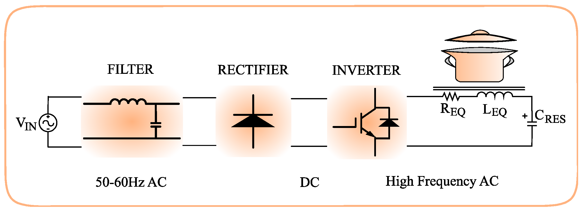
Figure 2.
Single-switch inverter: (a) circuit diagram and (b) circuit schematic.
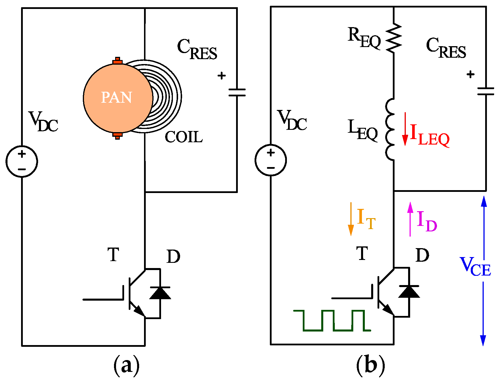
Figure 3.
Current and voltage waveforms of single switch inverter.
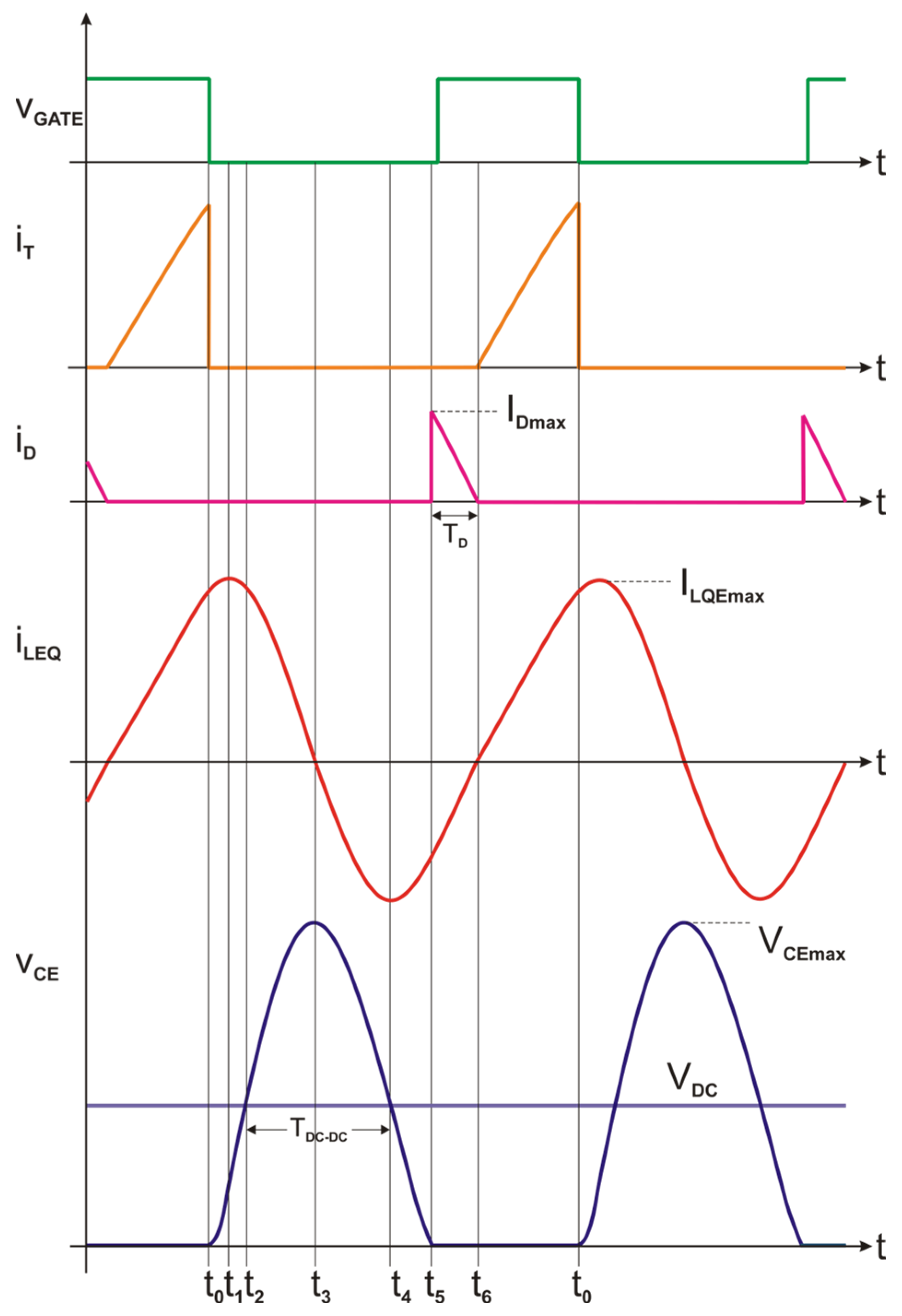
Figure 4.
Circuit operating modes of single-switch inverter.
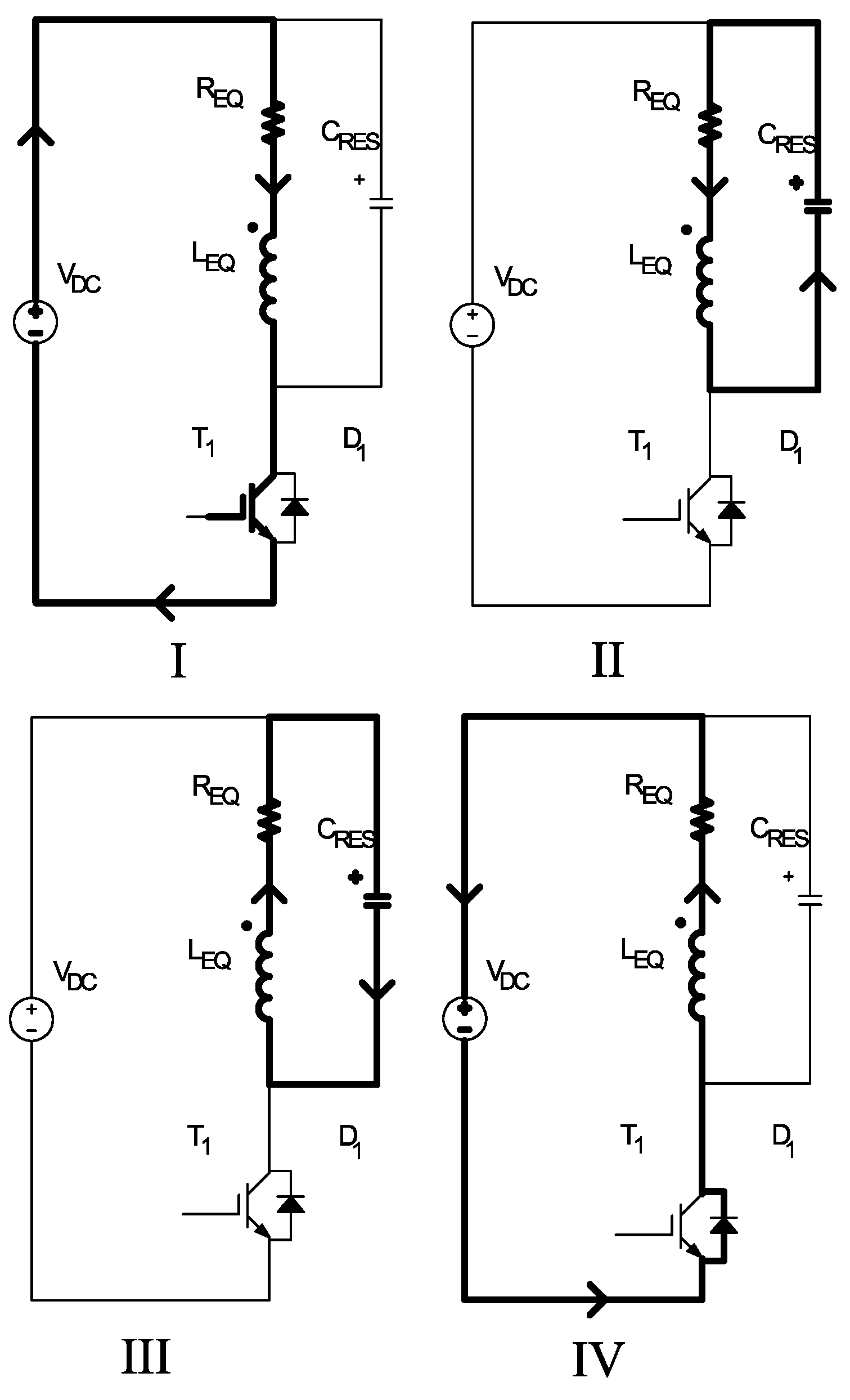
Figure 5.
voltage value variances in PSpice. (a) , , depending on values. (b) , , depending on values. (c) , , depending on values.
Figure 5.
voltage value variances in PSpice. (a) , , depending on values. (b) , , depending on values. (c) , , depending on values.

Figure 6.
current value variances in PSpice. (a) , , depending on values. (b) , , depending on values. (c) , depending on values.
Figure 6.
current value variances in PSpice. (a) , , depending on values. (b) , , depending on values. (c) , depending on values.
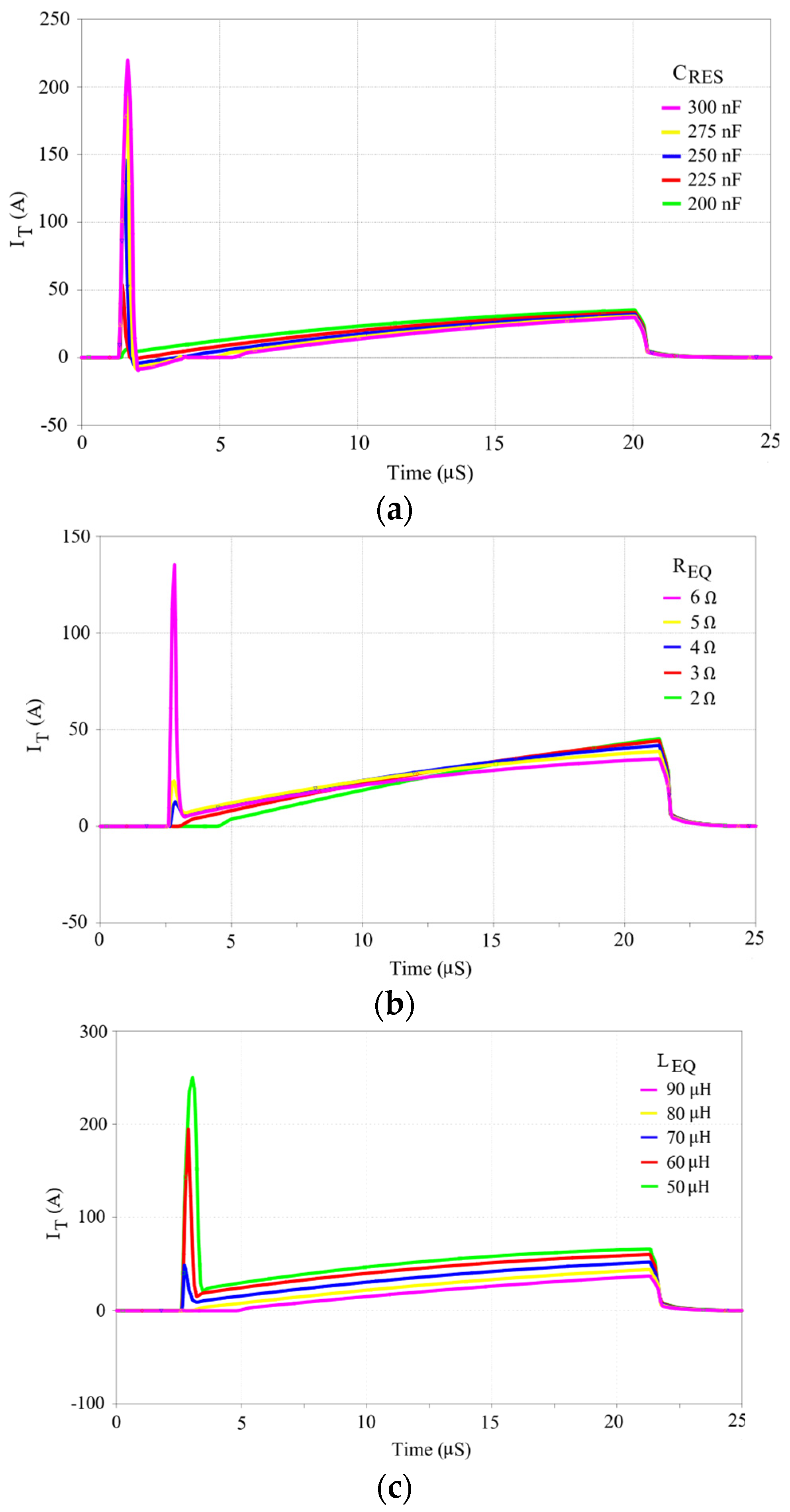
Figure 7.
and switch current as a function of time for the case where the source voltage is the voltage source.
Figure 7.
and switch current as a function of time for the case where the source voltage is the voltage source.

Figure 8.
and switch current as a function of time for the case where the source voltage follows the mains voltage form.
Figure 8.
and switch current as a function of time for the case where the source voltage follows the mains voltage form.

Figure 9.
Switch current as a function of time .
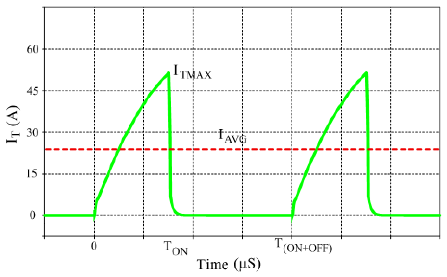
Figure 10.
Input power as a function of time .

Figure 11.
Input voltage as a function of time .
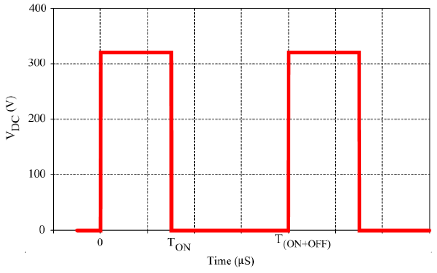
Figure 12.
Flowchart of proposed method to determine , , and .

Figure 13.
Prototype simulation circuit for proposed converter.
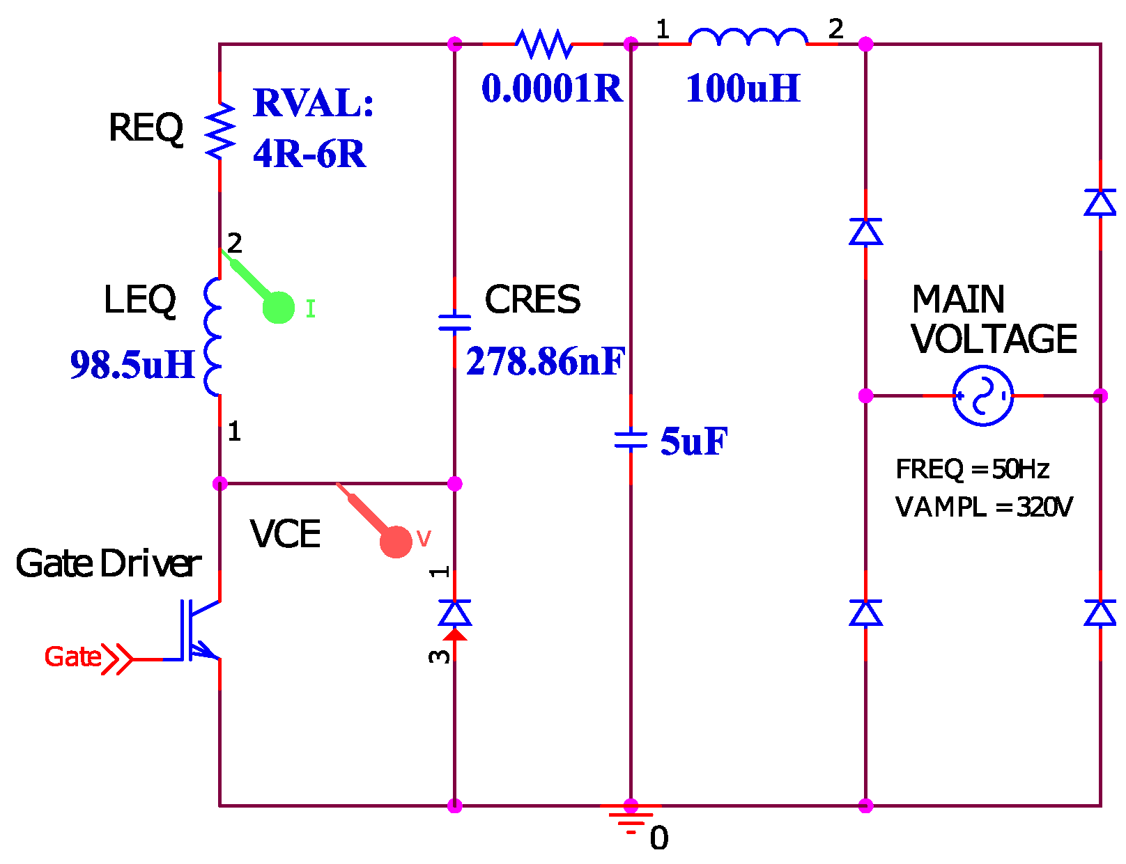
Figure 14.
Coil current and switch voltage for sweeped values as a function of time .

Figure 15.
Coil current, , as a function of time, obtained using the simulation circuit.
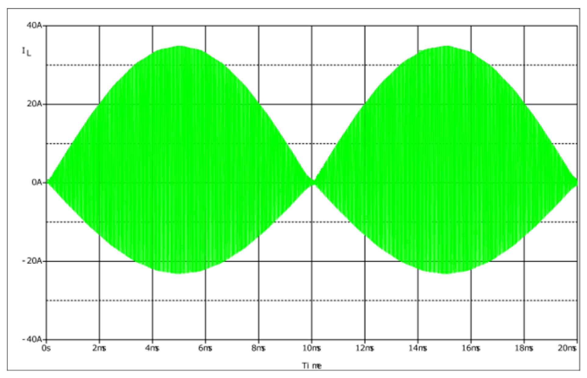
Figure 16.
Switch voltage, , as a function of time, obtained using the simulation circuit.

Figure 17.
General pan models are used with induction cookers.

Figure 18.
Coil current, as a function of time, , obtained using the prototype circuit.
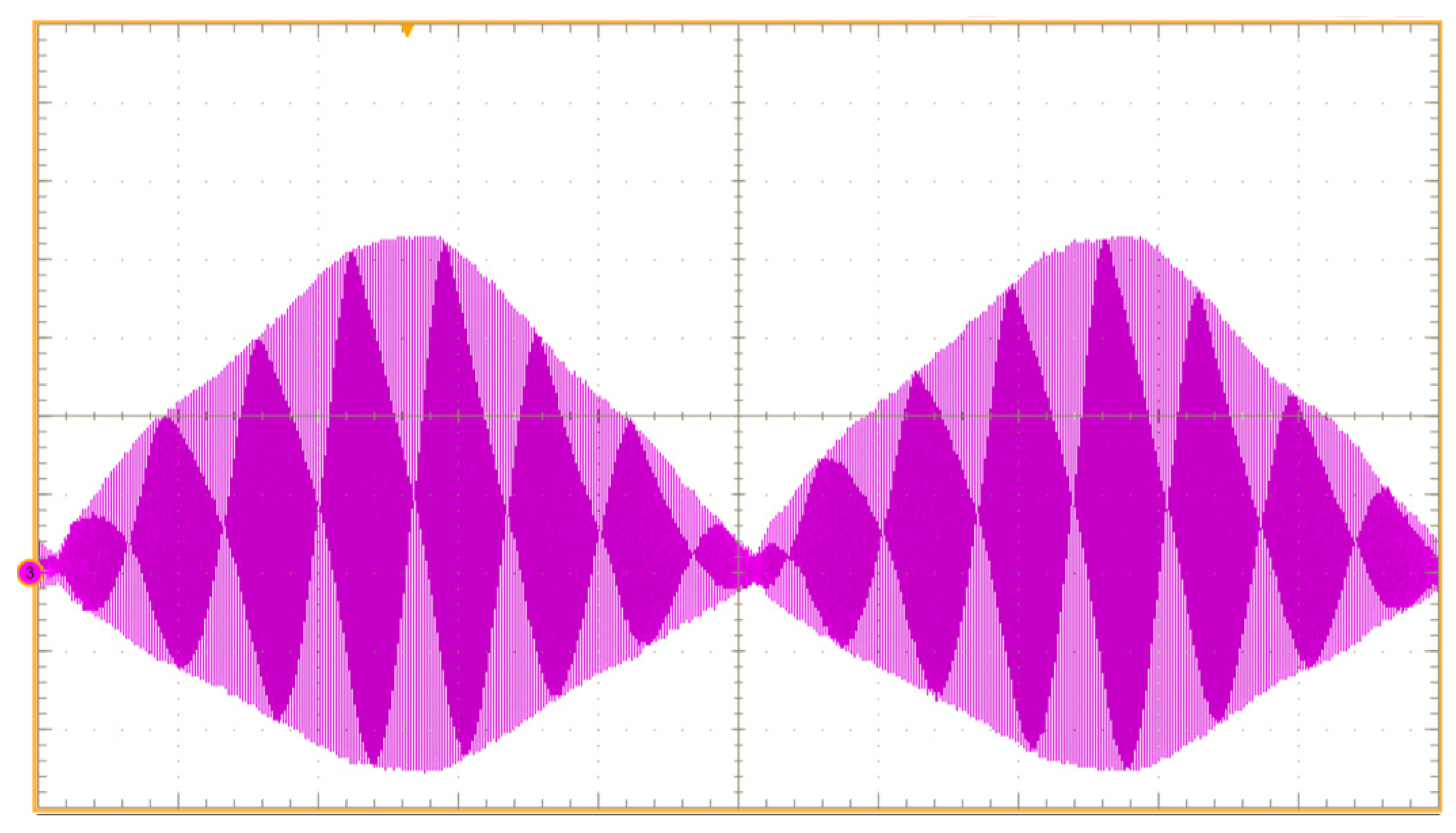
Figure 19.
IGBT collector emitter voltage, as a function of time, obtained using the prototype circuit.
Figure 19.
IGBT collector emitter voltage, as a function of time, obtained using the prototype circuit.

Figure 20.
Detailed waveforms obtained using the prototype circuit. Blue signal: IGBT collector–emitter voltage, (200 V/div). Purple signal: coil current, (10 A/div). Yellow signal: IGBT gate control signal (5 V/div).
Figure 20.
Detailed waveforms obtained using the prototype circuit. Blue signal: IGBT collector–emitter voltage, (200 V/div). Purple signal: coil current, (10 A/div). Yellow signal: IGBT gate control signal (5 V/div).

Figure 21.
Experimental setup.


Table 1.
Calculating circuit parameters.
| Pre-Defined Circuit Parameters | |
|---|---|
| Calculated Circuit Parameters | |
| Calculated Boundary Conditions | |
Table 2.
Simulation circuit results.
| Input Circuit Parameters | Output Boundary Parameters | Output Power | |||
|---|---|---|---|---|---|
Table 3.
Technical specifications of the reference induction coil.
| Parameter | Symbol | Value | Unit |
|---|---|---|---|
| Number of turns | 28 | ||
| External diameter of the coil | 180 | mm | |
| Inner diameter of the coil | 30 | mm | |
| Distance between coil winding and ferrite bars | 4 | mm | |
| Distance between coil winding and pan | 4 | mm | |
| Strand amount of a litz wire | 66 | ||
| Wire diameter of single strand | 0.27 | ||
| Ferrite permeability | 800 | ||
| Equivalent inductance with no load | 110 | µH | |
| Equivalent resistance with no load | 0.12 | ||
| Equivalent inductance with cast iron pan | 89.76 | µH | |
| Equivalent resistance with cast iron pan | 4.21 | ||
| Equivalent inductance with stainless steel pan | 81.81 | µH | |
| Equivalent resistance with stainless steel pan | 3.36 | ||
| Equivalent inductance with silit silargan pan | 69.07 | µH | |
| Equivalent resistance with silit silargan pan | 2.48 |
Table 4.
Experimental circuit results.
| Input Circuit Parameters | Output Boundary Parameters | Output Power | |||
|---|---|---|---|---|---|
Table 5.
Comparison of the calculation, simulation, and experimental circuit results.
| Input Circuit Parameters | Output Boundary Parameters | Output Power | |||
|---|---|---|---|---|---|
Disclaimer/Publisher’s Note: The statements, opinions and data contained in all publications are solely those of the individual author(s) and contributor(s) and not of MDPI and/or the editor(s). MDPI and/or the editor(s) disclaim responsibility for any injury to people or property resulting from any ideas, methods, instructions or products referred to in the content. |
© 2023 by the author. Licensee MDPI, Basel, Switzerland. This article is an open access article distributed under the terms and conditions of the Creative Commons Attribution (CC BY) license (https://creativecommons.org/licenses/by/4.0/).
Share and Cite
MDPI and ACS Style
Ozturk, M. A Simplified Design Method for Quasi-Resonant Inverter Used in Induction Hob. Electronics 2023, 12, 4145. https://doi.org/10.3390/electronics12194145
AMA Style
Ozturk M. A Simplified Design Method for Quasi-Resonant Inverter Used in Induction Hob. Electronics. 2023; 12(19):4145. https://doi.org/10.3390/electronics12194145
Chicago/Turabian StyleOzturk, Metin. 2023. "A Simplified Design Method for Quasi-Resonant Inverter Used in Induction Hob" Electronics 12, no. 19: 4145. https://doi.org/10.3390/electronics12194145
Note that from the first issue of 2016, this journal uses article numbers instead of page numbers. See further details here.