Article

55 nm CMOS Mixed-Signal Neuromorphic Circuits for Constructing Energy-Efficient Reconfigurable SNNs

1
Institute of Microelectronics of the Chinese Academy of Sciences, Beijing 100029, China
2
University of Chinese Academy of Sciences, Beijing 100029, China
3
Key Laboratory of Science and Technology on Silicon Devices, Chinese Academy of Sciences, Beijing 100029, China
*
Author to whom correspondence should be addressed.
Electronics 2023, 12(19), 4147; https://doi.org/10.3390/electronics12194147
Submission received: 22 August 2023 / Revised: 2 October 2023 / Accepted: 3 October 2023 / Published: 5 October 2023
(This article belongs to the Section Microelectronics)

Abstract

:
The development of brain-inspired spiking neural networks (SNNs) has great potential for neuromorphic edge computing applications, while challenges remain in optimizing power-efficiency and silicon utilization. Neurons, synapses and spike-based learning algorithms form the fundamental information processing mechanism of SNNs. In an effort to achieve compact and biologically plausible SNNs while restricting power consumption, we propose a set of new neuromorphic building circuits, including an analog Leaky Integrate-and-Fire (LIF) neuron circuit, configurable synapse circuits and Spike Driven Synaptic Plasticity (SDSP) learning algorithm circuits. Specifically, we explore methods to minimize large leakage current and device mismatch effects, and optimize the design of these neuromorphic circuits to enable low-power operation. A reconfigurable mixed-signal SNN is proposed based on the building circuits, allowing flexible configuration of synapse weights and attributes, resulting in enhanced SNN functionality and reduced unnecessary power consumption. This SNN chip is fabricated using 55 nm CMOS technology, and test results indicate that the proposed circuits have the ability to closely mimic the behaviors of LIF neurons, synapses and SDSP mechanisms. By configuring synaptic arrays, we established varied connections between neurons in the SNN and demonstrated that this SNN chip can implement Pavlov’s dog associative learning and binary classification tasks, while dissipating less energy per spike of the order of Pico Joules per spike at a firing rate ranging from 30 Hz to 1 kHz. The proposed circuits can be used as building blocks for constructing large-scale SNNs in neuromorphic processors.

1. Introduction

Recently mimicking the human brain, neuromorphic hardware that processes information and performs a multitude of functions with low power consumption (~20 mW) and high parallel computing efficiency has emerged, with an increasing interest in its use in edge cloud computing for various applications such as environmental or health monitoring, as well as wearable devices [1,2,3]. Several neuromorphic chips based on spiking neural networks (SNNs) have been developed for Artificial Intelligence (AI) applications [4,5,6,7]. Unlike traditional artificial neural network (ANN) architectures, SNNs closely resemble real biological neural networks by using spike trains as signals for neuromorphic computation. In SNNs, information transmission is encoded based on the temporal relationship between spikes, which greatly improves parallel computing efficiency.
Brain-inspired SNNs are considered to have great potential to support low-power neural computing tasks [8,9,10]. In particular, SNNs have been demonstrated to be an effective algorithmic foundation for efficient processing of temporal signals [11,12]. The complex dynamical properties of these networks play a crucial role in reducing the memory resources necessary for processing, recognizing and classifying extended sequences of temporal data [13,14,15]. Figure 1a depicts a typical SNN comprising neuromorphic unit circuits for pattern recognition. Each input pattern pixel is represented as a random distribution spike train with its frequency proportional to the corresponding pixel value sent to the input layer neurons of the network. Pixel information is encoded by input layer neurons and is transmitted to the output layer composed of Leaky Integrate-and-Fire (LIF) neurons via synapses. As shown at the top of Figure 1b, an LIF neuron performs leaky integration of incoming spikes through input synapses, gradually accumulating them over time and firing spikes only when its membrane voltage reaches the threshold voltage VTH, where VTH denotes the threshold at which the LIF neuron reaches a firing spike. After spiking, the membrane potential of the LIF neuron resets to its resting state. The intelligent source of SNNs is that each synaptic weight can be modified through learning algorithms. Spike Driven Synaptic Plasticity (SDSP) is a biologically plausible learning rule optimized from the well- known Hebbian algorithm mechanism [16]. The weight pull-up process, complying with SDSP regulations, is illustrated in Figure 1b below. Under the control of UP or DN digital signals, the weight undergoes changes until a predetermined voltage threshold (Vthw) is reached, triggering a rapid transition to a stable value. The change in synaptic weight between previous and subsequent moments is indicated as ∆W. Specifically, UP and DN signals are generated by monitoring the firing frequency of postsynaptic neurons and the stimulation time of presynaptic neurons.
Thus, in SNNs’ architecture, signal processing occurs through the following three mechanisms: LIF neurons, synapses and SDSP learning algorithms. Since signal transmission relies on bio-electric impulses and voltage signals, it is presumed that analog/digital circuits are efficient means of implementing neuromorphic circuits [17,18]. Several mixed-signal SNNs have been proposed that include neurons, synapses and spike-based learning algorithms [19,20,21]. However, these circuits have complex structures and high-power consumption in these works. Therefore, designing compact and low-power neuromorphic circuits is crucial for implementing large-scale spiking neural networks. The transistor ratio is crucial for compact and energy-efficient neuromorphic circuits design. The mathematical models of LIF neurons, synapses, and the SDSP learning algorithm dictate the circuit structure and design goals. To balance the charging and discharging speed of the membrane capacitor and minimize leakage current in the design of LIF neuron circuits, it is necessary to increase the transistor ratio of the critical charging branch. The positive feedback charging branch of LIF neurons usually maintains a transistor ratio of more than 6:1, even in larger transistor sizes [19,21]. To meet the mathematical model’s requirements for LIF neurons with exponential dynamic characteristics, all transistors in DPI circuits used to collect synaptic current pulses must maintain the same proportion [18,19,20]. In the design of synaptic circuits, to ensure the adjustability and matching of synaptic time constants, increasing the ratio of transistors controlling synaptic time constants is needed to ensure a wide dynamic synaptic time constant [20,21]. For the design of the SDSP learning algorithm circuit, the transistor ratio of the amplifier needs to be adjusted based on the specific comparison threshold to achieve a more accurate gain.
In this paper, we present a set of mixed-signal neuromorphic circuits that were designed to implement energy-efficient and space-efficient SNNs using 55 nm CMOS technology. In Section 2, we discuss the design strategy for a low-energy analog LIF neuron circuit and illustrate the biophysical complexity of its neural dynamics. A configurable synapse circuit coupled with an optimal SDSP learning algorithm circuit to modify weights is designed. Specifically, the SDSP circuit is capable of precisely regulating synaptic weights to binary states of either 0 or 1 using a bi-stable transconductance amplifier. Moreover, we construct a reconfigurable mixed-signal SNN utilizing the proposed circuits, which allows initial synaptic weights and synaptic attributes to be configured using basic digital circuits. Section 3 shows the test results of the SNN chip fabricated using the 55 nm CMOS process and concludes this summary in Section 4.

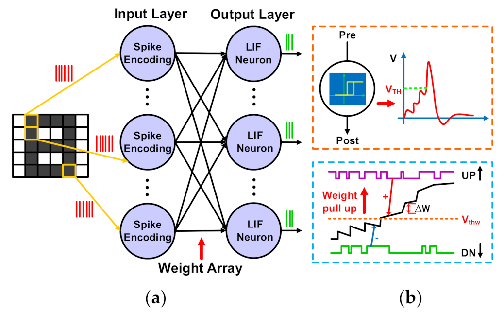
2. Proposed Neuromorphic Circuits and SNN Implementation

In this section, we propose the design of an analog LIF neuron circuit, synaptic circuits and SDSP learning algorithm circuits. We analyze and formulate the advantages of these design methods, and demonstrate biologically plausible dynamic behaviors of these circuits. To build a reconfigurable mixed-signal SNN using these neuromorphic circuits, we employ asynchronous digital circuits to assign routing for synaptic arrays.

2.1. Analog LIF Neuron

The LIF neuron model has gained popularity as it is thought to capture many properties of biological neurons, while requiring fewer and less complex differential equations compared to more complex conductance-based models such as Mihalas–Niebur and Izhikevich [22,23]. LIF neurons’ computational efficiency and compact size make them valuable choices for constructing large-scale neuromorphic processors [24,25]. However, previously, LIF neurons required a significant amount of bias voltages or currents to configure circuit properties and resulted in large footprints and high energy consumption. The voltage amplifier and the tau-cell LIF neurons presented in [24,25] are considered to be efficient embodiments of biological neurons; however, their power consumption may not be as low as possible. The differential pair integrator (DPI) and low-pass filter (LPF) LIF neurons are not regarded as compact cases in previous studies [26,27]. Time-domain LIF neuron circuits feature intricate structures, including the integration of digital logic circuits that serve as spike generators [28,29]. This increases the circuit area cost and design complexity, while also resulting in higher dynamic circuit power consumption.
We propose an analog LIF neuron circuit. The purpose of proposing this neuron is to provide a low energy and compact structure utilizing highly efficient analog circuits. Figure 2 shows the neuron circuit structure. To ensure biologically plausible dynamics of neurons and synapses in SNN hardware design [30], a DPI circuit was used as an input current integrator to the neuron. Specifically, the DPI circuit avoids transistors with bulk source connections and is unaffected by any mismatches between its current sources, resulting in a smaller silicon area and lower power consumption. Therefore, it provides a compact and low-power solution. Unlike LIF neuron circuits that use transconductance amplifiers that are sensitive to supply variations [31,32], our design employs a current-based positive feedback amplifier to control spike generation. This helps to limit the input voltage swing and reduce sensitivity to supply variations, while also decreasing dynamic power consumption of the neuron circuit.
As seen, the neuron comprises an input DPI circuit (ML1–3) used as an LPF, which models the leakage conductance of the neuron; a Na+ block (MN1–7) models the neuron’s Sodium (Na+) activation and inactivation channels and includes an amplifier that generates spike events with positive feedback based on current; a K+ block forms two first-order low-pass filters to model the effect of potassium conductance, resets the neuron and implements a refractory period functionality (MK1–4); a AHP module (MA1–2) in K+ models the Calcium-dependent after-hyperpolarization Potassium currents observed in neurons, producing the spike-frequency adaptation mechanism. The above simplest highly efficient analog circuitry approaches lead to a low-energy biologically plausible neuron.
The DPI circuit functions as a low-pass filter, generating exponential dynamics in response to input currents that integrate into the membrane capacitance Cmem. The filter gain can be adjusted by Vthr. Transistor ML3 acts as a fixed leakage transconductance for this neuron that satisfies biologically plausible time constants, and leakage current Ileak can be controlled by bias voltage Vleak. Integrating more input current into Cmem leads to an increase in membrane voltage Vmem. The Vmem rises to a certain threshold; the current-based amplifier (MN1–3) is activated and generates a positive feedback current Ipf to rapidly charge the Cmem. The voltage at node Vo1 then decreases significantly and a pulse is generated by the inverter MN4–6. With each spike, the capacitor Cref is charged step by step through the transistor MK3 and the membrane voltage Vmem is reset to the resting potential as long as the voltage Vu is high enough to turn on transistor MK1–2. This effectively establishes the refractory period function of the neuron. Moreover, the leakage current Iref is progressively decreased as the capacitor Cref is charged, resulting in a longer refractory period and a lower firing frequency. The bias voltage Vref is also used to adjust the duration of the refractory period. However, the capacitor Cref is slowly discharged through the leakage path MA1–2 (representing the calcium transconductance after-hyperpolarization current Iadp [21]), ultimately maintaining a stable value for the current Iref, which also keeps the voltage Vu at a dynamically stable value. Consequently, the firing frequency of the neuron reaches a stable point and has a lower value than its initial frequency. This process effectively implements the frequency adaptation mechanism. Based on the above analysis, it is evident that the circuit operates by consuming power only during spike generation, minimizing power loss during idle periods.
The computational mode of the LIF neuron is derived from the adaptive neuron described in [33] as two coupled differential equations that follow.
C d V d t = G l k ( V R L ) + G l k Δ T e V V T H Δ T h + I
τ h d h d t = w ( V G l k ) h
where C is the membrane capacitance, V is the membrane potential, Glk is the leakage conductance, RL is the resting potential, I is the input current (i.e., synaptic current) and h is the after-hyperpolarization adaptation current. The term ∆T represents the threshold slope factor, VTH represents the activate threshold potential of the neuron, w is the adaptation threshold and τh is the adaptation time constant.
The current of the charge–discharge branch of the membrane capacitance serves as the control variable of the neuron circuit. Hence, the currents Imem and Iahp correspond to the V and h variables of the computational model described in Equations (1) and (2), respectively. By applying Kirchhoff’s current law on the membrane potential node Vmem, the circuit’s behavior can be determined as
C m e m d d t V m e m = I M L 2 I l e a k I a h p + I p f
The gain of the DPI circuit can be adjusted precisely with the bias voltage Vthr. Adopting the trans-linear principle to the DPI circuit, as referenced in [30], we employ uniform transistor parameters and use ultra-low leakage currents where IleakIin, and the circuit’s dynamics can be expressed as
C m e m d d t I m e m = I l e a k I m e m + I m e m I p f I l e a k + I l e a k ( I i n I a h p )
C a d p I a d p d d t I a h p = I a h p I a d p
where I m e m I p f / I l e a k is a positive feedback current contributed by the DPI block and the Na+ block, which can be approximated as an exponential function of Imem; Iadp is the slow variable as the adaptation coefficient responsible for spike-frequency adaptation mechanisms. Therefore, the circuit depicted in Figure 2 and described by Equations (4) and (5) represents a generalized conductance-based LIF neuron model, which takes the form of an adaptive exponential LIF neuron model, as detailed in [33].

2.2. Configurable Synapse and SDSP Learning Algorithm

The synaptic transmission converts presynaptic voltage pulse signals into postsynaptic currents that are injected into the target neuron’s membrane with a strength governed by synaptic weight. Synaptic weight translates fast presynaptic pulses into long-lasting postsynaptic currents with intricate temporal dynamics, while theoretically simplifying this process with linear exponential temporal characteristics [34]. In Very Large-Scale Integration (VLSI) SNN architectures, a single postsynaptic neuron circuit integrates currents from multiple synapses. The postsynaptic neuron performs a weighted sum of input signals, resulting in postsynaptic potentials that rise with stronger excitatory synapse activity and fall with stronger inhibitory activity. As such, one of the primary requisites for synaptic circuits is compactness to ensure maximum integration of synapses on the chip, using minimal silicon area. However, implementing synaptic integrator circuits with linear response characteristics and time constants comparable to the time constant of the neuron’s membrane potential may demand significant silicon real estate. Therefore, designing compact linear synaptic circuits that model the functional properties of biological synapses remains a challenging task that continues to be actively pursued.
Various synaptic circuit designs have been proposed, with different trade-offs between functionality, complexity of temporal dynamics and circuit/layout size [34,35,36]. Some proposed circuits utilize floating-gate devices or limit the dynamic range of the signal to mimic the biophysical characteristics of synaptic channels [37,38]. Here we propose synaptic circuit features with a wide and linear exponential dynamic range. Figure 3 illustrates a schematic of the synaptic circuit. To meet SNN requirements with a compact design, excitatory and inhibitory synapses are integrated together. This design provides attribute configuration as a novel feature for synaptic circuits and has a smaller circuit area compared to the State-of-the-Art designs that use oscillator-based transconductance synaptic circuits [39].
The excitatory (M6–7) and inhibitory (M9–10) synapses are voltage-controlled current sources that are activated by a presynaptic pulse (Pre_spk) and weight (Vw). The attributes of the synapses can be configured according to actual needs through the digital signal Conf to control transistors M5 and M8. Transistor M1 acts as a constant current source to the linearly charged capacitor Csyn, while M6 generates an excitatory current exponentially dependent on the Vsyn node and M7 adjusts the magnitude of the excitatory current via bias voltage Vexc. Transistors M9–10 generate inhibitory synaptic exponential current to discharge neurons’ membrane potentials. Taking the excitatory synapse as an example, based on the linear transmission principle, the synapse obeys the following dynamics:
C s y n I τ d I s y n d t + I s y n = I w I τ
where Isyn is the synapse output current; Iτ and Iw is a current set by Vτ and Vw, respectively. The synapse time constant can be controlled by capacitor Csyn and current Iτ. To increase the time constant of the circuit, it is necessary to increase the size of capacitors or decrease the Iτ current. To avoid the large area requirements brought about by increasing capacitor sizes in the 55 nm technology, we adjust the W/L ratio of M1 to achieve an optimal exponential current time constant for LIF neurons.
A primary feature of biological synapses is their ability to display various forms of plasticity. Plasticity mechanisms induce enduring modifications in the synaptic efficiency of single synapses, enabling the storage and learning of input stimulus statistics. Plasticity mechanisms that increase synaptic weights are termed as long-term potentiation (LTP) mechanisms, while those that decrease synaptic weights are termed as long-term depression (LTD) mechanisms [40]. To realize the mechanism of synaptic plasticity, many spike-based models of synaptic plasticity learning algorithms are proposed, such as Spike-Timing Dependent Plasticity (STDP), Spike-Driven Synaptic Plasticity (SDSP), etc. Several STDP models have been proposed in computational neuroscience for classifying spatio-temporal spike patterns [41,42]. However, emerging evidence indicates that spike-timing-based learning algorithms alone are insufficient to explain all the phenomena observed in neurophysiological experiments [43]. These algorithms also exhibit poor memory retention performance and necessitate supplementary mechanisms to grasp spike-time correlations and input pattern mean firing rates [44]. For these reasons, we opted for implementing the spike-driven synaptic plasticity mechanism proposed by [16], as it has demonstrated the ability to mimic various biological phenomena and exhibits performance features that match those of the latest machine learning techniques [16,41,42]. This algorithm updates synaptic weights not only based on spike-timing, but also considers the timing of presynaptic spikes, the current state of membrane potential of the post-synaptic neuron and its recent spiking history behavior. The schematic of the proposed revised analog/digital SDSP learning algorithm circuits is shown in Figure 4. Figure 4a is a component of the SDSP circuit used to update weights through control signals received from the submodule, as depicted in Figure 4b.
In Figure 4a, MH1–H6 comprise a spike-triggered weight update block. When spikes from presynaptic neurons are received, it increases or decreases synaptic weight Vw depending on the digital signals UP and DN generated downstream by the postsynaptic neuron. Up and down jumps height of weight can be adjusted by changing the Vu and Vd signals. A bi-stability weight refresh circuit comprised of MB1–B11 is a wide-range positive-feedback transconductance amplifier with a low slew rate that continuously compares the Vw node with the threshold voltage Vthw. If Vw > Vthw, the amplifier slowly drives the Vw node toward the positive rail; otherwise, it actively drives it toward the ground. The drift rates to high and low states can be tuned with bias voltage WU and WD, respectively. The bi-stable property effectively implements the LIP and LTD mechanisms’ process for weight updates and eliminates the problematic requirement of storing precise analog variables for synapses at long time scales. In addition, the INIT block MW1–4 can be used to set the initial state of the synapse weight: when the write (PW) signal stays high, the weight Vw is shorted to Vdd or toward the ground according to bit b2.
Figure 4b shows the postsynaptic learning control circuits of the SDSP learning algorithm for evaluating weight updates and “stop-learning” conditions. The spikes from the postsynaptic neuron are integrated by MC1–C3 into the capacitor CCa, generating a voltage VCa that reflects postsynaptic calcium concentration and serves as an indicator of recent spiking activity of the neuron, and compares this voltage VCa to three threshold voltages Kup, Kmid and Kdw. In parallel, the membrane potential Vmem(tpost) of the neuron is compared to a set threshold θmem using a voltage comparator. The comparison results determine UP and DN, such that synapse weights are adjusted whenever a presynaptic spike Pre_spk reaches the weight update module shown in Figure 4a.
The weight update and stop-learning rule can be governed by the following equations, assuming the arrival of each presynaptic spike:
V w = V w + Δ w + if V m e m ( t p o s t ) > θ m e m and K d w < V C a < K u p V w = V w Δ w if V m e m ( t p o s t ) < θ m e m and K d w < V C a < K m i d
where the factor ∆w+ and ∆w determine the amplitude of the weight Vw increases and decreases; Vmem(tpost) represents the membrane potential of the postsynaptic neuron when have presynaptic spike arrives; θmem is a set thresholds for determining whether the weight should be adjusted up or down; and the thresholds Kup, Kmid and Kdw determine the conditions under which weights can be increased, decreased, or not updated. If none of the above equation conditions are met, ∆w+ and ∆w are nullified by setting UP to Vdd and DN to 0. This stop-learning mechanism significantly enhances the system’s ability to generalize by preventing overfitting once the input pattern has been learned [16,19,21].
Alongside the immediate weight updates, the weight Vw is continuously drawn toward one of two stable states as mentioned in Figure 4a, determined by if it is below or above a predetermined threshold Vthw as follows:
d d t V w = Δ J + if V w > V t h w and V w < W m a x d d t V w = Δ J if V w < V t h w and V w < W m i n
where ∆J+ and ∆J represent the weight drive rates towards its upper and lower bounds, respectively, while Wmax and Wmin represent the upper (i.e., Vdd) and lower bound (i.e., ground), respectively.
As already mentioned, the synapse can be configured with specific characteristics using basic digital circuit combinations. The schematic of the synapse configuration element is shown in Figure 5.
It consists of a signal flip-flop to store the configuration bit b1, a three-state buffer for reading out the synaptic state and four logic gates for combining the incoming digital signals. The signals Xconf and Yconf are derived from a horizontal and vertical configuration decoder, respectively, to select the synapse that needs to be configured. Bit b1 can be used to configure the synapse contact as either excitatory or inhibitory by setting the value of the digital line Conf. Setting Conf to 0 enables the excitatory branch, while setting it to 1 enables the inhibitory branch of the synapse depicted in Figure 3. CLK clock signal is essential to ensure reliable data transmission of bit b1 and it also plays a crucial role in generating write signals PW and nPW to activate the INIT circuit that sets the initial state of the synapse according to bit b2 (see Figure 4a). In an SNN, the two bits b1 and b2, along with CLK signals, can be broadcasted to all synapses, and the selection lines Xconf and Yconf enable one synapse at a time. The three-state buffer’s input is connected to the Vw_state line and drives a digital output pin to readout the real-time digital state of synapse weights, which is beneficial for monitoring the status of SNNs during training. The configurability of the synapse is an innovative feature for constructing reconfigurable SNNs.

2.3. Reconfigurable SNN Implementation

Once the basic neuromorphic unit circuits including the compact energy-efficient neuron were built, we configure exponential feature synapse and highly biomimetic SDSP with the stop-learning function. We constructed a reconfigurable mixed-signal SNN based on these neuromorphic unit circuits. The structural diagram of the SNN is shown in Figure 6a. It comprises four presynaptic neurons as the input layer, two postsynaptic neurons as the output layer and two teacher neurons as the supervisory signals for weight updates. Each neuron in the input layer has a synapse to receive and transmit external stimulus signals. The presynaptic and postsynaptic neurons are fully connected by eight synapses, including eight SDSP weight learning algorithm circuits. In addition, the output layer of the SNN employs a Winner Take All (WTA) connection rule to create competitive interactions among the output neurons, where neurons with first firings suppress all other neurons to win the competition. Competition renders the output of a single neuron reliant on the collective activity of all neurons in the SNN, rather than just its own input. The synapse matrix can be flexibly configured through configurable elements, and each synapse weight is routed to the weight output bus via a three-state gate to read the SNN’s real-time digital weight status updates.
The SNN is fabricated using the 55 nm CMOS process; the chip micrograph is shown in Figure 6b. The chip has an area of 0.9 × 1.1 mm2, with each neuron occupying 264 µm2 and the learning control circuits occupying 300 µm2. The synapse and weight updating circuits are integrated and cover an area of 514 µm2. The chip also includes two 2–4 decoders and other digital logic gate circuits as peripheral signal transmission interfaces.

3. Chip Measurement Results

The chip measurement setup is shown in Figure 6c. The measurement system consists of a Xilinx Artix-7 AX7035 FPGA board that receives command packets via a USB interface and a PCB test substrate with the chip installed onto it via LQFP sockets. The core circuit of this chip operates at a power supply of 1.2 V, while the PAD requires a power supply of 1.8 V. The LIF neurons, plastic synapses and SDSP learning algorithm circuits in the SNN are controlled by externally biased voltage signals. Input and teacher neurons receive external digital spike sequences as stimulation signals, transmitted via plastic synapses to stimulate the output neurons for results. The configuration unit and peripheral communication module receive external digital signals to configure the network. SNN’s output signals consist of four analog and five digital signals. All analog bias voltages in the test are generated with resistive dividers, and all digital input stimulus signals are produced with the FPGA and loaded into the chip. The digital signal outputs are acquired utilizing the FPGA’s Integrated Logic Analyzer (ILA core) and observed as a waveform on the Vivado GUI through a downloader that implements JTAG interface to the USB interface data conversion, while the analog signal outputs are captured using a digital oscilloscope with a sampling rate of 5 GHz.

3.1. LIF Neuron Behavior Testing

To show the dynamic behaviors of neurons through the combination of synaptic circuits, we stimulate a chosen neuron in the SNN through excitatory synapses, while sweeping different bias parameters for the neuron. Figure 7 shows the test results of the neuronal refractory period and the frequency adaptation mechanism.
At the top of Figure 8, the membrane potential (Vmem) variation of the neuron during stimulation of an excitatory synapse with a presynaptic input spike train average frequency of 500 Hz is shown. Adjusting the bias voltage Vref in the K+ block of Figure 2 can achieve different refractory periods. Larger voltage Vref results in a longer refractory period for the neuron. Due to the voltage Vu remaining at a sufficiently high level, there is enough leakage current Iahp to discharge the neuronal membrane potential to its resting state without being affected by input stimulation. Modifying the refractory period of neurons allows for wide-ranging frequency modulation and shows great potential for larger spiking neural network systems [18,19,20,21]. The bottom of Figure 8 shows the spike-frequency adaptation behavior obtained by appropriately tuning the voltage parameters in the AHP block of Figure 2, while stimulating the neuron by a synapse applies a constant step voltage and is shown as the pink trace at the bottom. As seen, the neuron is initially firing at a high rate and gradually reaches stability at a lower rate compared to the initial firing. This adaptive frequency process reduces the firing rate to conserve energy for neurons.
The variation in input intensity impacts neuronal firing rates. We recorded the firing response of a neuron to varying intensities of an input excitation, ranging from 50 Hz to 2 kHz, as depicted in Figure 8. For weaker stimuli, such as below 100 Hz, it is difficult for neurons to generate responses due to the inability to reach the firing threshold. This is a manifestation of the intrinsically conditioned response of the neuron. As the intensity of the input stimuli increases, the firing rate of the neuron gradually increases and then reaches saturation at approximately 1 kHz. As a result, the proposed neuron exhibits a wide firing output (ranging from about 30 Hz to 1 kHz), ensuring its compatibility with large-scale SNNs such as [14,18,19,20,21] those that share similar firing rates. The proposed neuron operating at the 30 Hz–1 kHz frequency range is sufficient for real-time SNN applications for natural signals such as speech, human characteristics, biological signals, and various environmental signals that typically have time constants ranging from milliseconds to seconds in SNN processing [19,20,21].

3.2. SDSP Learning Algorithm Testing

In this section, we present the SNN measurements that implement the SDSP learning mechanism described in Section 2.2. We choose a presynaptic and postsynaptic neuron, along with their connecting synapses and SDSP circuits, as a complete signal flow. We generate Poisson-based spike trains for presynaptic input stimulation, while the postsynaptic neuron is driven by a teacher neuron acting as a teacher signal in a supervised learning condition. The teacher neuron is stimulated by Poisson-based spike trains generated with FPGA. The Poisson nature of the spike trains used in this way is essential for implementing stochastic learning by providing the necessary variability [45, 46].
Figure 9 shows the experimental results of stochastic learning that highlight the operational features of both synapse and neuron learning circuits. The bottom trace represents presynaptic input spikes (500 Hz Poisson spike trains); the second trace from the bottom represents bi-stable weight updates (node Vw in Figure 4a); the third trace represents the membrane potential of the postsynaptic neuron; and the upper two traces represent digital control signals (UP and DN) that determine whether to increase, decrease or maintain Vw at its current value. Weight updates occur when the arrival of presynaptic spikes and the calcium concentration of the postsynaptic neuron is within the appropriate range, as discussed in Section 2.3 on postsynaptic learning control circuits. Based on the calcium concentration signal, the digital UP (active low) and DN (active high) signals turn on or off to enable the weight update mechanism. The weight is adjusted to increase or decrease depending on the postsynaptic membrane potential relative to the membrane threshold (refer to highlighted weight updates at t = 1.74 s and t = 1.97 s). The weight is slowly driven toward the low or high stable states, determined by whether it falls below or above the weight threshold Vthw.

3.3. Pavlov Associative Learning Experiment and Binary Classification Task Testing

The above experiments demonstrate the biological similarities between the behaviors of the neuron and the properties of the SDSP learning circuits implemented in the SNN chip. To validate the applicability of this reconfigurable SNN in specific tasks, we conducted both associative learning experiments and classification task experiments, respectively. In the associative learning experiment (known as Pavlov’s dog [47]), we select two input layer neurons for the sensory decision and one output layer neuron for the association decision. The results of the associative learning experiment are shown in Figure 10.
As seen, the time from 0 to 0.6 s represents the initial configuration period of the network prior to experimentation. X0 and X1 are outputs from the row decoder that select the desired synapses in the network as configurations, while CLK, b1 and b2 are configuration signals used to set the attribute and initial weights of the selected synapses (see Section 2.3 for details). Here, the chosen synapses were configured as excitatory through b1. The initial weight of the synapse connected to sensory neuron 2 was set to high by b2 at 0.1–0.3 s, while the synapse connected to sensory neuron 3 was set to low by b2 at 0.3–0.5 s. For sensory neurons 2 and 3, there is the same input stimulus as for the Poisson spike trains at 300 Hz. Before learning, the “salivation” neuron only responded to stimuli from the “Sight of Food” neuron 2. By co-stimulating “Sight of Food” neuron 2 and “Sound of Bell” neuron 3, the synapse between neuron 3 and the decision neuron was potentiated with the SDSP learning algorithm. After learning, when the stimulus from the “Sound of Bell” neuron 3 was used alone, the “salivation” neuron was excited and responded to neuron 3, thus establishing an association between the conditioned (“Sight of Food” neuron 2) and unconditioned (“Sound of bell” neuron 3) stimuli. The weight variation of associative learning was monitored in real-time and recorded as the W_State signal.
Associative learning is crucial in understanding how the brain connects events and for enhancing the effectiveness of neural networks in certain tasks. The successful implementation of associative learning highlights the SNN chip’s proficiency in performing intricate learning tasks. Figure 11 shows the results of a binary classification task experiment.
In this classification experiment, two patterns (pattern 1 and pattern 2) consisting of distinct pixels are loaded onto the network, where black pixels represent the stimulation from a 200 Hz Poisson spike train, while white pixels represent no stimulation. Input layers of neurons 1 and 3 correlate to pixels 1 and 3, while neurons 2 and 4 correlate to pixels 2 and 4. Output layer neurons 1 and 2 represent the spike outputs of patterns 1 and 2, respectively. During the initial configuration period of 0–0.9 s the synapse connecting the input neuron 1 and output neuron 2 is configured as inhibitory with b1 at 0.2–0.3 s; similarly, the synapse connecting input neuron 4 and output neuron 1 is configured as inhibitory with b1 at 0.7–0.8 s, while all other synapses are configured as excitatory with b1 (high level); the initial weights of all synapses is set to 0 via b2.
Firstly, pattern 1 is inputted to the network and the output neuron 1 has no response. With the guidance of teacher neuron 1 (a 300 Hz Poisson spike train) and co-stimulation of pattern 1, connections are established between input neurons 1 and 3 with output neuron 1, resulting in a response to pattern 1. This also means that the weights Vw11 and Vw13 (see Figure 6a) are updated from low to high with the SDSP learning algorithm, as can be seen from the weight output signal W_State at 2.0–2.1 s for Vw11 and 2.4–2.5 s for Vw13. Establishing a connection between pattern 2 and output neuron 2 follows the same process as pattern 1. The weights Vw22 and Vw24 (see Figure 6a) are updated from low to high with the SDSP learning algorithm, as can be seen from the weight output signal W_State at 2.3–2.4 s for Vw22 and 2.7–2.8 s for Vw24. After establishing connections between two patterns and output neurons, when the stimulus from pattern 1 was used alone, output neuron 1 was excited and responded to pattern 1. Conversely, while the stimulus from pattern 2 was used alone, output neuron 2 was excited and responded to pattern 2, and the binary classification task was effectively performed using the SNN chip. Integrating multiple SNN chips together enables networks to handle complex application tasks, as demonstrated in previous studies [20,21,48,49,50].
In this design, the indicator for evaluating the classification accuracy of SNNs in binary classification tasks is the change in synaptic weight after SNN training. After training with the standard binary task, the weight distribution of the 4 × 2 synaptic arrays in SNNs is as follows: the synaptic weights between the pre- and post-neurons corresponding to black pixels are at a high level, while the synaptic weights between the pre- and post-neurons corresponding to white pixels are at a low level. To evaluate the classification accuracy of SNNs in binary classification tasks, we applied varying degrees of noise to two patterns (i.e., white pixels were subjected to lower frequency Poisson spike trains, ranging from 10 Hz to 50 Hz), and the two patterns were divided into 5 groups for a 10-training epoch. After each epoch, the weight changes of 4 × 2 synaptic arrays in the network are counted and compared with the standard synaptic weights. After training, the accuracy of the binary classification network can be evaluated by determining the proportion of synaptic weights in the network that are the same as the standard synaptic weights. Figure 12 presents the binary classification accuracy versus training epoch statistics for the SNN, comparing simulation and testing results.
During the initial stage (1–4), the SNN began to learn the two noise patterns, resulting in a relatively low accuracy due to the significant difference between the trained weights and standard weights. In the middle stage (4–8), as the SNN continues to associate and learn, the network gradually adjusts the weight matrix toward the standard weight via inhibitory synapses, leading to an increase in accuracy. In the later stage (8–10), the SNN further learns to associate the two noise patterns and inhibits most of the synaptic weight differences caused by the noise signals, resulting in a stabilized accuracy. Through testing, the SNN achieves an accuracy of approximately 91.4% in recognizing the two noise patterns, while the simulation accuracy reaches 92.8%. However, a possible reason for the deviation between the testing and simulation accuracy could be the weighting testing error caused by the noise and leakage current in the testing substrate.

3.4. Energy per Spike

To evaluate the energy efficiency of the SNN, the energy consumption per spike is a critical figure of merit (FoM) [21,24]. In the binary classification experiment, we measure the firing frequency of single neurons and calculate the energy per spike relative to the firing rate. The energy per spike equals
E n e r g y F r e q T i m e = P a v e T i m e F r e q T i m e = P a v e F r e q
where Energy is the product of average power consumption (Pave) and excitation time (Time) that is represented as (Pave·Time), and Freq is the spiking frequency. Figure 13 illustrates that the energy per spike declines from hundreds of pJ for lower frequencies to tens of pJ for higher frequencies (as reference at 92.6 pJ@300 Hz). This occurs as inverters operate at higher levels of gain in the lower frequency range, owing this to a slower charging of the membrane voltage Vmem input when compared to higher frequency operation.
Table 1 compares the features of our designed circuit with other configurable circuits applied to neuromorphic systems [48,51] and circuits with the same process [52]. Compared to a 180 nm circuit design [48], our design exhibits superior energy efficiency with 483 pJ@30 Hz (refer to Figure 13) than the reference design 883 pJ@30 Hz, while also occupying a smaller circuit area. Moreover, the circuits used in [52] and our work have the same process, and it can be noted that our design offers significant advantages in both the area and power consumption. Compared to a more advanced 28 nm switched capacitor design [51], our design has a power efficiency that is approximately lower than two orders of magnitude. However, to achieve more complex biomimetic dynamic behaviors, our design requires a larger capacitance and transistor size, resulting in a larger circuit area relative to [51].

4. Conclusions

In this paper, we present a set of digital/analog neuromorphic circuits and implement a reconfigurable mixed-signal SNN fabricated with 55 nm technology. By measuring this SNN chip, the analog neuron can achieve stable refractory period adjustable behavior and a spike-frequency adaptive mechanism, and exhibits a wide firing rate ranging from about 30 Hz to 1 kHz. Synapses are equipped with digital configurable elements that enable excitation and inhibition configuration, as well as initial weights settings. The SDSP learning algorithm circuits employ a transconductance amplifier to achieve a stable binary weight output. We perform Pavlov’s dog association learning experiment and binary classification tasks by configuring synaptic arrays of the SNN chip. Compared to other configurable neuromorphic circuit designs with a mixed-signal, our proposed designs are more cost-effective and energy-efficient. Therefore, the proposed circuits can be used as building blocks for constructing large-scale SNNs in neuromorphic processors to efficiently handle complex application tasks.

Author Contributions

Conceptualization, study design, chip tests, data analysis, data interpretation and writing, J.Q.; literature search and processing of graphics, J.Q. and Z.L.; testing guidance, C.Z.; resources, J.L.; writing—review and editing, B.L. and J.L. All authors have read and agreed to the published version of the manuscript.

Funding

This research received no external funding.

Data Availability Statement

Data used in this article will be made available upon request from the corresponding author.

Conflicts of Interest

The authors declare no conflict of interest.

References

  1. Grollier, J.; Querlioz, D.; Camsari, K.Y.; Everschor-Sitte, K.; Fukami, S.; Stiles, M.D. Neuromorphic spintronics. Nat. Electron. 2020, 3, 360–370. [Google Scholar] [CrossRef]
  2. Indiveri, G.; Liu, S.-C. Memory and Information Processing in Neuromorphic Systems. Proc. IEEE 2015, 103, 1379–1397. [Google Scholar] [CrossRef]
  3. Monroe, D. Neuromorphic computing gets ready for the (really) big time. Commun. ACM 2014, 57, 13–15. [Google Scholar] [CrossRef]
  4. Milde, M.B.; Blum, H.; Dietmüller, A.; Sumislawska, D.; Conradt, J.; Indiveri, G.; Sandamirskaya, Y. Obstacle Avoidance and Target Acquisition for Robot Navigation Using a Mixed Signal Analog/Digital Neuromorphic Processing System. Front. Neurorobotics 2017, 11, 28. [Google Scholar] [CrossRef] [PubMed]
  5. Liu, B.-C.; Yu, Q.; Gao, J.-W.; Zhao, S.; Liu, X.-C.; Lu, Y.-F. Spiking Neuron Networks based Energy-Efficient Object Detection for Mobile Robot. In Proceedings of the 2021 China Automation Congress, Beijing, China, 22–24 October 2021. [Google Scholar] [CrossRef]
  6. Furber, S.B.; Galluppi, F.; Temple, S.; Plana, L.A. The SpiNNaker Project. Proc. IEEE 2014, 102, 652–665. [Google Scholar] [CrossRef]
  7. Davies, M.; Srinivasa, N.; Lin, T.-H.; Chinya, G.; Cao, Y.; Choday, S.H.; Dimou, G.; Joshi, P.; Imam, N.; Jain, S.; et al. Loihi: A Neuromorphic Manycore Processor with On-Chip Learning. IEEE Micro 2018, 38, 82–99. [Google Scholar] [CrossRef]
  8. Kuang, Y.; Cui, X.; Zhong, Y.; Liu, K.; Zou, C.; Dai, Z.; Wang, Y.; Yu, D.; Huang, R. A 64K-Neuron 64M-1b-Synapse 2.64pJ/SOP Neuromorphic Chip with All Memory on Chip for Spike-Based Models in 65 nm CMOS. IEEE Trans. Circuits Syst. II Express Briefs 2021, 68, 2655–2659. [Google Scholar] [CrossRef]
  9. Frenkel, C.; Lefebvre, M.; Legat, J.-D.; Bol, D. A 0.086-mm2 12.7-pJ/SOP 64k-Synapse 256-Neuron Online-Learning Digital Spiking Neuromorphic Processor in 28 nm CMOS. IEEE Trans. Biomed. Circuits Syst. 2018, 20, 425. [Google Scholar] [CrossRef] [PubMed]
  10. Pu, J.; Goh, W.L.; Nambiar, V.P.; Wong, M.M.; Do, A.T. ‘A 5.28-mm2 4.5-pJ/SOP Energy-Efficient Spiking Neural Network Hardware with Reconfigurable High Processing Speed Neuron Core and Congestion-Aware Router. IEEE Trans. Circuits Syst. I Regul. Pap. 2021, 68, 5081–5094. [Google Scholar] [CrossRef]
  11. Thakur, C.S.; Molin, J.L.; Cauwenberghs, G.; Indiveri, G.; Kumar, K.; Qiao, N.; Schemmel, J.; Wang, R.; Chicca, E.; Hasler, J.O.; et al. Large-Scale Neuromorphic Spiking Array Processors: A Quest to Mimic the Brain. Front. Neurosci. 2018, 12, 891. [Google Scholar] [CrossRef]
  12. Merolla, P.A.; Arthur, J.V.; Alvarez-Icaza, R.; Cassidy, A.S.; Sawada, J.; Akopyan, F.; Jackson, B.L.; Imam, N.; Guo, C.; Nakamura, Y.; et al. A million spiking-neuron integrated circuit with a scalable communication network and interface. Science 2014, 345, 668–673. [Google Scholar] [CrossRef] [PubMed]
  13. Wu, X.; Saxena, V.; Zhu, K. Homogeneous Spiking Neuromorphic System for Real-World Pattern Recognition. IEEE J. Emerg. Sel. Top. Circuits Syst. 2015, 5, 254–266. [Google Scholar] [CrossRef]
  14. Blubaugh, D.J.; Atamian, M.; Babcock, G.T.; Golbeck, J.H.; Cheniae, G.M. Photoinhibition of hydroxylamine-extracted photosystem II membranes: Identification of the sites of photodamage. Biochemistry 1991, 30, 7586–7597. [Google Scholar] [CrossRef] [PubMed]
  15. Diehl, P.U.; Neil, D.; Binas, J.; Cook, M.; Liu, S.-C.; Pfeiffer, M. Fast-classifying, high-accuracy spiking deep networks through weight and threshold balancing. In Proceedings of the International Joint Conference on Neural Networks, Killarney, Ireland, 11–17 July 2015; pp. 1–8. [Google Scholar] [CrossRef]
  16. Brader, J.M.; Senn, W.; Fusi, S. Learning Real-World Stimuli in a Neural Network with Spike-Driven Synaptic Dynamics. Neural Comput. 2007, 19, 2881–2912. [Google Scholar] [CrossRef]
  17. Joubert, A.; Belhadj, B.; Temam, O.; Heliot, R. Hardware spiking neurons design: Analog or digital? In Proceedings of the 2012 International Joint Conference on Neural Networks, Brisbane, QLD, Australia, 10–15 June 2012; IEEE: Piscataway, NJ, USA, 2012; pp. 1–5. [Google Scholar] [CrossRef]
  18. Aamir, S.A.; Muller, P.; Kiene, G.; Kriener, L.; Stradmann, Y.; Grubl, A.; Schemmel, J.; Meier, K. A Mixed-Signal Structured AdEx Neuron for Accelerated Neuromorphic Cores. IEEE Trans. Biomed. Circuits Syst. 2018, 12, 1027–1037. [Google Scholar] [CrossRef]
  19. Qiao, N.; Mostafa, H.; Corradi, F.; Osswald, M.; Stefanini, F.; Sumislawska, D.; Indiveri, G. A reconfigurable on-line learning spiking neuromorphic processor comprising 256 neurons and 128K synapses. Front. Neurosci. 2015, 9, 141. [Google Scholar] [CrossRef]
  20. Aamir, S.A.; Stradmann, Y.; Muller, P.; Pehle, C.; Hartel, A.; Grubl, A.; Schemmel, J.; Meier, K. An Accelerated LIF Neuronal Network Array for a Large-Scale Mixed-Signal Neuromorphic Architecture. IEEE Trans. Circuits Syst. I Regul. Pap. 2018, 65, 4299–4312. [Google Scholar] [CrossRef]
  21. Qiao, N.; Indiveri, G. Scaling mixed-signal neuromorphic processors to 28 nm FD-SOI technologies. In Proceedings of the 2016 IEEE Biomedical Circuits and Systems Conference (BioCAS), Shanghai, China, 17–19 October 2016; pp. 552–555. [Google Scholar] [CrossRef]
  22. Folowosele, F.; Etienne-Cummings, R.; Hamilton, T.J. A CMOS switched capacitor implementation of the Mihalas-Niebur neuron. In Proceedings of the 2009 IEEE Biomedical Circuits and Systems Conference, Beijing, China, 26–28 November 2009; pp. 105–108. [Google Scholar] [CrossRef]
  23. Demirkol, A.S.; Ozoguz, S. A low power VLSI implementation of the Izhikevich neuron model. In Proceedings of the 2011 IEEE 9th International New Circuits and systems conference, Bordeaux, France, 26–29 June 2011; pp. 169–172. [Google Scholar] [CrossRef]
  24. Livi, P.; Indiveri, G. A current-mode conductance-based silicon neuron for address-event neuromorphic systems. In Proceedings of the 2009 IEEE International Symposium on Circuits and Systems, Taipei, Taiwan, 24–27 May 2009; pp. 2898–2901. [Google Scholar] [CrossRef]
  25. Cruz-Albrecht, J.M.; Yung, M.W.; Srinivasa, N. Energy-Efficient Neuron, Synapse and STDP Integrated Circuits. IEEE Trans. Biomed. Circuits Syst. 2012, 6, 246–256. [Google Scholar] [CrossRef] [PubMed]
  26. Indiveri, G.; Stefanini, F.; Chicca, E. Spike-based learning with a generalized integrate and fire silicon neuron. In Proceedings of the 2010 IEEE International Symposium on Circuits and Systems, Paris, France, 30 May–2 June 2010; pp. 1951–1954. [Google Scholar] [CrossRef]
  27. Indiveri, G.; Linares-Barranco, B.; Hamilton, T.J.; van Schaik, A.; Etienne-Cummings, R.; Delbruck, T.; Liu, S.-C.; Dudek, P.; Häfliger, P.; Renaud, S.; et al. Neuromorphic Silicon Neuron Circuits. Front. Neurosci. 2011, 5, 73. [Google Scholar] [CrossRef]
  28. Granizo, J.; Garvi, R.; Garcia, D.; Hernandez, L. A CMOS LIF neuron based on a charge-powered oscillator with time-domain threshold logic. In Proceedings of the 2023 IEEE International Symposium on Circuits and Systems (ISCAS), Monterey, CA, USA, 21–25 May 2023; pp. 1–5. [Google Scholar] [CrossRef]
  29. Song, J.; Shirn, J.; Kim, H.; Choi, W.-S. Energy-Efficient High-Accuracy Spiking Neural Network Inference Using Time-Domain Neurons. In Proceedings of the 2022 IEEE 4th International Conference on Artificial Intelligence Circuits and Systems (AICAS), Incheon, Republic of Korea, 13–15 June 2022; pp. 5–8. [Google Scholar] [CrossRef]
  30. Chicca, E.; Stefanini, F.; Bartolozzi, C.; Indiveri, G. Neuromorphic Electronic Circuits for Building Autonomous Cognitive Systems. Proc. IEEE 2014, 102, 1367–1388. [Google Scholar] [CrossRef]
  31. Srivastava, S.; Sahu, S.; Rathod, S. Computation and Analysis of Excitatory Synapse and Integrate & Fire Neuron: 180nm MOSFET and CNFET Technology. IOSR J. VLSI Signal Process. 2022, 8, 60–72. [Google Scholar] [CrossRef]
  32. Shaik, N.; Malik, P.K.; Ravipati, S.; Oduru, S.; Munnangi, A.; Boda, S.; Singh, R. Static Excitatory Synapse with an Integrate Fire Neuron Circuit. In Proceedings of the 2023 International Conference on Artificial Intelligence and Smart Communication (AISC), Greater Noida, India, 27–29 January 2023; pp. 383–389. [Google Scholar] [CrossRef]
  33. Brette, R.; Gerstner, W. Adaptive Exponential Integrate-and-Fire Model as an Effective Description of Neuronal Activity. J. Neurophysiol. 2005, 94, 3637–3642. [Google Scholar] [CrossRef]
  34. Bartolozzi, C.; Indiveri, G. Synaptic Dynamics in Analog VLSI. Neural Comput. 2007, 19, 2581–2603. [Google Scholar] [CrossRef]
  35. Wang, J.; Yu, T.; Akinin, A.; Cauwenberghs, G.; Broccard, F.D. Neuromorphic synapses with reconfigurable voltage-gated dynamics for biohybrid neural circuits. In Proceedings of the 2017 IEEE Biomedical Circuits and Systems Conference (BioCAS), Turin, Italy, 19–21 October 2017; pp. 1–4. [Google Scholar] [CrossRef]
  36. Noack, M.; Krause, M.; Mayr, C.; Partzsch, J.; Schuffny, R. VLSI implementation of a conductance-based multi-synapse using switched-capacitor circuits. In Proceedings of the IEEE International Symposium on Circuits and Systems (ISCAS), Melbourne, Australia, 1–5 June 2014. [Google Scholar]
  37. Ramakrishnan, S.; Hasler, P.E.; Gordon, C. Floating Gate Synapses with Spike-Time-Dependent Plasticity. IEEE Trans. Biomed. Circuits Syst. 2011, 5, 244–252. [Google Scholar] [CrossRef] [PubMed]
  38. Sumislawska, D.; Qiao, N.; Pfeiffer, M.; Indiveri, G. Wide dynamic range weights and biologically realistic synaptic dynamics for spike-based learning circuits. In Proceedings of the 2016 IEEE International Symposium on Circuits and Systems (ISCAS), Montreal, QC, Canada, 22–25 May 2016; pp. 2491–2494. [Google Scholar]
  39. Gautam, A.; Kohno, T. A Conductance-Based Silicon Synapse Circuit. Biomimetics 2022, 7, 246. [Google Scholar] [CrossRef]
  40. Abbott, L.F.; Nelson, S.B. Synaptic plasticity: Taming the beast. Nat. Neurosci. 2000, 3, 1178–1183. [Google Scholar] [CrossRef] [PubMed]
  41. Beyeler, M.; Dutt, N.D.; Krichmar, J.L. Categorization and decision-making in a neurobiologically plausible spiking network using a STDP-like learning rule. Neural Networks 2013, 48, 109–124. [Google Scholar] [CrossRef] [PubMed]
  42. Gütig, R.; Sompolinsky, H. The tempotron: A neuron that learns spike timing–based decisions. Nat. Neurosci. 2006, 9, 420–428. [Google Scholar] [CrossRef]
  43. Lisman, J.; Spruston, N. Questions about STDP as a General Model of Synaptic Plasticity. Front. Synaptic Neurosci. 2010, 2, 140. [Google Scholar] [CrossRef]
  44. Billings, G.; van Rossum, M. Memory retention and spike- timing-dependent plasticity. J. Neurophysiol. 2009, 101, 2775–2788. [Google Scholar] [CrossRef]
  45. Fusi, S.; Annunziato, M.; Badoni, D.; Salamon, A.; Amit, D.J. Spike-Driven Synaptic Plasticity: Theory, Simulation, VLSI Implementation. Neural Comput. 2000, 12, 2227–2258. [Google Scholar] [CrossRef] [PubMed]
  46. Chicca, E.; Fusi, S. ‘Stochastic synaptic plasticity in deterministic aVLSI networks of spiking neurons. In Proceedings of the World Congress on Neuroinformatics 2001, Vienna, Austria, 24–29 September 2001; pp. 468–477. [Google Scholar]
  47. Bichler, O.; Zhao, W.; Alibart, F.; Pleutin, S.; Lenfant, S.; Vuillaume, D.; Gamrat, C. Pavlov’s Dog Associative Learning Demonstrated on Synaptic-Like Organic Transistors. Neural Comput. 2013, 25, 549–566. [Google Scholar] [CrossRef] [PubMed]
  48. Indiveri, G.; Corradi, F.; Qiao, N. Neuromorphic architectures for spiking deep neural networks. In Proceedings of the Electron Devices Meeting (IEDM), 2015 IEEE International, Washington, DC, USA, 7–9 December 2015; pp. 4.2.1–4.2.4. [Google Scholar] [CrossRef]
  49. Moradi, S.; Qiao, N.; Stefanini, F.; Indiveri, G. A Scalable Multicore Architecture With Heterogeneous Memory Structures for Dynamic Neuromorphic Asynchronous Processors (DYNAPs). IEEE Trans. Biomed. Circuits Syst. 2017, 12, 106–122. [Google Scholar] [CrossRef]
  50. Benjamin, B.V.; Gao, P.; McQuinn, E.; Choudhary, S.; Chandrasekaran, A.R.; Bussat, J.-M.; Alvarez-Icaza, R.; Arthur, J.V.; Merolla, P.A.; Boahen, K. Neurogrid: A Mixed-Analog-Digital Multichip System for Large-Scale Neural Simulations. Proc. IEEE 2014, 102, 699–716. [Google Scholar] [CrossRef]
  51. Mayr, C.; Partzsch, J.; Noack, M.; Hanzsche, S.; Scholze, S.; Hoppner, S.; Ellguth, G.; Schuffny, R. A Biological-Realtime Neuromorphic System in 28 nm CMOS Using Low-Leakage Switched Capacitor Circuits. IEEE Trans. Biomed. Circuits Syst. 2016, 10, 243–254. [Google Scholar] [CrossRef] [PubMed]
  52. Yang, Z.; Han, Z.; Huang, Y.; Ye, T.T. 55 nm CMOS Analog Circuit Implementation of LIF and STDP Functions for Low-Power SNNs. In Proceedings of the 2021 IEEE/ACM International Symposium on Low Power Electronics and Design (ISLPED), Boston, MA, USA, 26–8 July 2021; pp. 1–6. [Google Scholar] [CrossRef]
Figure 1. (a) A typical SNN. (b) Overview of LIF neuron and SDSP.
Electronics 12 04147 g001
Figure 2. Proposed analog neuron circuit schematic.
Electronics 12 04147 g002
Figure 3. Synapse (excitatory and inhibitory) circuit schematic.
Electronics 12 04147 g003
Figure 4. Spike-based SDSP learning circuits. (a) Presynaptic weight update circuits. (b) Postsynaptic learning control circuits.
Electronics 12 04147 g004
Figure 5. Synapse configuration element.
Electronics 12 04147 g005
Figure 6. Reconfigurable SNN implementation. (a) Proposed SNN chip structure diagram. (b) Chip micrograph. (c) Prototype measurement system.
Electronics 12 04147 g006
Figure 7. Different biologically plausible neuron behaviors as follows: (top) membrane potential with tunable refractory period duration, (bottom) neurons’ spike-frequency adaptation behavior.
Electronics 12 04147 g007
Figure 8. Neuron firing responses to varying stimuli intensities as follows: the top trace represents the input, the middle trace represents the output spikes and the bottom trace represents the membrane potential.
Electronics 12 04147 g008
Figure 9. Spike-based SDSP learning circuit measurements.
Electronics 12 04147 g009
Figure 10. Associative learning with Pavlov’s dog.
Electronics 12 04147 g010
Figure 11. Binary classification task for two different patterns.
Electronics 12 04147 g011
Figure 12. Binary classification accuracy versus training epoch.
Electronics 12 04147 g012
Figure 13. Energy per spike estimation: energy per spike vs. firing rate.
Electronics 12 04147 g013
Table 1. Features of proposed circuits in comparison with other works.
Work[48][52][51]This Work
Technology180 nm CMOS55 nm CMOS28 nm CMOS55 nm CMOS
Supply voltage1.8 V1 V0.7–1.0 V1.2 V
Area of neuron1188 μm2482 μm264.6 μm2264 μm2
Area of synapse128.4 μm2-13 μm254 μm2
Frequency30 Hz–1 kHz-10 Hz–350 Hz30 Hz–1 kHz
Energy per spike883 pJ@30 Hz1.099 nJ@10 Hz2.3 nJ@10 Hz
30 nJ@350 Hz
18.4 pJ@30 Hz
483 pJ@1 kHz
Disclaimer/Publisher’s Note: The statements, opinions and data contained in all publications are solely those of the individual author(s) and contributor(s) and not of MDPI and/or the editor(s). MDPI and/or the editor(s) disclaim responsibility for any injury to people or property resulting from any ideas, methods, instructions or products referred to in the content.

