Abstract
This paper provides a clear demonstration that a coplanar stripline (CPS) as a balanced line can act to re-establish the phase balance in the presence of phase deviation from a 180° distance between two input signal lines connected to the CPS. A half-wave delay line splitter connected to a CPS works as a balun to feed a balanced antenna, such as a quasi-Yagi antenna. This type of balun structure has been widely used to feed balanced antennas with a frequency bandwidth of up to 60%. Nevertheless, no clear explanation has been given regarding how the broadband antennas could be implemented with this type of balun structure. In this paper, through 3D EM simulations and measurements, it is shown that the half-wave delay line splitter indeed only results in the 180° phase balance at one frequency, but the subsequently connected CPS acts to recover the phase balance between the signal lines. The CPS can recover the phase balance within a phase imbalance of ~π/3, which determines the usable bandwidth of this structure. For a demonstration, with a center frequency of 10 GHz, samples of the half-wave delay line splitter connected to a CPS are fabricated and measured.
1. Introduction
A quasi-Yagi antenna is a planar version of a famous Yagi-antenna, presented by Kaneda et al. [1], and it is practical with multiple advantages, such as easy fabrication, good radiation patterns, compact size, and ease of array formation. Numerous studies have been reported on various designs and properties of the antenna [2,3,4,5,6,7,8,9,10,11,12,13,14].
An example of the typical quasi-Yagi antenna is shown in Figure 1. This structure consists of a microstrip line (MSL), a half-wave delay line splitter (AA′ to BB′), a coplanar stripline (CPS; CC′–DD′), and quasi-Yagi antenna strips (DD′–EE′). The structure of the half-wave delay line splitter connected to the CPS (AA′–DD′) works a balun to feed the balanced quasi-Yagi antenna strips. An RF signal incoming through a microstrip line (MSL) is split into two signal paths at AA′. The half-wavelength difference between paths ① and ② is set to produce a 180° phase difference at BB′ at the design frequency. The section from BB′ to CC′ consists of two microstrip lines, laid in parallel with a separation gap. This setup is equivalent to a differential line (DL) on a PCB, typically used for transmitting high-speed digital signals [15]. At CC′, the DL is connected to a coplanar stripline (CPS) and then connected to the quasi-Yagi antenna strips at DD′.
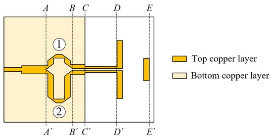
Figure 1.
Configuration of a quasi-Yagi antenna with a half-wave delay line splitter connected to a coplanar stripline.
Theoretically, between the two lines of DL at BB′, a balanced signal with a 180° phase difference is only obtained at the design frequency, probably at the center of the operating frequency. The two lines of the DL are not completely independent and may affect the phase balance of the two lines as a function of the DL gap width, but the interaction can be nonlinear [16]. However, the reported bandwidths of the quasi-Yagi antennas were not narrow but rather wide: the bandwidth was 3.4–6.3 GHz (60%) in [2], 8.9–14.8 GHz (50%) in [3], and 23.3–30.3 GHz (26%) in [4]. When the phase is not perfectly balanced at the antenna feed location, the radiated beam from the quasi-Yagi antenna will be steered at different oblique angles as a function of frequency.
A coplanar stripline (CPS) is attached at CC′, and a CPS is a balanced transmission line consisting of two uniplanar parallel lines [17,18]. The CPS is widely used in microwave circuits and often used as a balanced antenna feedline with a transition connected to an MSL. Various wideband MSL-to-CPS transition designs have been reported, including the smooth tapered lines or the resonant structures [19,20,21,22,23,24]. An improved performance of the quasi-Yagi antenna was reported using an ultra-wideband microstrip-to-CPS transition by the authors’ group [12].
Up to now, to the best of the authors’ knowledge, no clear description has been reported regarding how a half-wave delay line splitter connected to a CPS works as a wideband balun to feed a balanced antenna. In [12], the autonomous phase balancing effect of the CPS was briefly described, but the description was not in detail, i.e., a qualitative discussion without measurements. Recently, it has been reported by the authors’ group that the balanced lines have the ability of self-balancing the phase of differential signals in transmitting high-speed digital signals [16].
In this paper, the autonomous phase balancing action of the CPS as a balanced line is clearly demonstrated with the 3D EM simulations and measurements. For a demonstration, with the center frequency at 10 GHz, phase differences between the two signal lines of various half-wave delay line splitter structures connected to a CPS have been simulated and measured.
2. Feed Structure for Balanced Signals
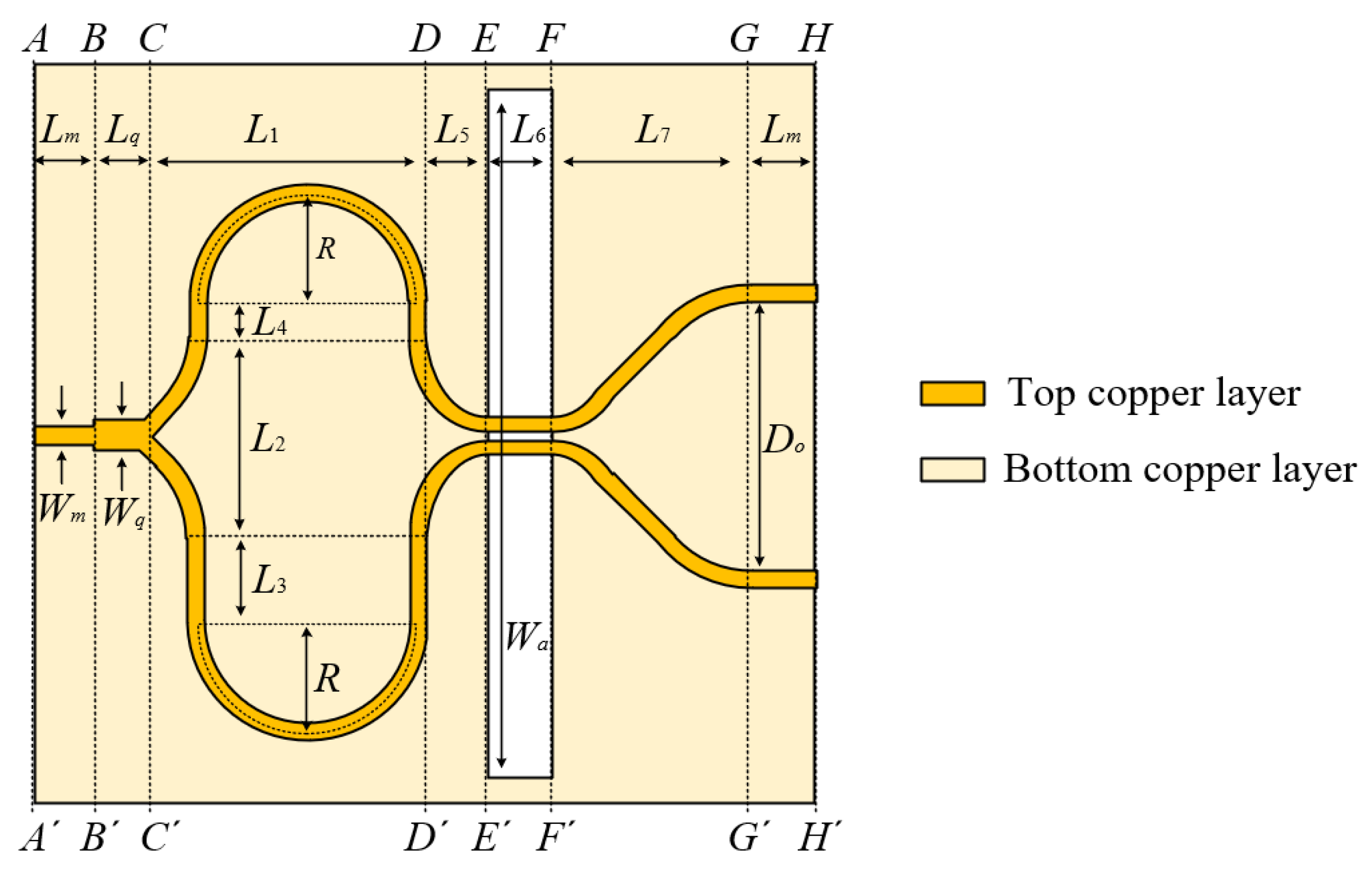
Figure 2 illustrates a model of a feed structure (BB′ to FF′) for a quasi-Yagi antenna with a half-wave delay line splitter structure. An additional section from FF′ to HH′ is added for the signal measurements with a 4-port network analyzer. The AA′–BB′ section is a 50 Ω MSL with linewidth Wm and length Lm. The MSL is split into two 50 Ω MSL paths, and the BB′–CC′ section is a quarter-wave transformer with linewidth Wq and length Lq for impedance matching between the input MSL and the two 50 Ω MSLs (CC′–DD′). In the CC′–DD′ section, the two MSLs are split in opposite directions, move away from each other, and then return to be located closely. The line section, L3, is longer than the other, L4, by a quarter wavelength at the selected frequency. Both MSLs have the linewidth of Wm and are curved with a radius of R to prevent EM coupling from the loops they create. In the DD′–EE′ section, the linewidth smoothly decreases while maintaining the differential impedance of 100 Ω, considering the EM interaction between the two lines as the gap distance becomes smaller.
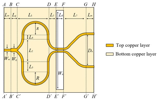
Figure 2.
Configuration of a half-wave delay line splitter connected to a coplanar stripline (or a differential line) with design parameters.
For the EE′–FF′ section, a CPS (or an extended DL), which feeds the quasi-Yagi antenna radiator strips, is shown. In order to monitor the phase balancing action of the feed line, this section has been configured with two types: (1) extending the 100 Ω DL with different linewidths and gaps and (2) connecting CPS lines with different linewidths. For the CPS lines, an aperture with width Wa exists at the bottom layer, while the DLs do not have a bottom aperture.
For the additional section from FF′ to HH′, which is added for the signal measurements, the two lines of the DL connected from the CPS (or the extended DL) move away from each other to smoothly form two 50 Ω MSLs with linewidth Wm. The design parameters of this structure are listed in Table 1. The center frequency of the structure is selected as 10 GHz for use as a balun structure for a quasi-Yagi antenna.

Table 1.
Design parameters of a half-wave delay line splitter with a CPS (or a DL).
3. Phase Balance of the Feed Structure
From the structure in Figure 2, the BB′–FF′ section is supposed to work as a balun, which transforms an unbalanced signal into a balanced one. For an ideal balun, the magnitudes of the two lines should be the same, and the phase difference between the two lines should be very close to 180° for the whole operating frequency range. For the EE′–FF′ section, two configurations are examined: (1) 100 Ω DLs with different linewidths and gaps and (2) CPS lines with different linewidths (124 Ω and 110 Ω).
For the quasi-Yagi antennas in the cited studies, the feedline gap was narrow and constant, and the feed linewidth was optimized for the antenna impedance matching [1,2,3,4,5,6,7,8,9,10,11,12,13,14]. In this paper, the gap between the two lines of a balanced antenna feed structure is set at 0.2 mm. On the Rogers RO4003C substrate (εr = 3.38, tanδ = 0.0027, 0.305 mm thickness), a 100 Ω DL can have a linewidth of 0.4 mm and a gap of 0.2 mm (DL0402). The connected CPS, with the same gap and linewidth (CPS0402), but with the ground removed from DL, has a characteristic impedance of 124 Ω. To lower the reflection level, the linewidth of the other CPS is set at 1.2 mm, with the 0.2 mm gap (CPS1202) having the characteristic impedance of 110 Ω. With the CPS, the lowest characteristic impedance is typically limited by the PCB fabrication constraints. With the other DL having a linewidth of 0.6 mm and a gap of 0.7 mm (DL0607), the two lines of the DL are sufficiently independent from the EM interactions due to a widely separated gap width of 0.7 mm. The DL0607 is chosen to show weak EM interactions between the two DL lines (as shown in Figure 3a). If a CPS with the same gap and linewidth is connected to DL0607, the characteristic impedance becomes 170 Ω, which is not suitable for this phase balancing analysis. In this case study, the phase balances and S-parameters are obtained via the 3D EM simulator (CST Microwave Studio).
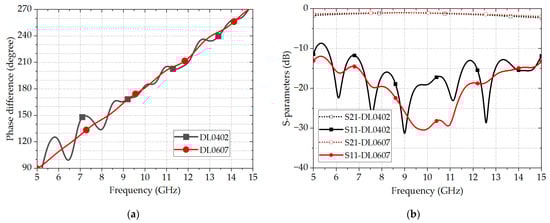
Figure 3.
Simulated results of DL0402 and DL0607: (a) phase differences between the two signal lines; (b) S-parameters of the back-to-back structures.
3.1. Phase Balance Test with DLs
The phase balances with two types of 100 Ω DLs with different linewidths and gaps (for the EE′–FF′ section in Figure 2) are compared, i.e., DL0402 and DL0607. The linewidth is indicated by the first two digits of each type name, and the gap is expressed by the final two digits, e.g., the DL0402 line has a linewidth of 0.4 mm and a gap of 0.2 mm. The rest of the structure is the same as shown in Figure 2.
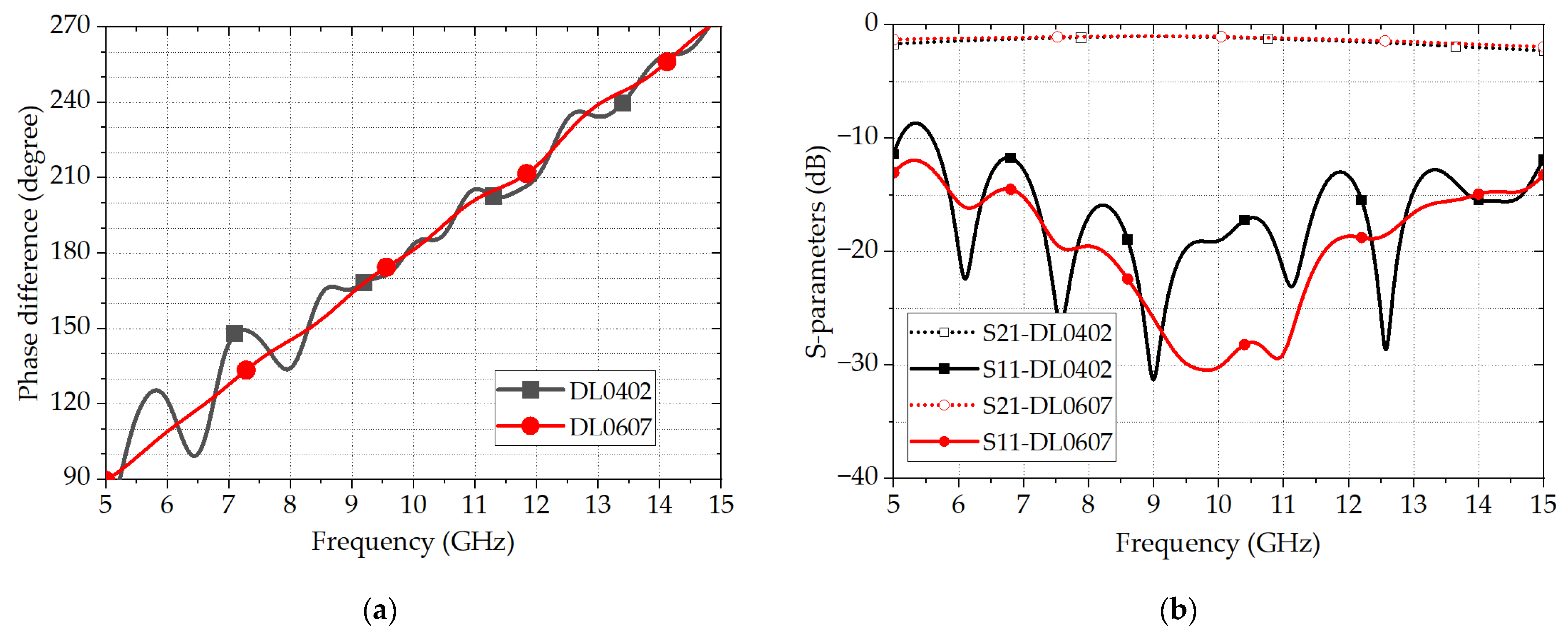
Figure 3a shows the phase differences between the two output signal lines with two different DL types. Since the center frequency (f0) of the structure is set at 10 GHz, the phase difference between the two output signal lines should be 180° at 10 GHz for the two types. As the frequency moves away from 10 GHz, the phase difference becomes proportionally deviated from the opposite polarity. Figure 3b shows the simulated S-parameters of the back-to-back structures, which consist of the section from AA′ to FF′ and then the section back to AA′, for both DL0402 and DL0607. From 5.6 to 15 GHz, the insertion loss per a single structure is less than 1.1 dB, and the return loss is greater than 10 dB for both cases. Of course, this structure cannot be used as a balun to feed a balanced antenna since the near 180° phase difference occurs at a very narrow frequency bandwidth around 10 GHz. In the figure, it is observed that the phase difference is almost linear with frequency (~π f/f0) when the gap between the two lines of a DL is wide (DL0607), but some phase nonlinearities occur with a narrow gap (DL0402). These phase imbalances, significantly deviating from the 180° phase difference, can cause the antenna beam to be incorrectly steered and may increase side-lobe levels, thereby reducing the antenna efficiency and potentially causing interference issues [25].
3.2. Phase Balance Test with CPS Lines
The phase balances with two types of CPS lines with different linewidths (for the EE′–FF′ section in Figure 2) are compared, i.e., CPS0402 and CPS1202. Once again, the linewidth is indicated by the first two digits of each type name, and the gap is expressed by the final two digits. The two signal lines of the CPS are subsequently connected to two microstrip lines (FF′ to HH′ section in Figure 2) for the measurements.
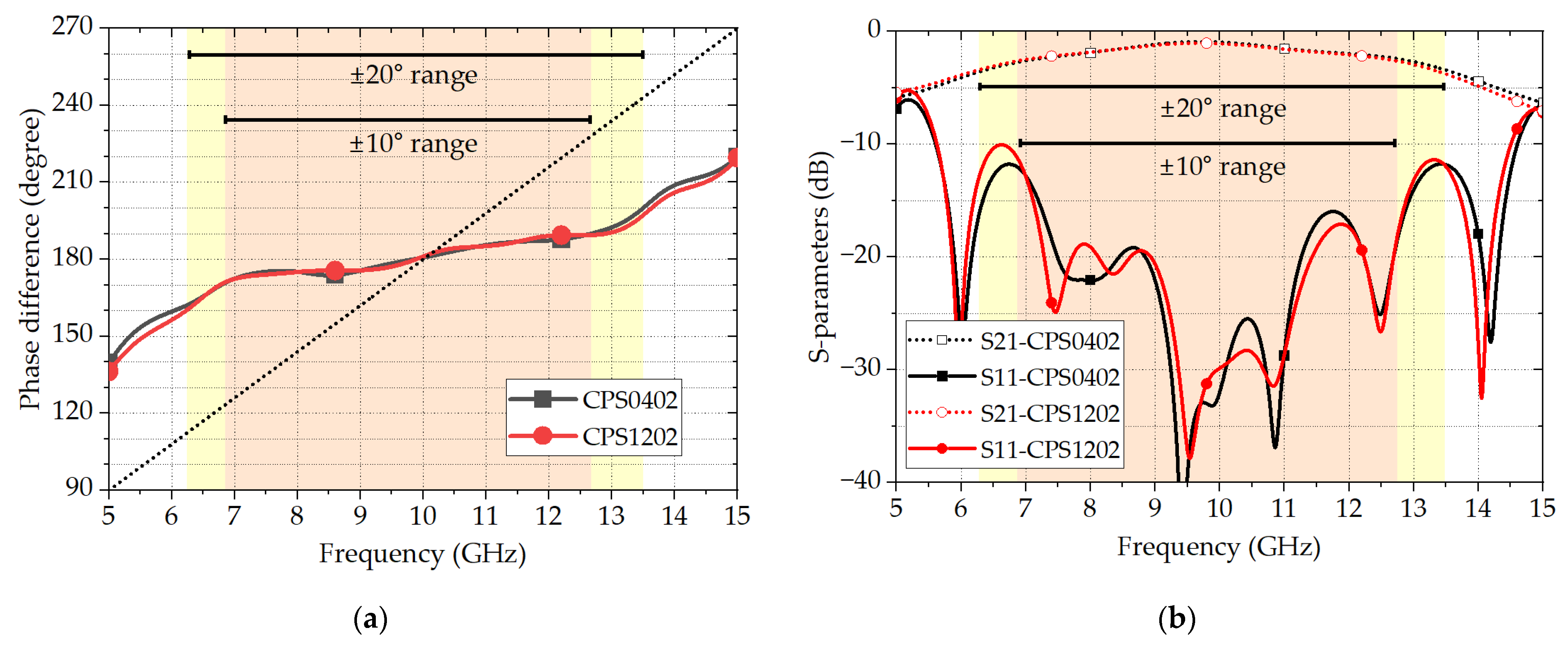
Figure 4a shows the phase differences between two output lines of two CPS types. In these cases, it can be observed that the phase difference values behave quite differently from those of DLs placed in the EE′–FF′ section (Figure 3). For both CPS types, the phase differences are maintained close to 180° within a range of ±20° from 6.2 to 13.5 GHz, as well as within a range of ±10° from 6.8 to 12.7 GHz. Below 6.2 GHz and beyond 13.5 GHz, the phase differences between incoming signals from the half-wave splitter are too big (>π/3) for the CPS to recover the phase balance of the two lines to maintain the opposite polarity. Additionally, Figure 4b shows the simulated S-parameters of the back-to-back structures, which consist of the section from AA’ to FF’, and then the section back to AA′, for both CPS0402 and CPS1202. From 5.6 to 14.5 GHz, the return loss is greater than 10 dB in both cases. The insertion loss per a single structure is less than 1.9 dB in the frequency range of 6.2 to 13.5 GHz and less than 1.3 dB in the frequency range of 6.8 to 12.7 GHz. Consequently, this structure, comprising a half-wave split path and a CPS, can be used as a balun with ~60% bandwidth (e.g., 6.8 to 12.7 GHz) to feed a wideband balanced antenna.
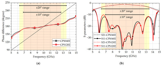
Figure 4.
Simulated results of CPS0402 and CPS1202: (a) phase differences between the two signal lines; (b) S-parameters of the back-to-back structures.
Therefore, this type of balun structure can be conveniently utilized as a balanced feedline for an antenna with less than ~60% bandwidth, but it cannot be used for antennas with wider bandwidth. All of the reported quasi-Yagi antennas with this type of feeding structure had a frequency bandwidth of less than ~60% [1,2,3,4,5,6,7,8].
4. Fabrication and Measurement
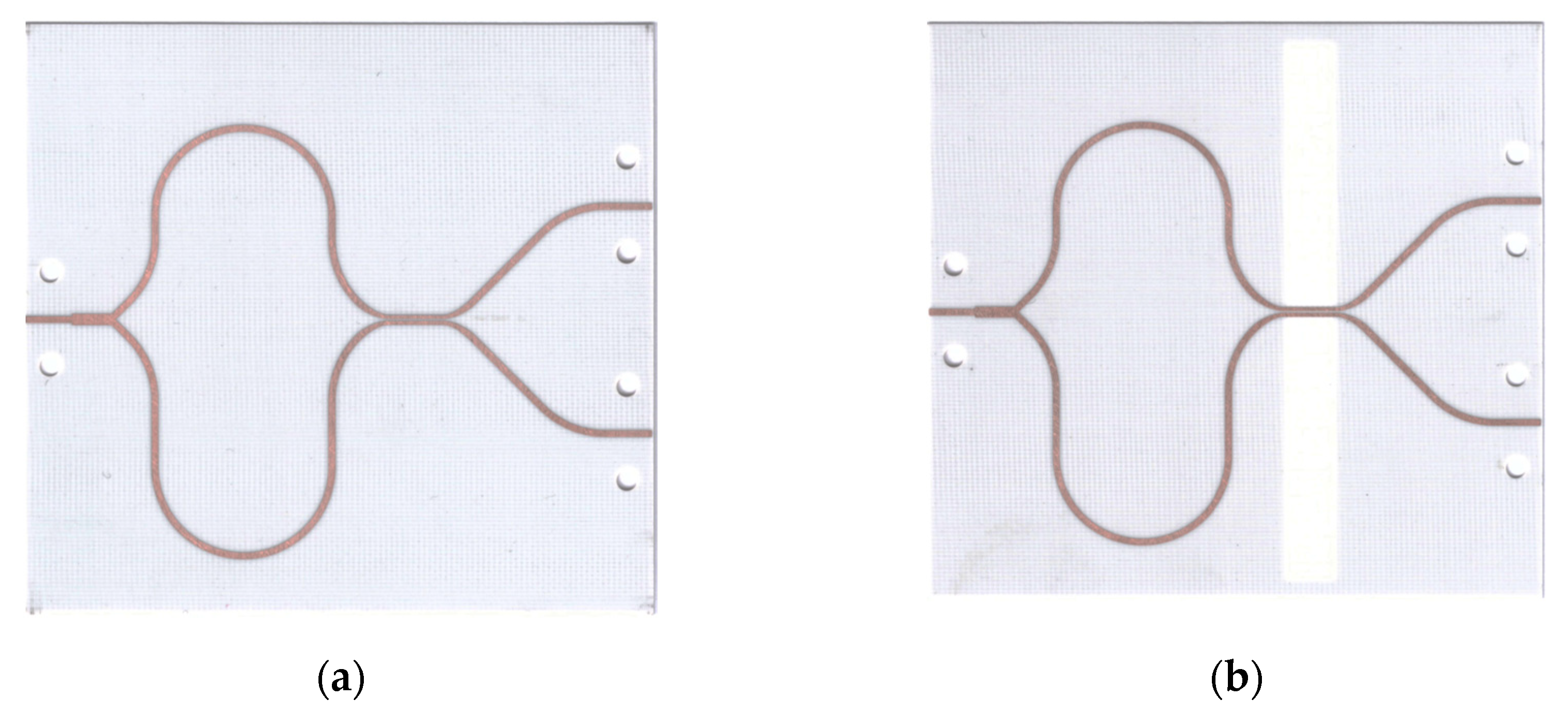
To verify the phase balance of the antenna feed structures (shown in Figure 2) with measurements, two types of the sample structures are fabricated: DL0402 and CPS0402. These half-wave delay line splitter samples are fabricated on the Rogers RO4003C substrate (εr = 3.38, tanδ = 0.0027, 0.305 mm thickness), and their overall sizes are 64.1 mm × 60.0 mm, as shown in Figure 5. Each structure, consisting of one MSL input and two MSL output ports, is measured via a 4-port network analyzer (Rohde and Schwarz ZNB40, Germany).
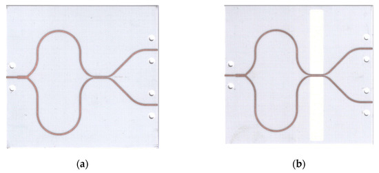
Figure 5.
Fabricated half-wave delay line splitter samples: (a) DL0402; (b) CPS0402.
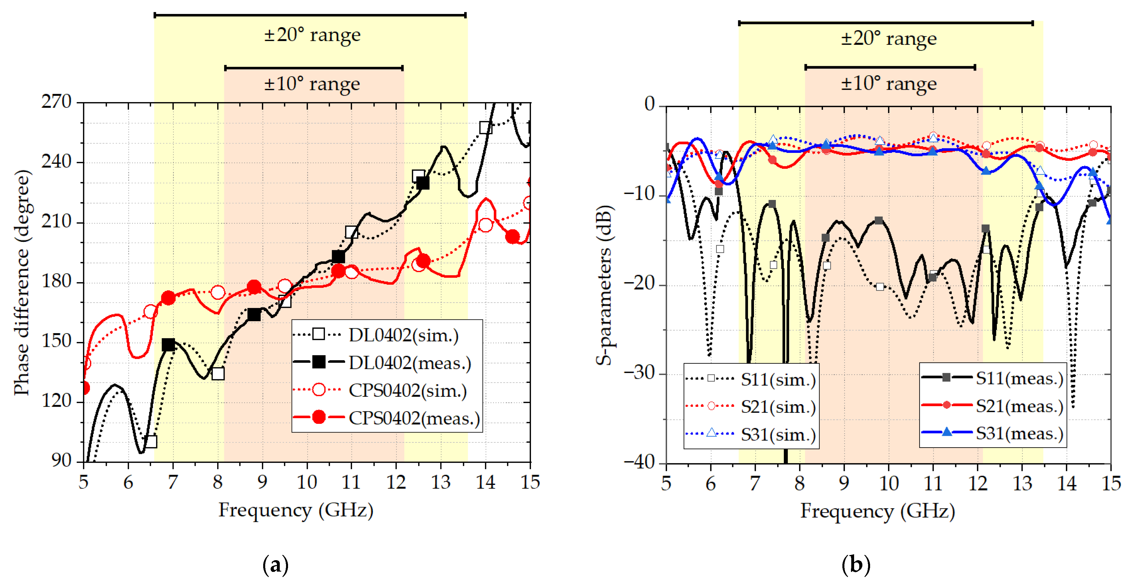
The measured phase differences of the two samples with simulated results are compared in Figure 6a. With the half-wave delay line splitter connected to the DL line, the phase imbalance occurs at up to ±60° for the frequency range of 6.5 to 12.8 GHz. On the other hand, with the half-wave delay line splitter connected to the CPS, the phase differences are maintained close to 180° within a range of ±20° from 6.6 to 13.5 GHz, as well as within a range of ±10° from 8.2 to 12.2 GHz. While the measured results agree with the simulated ones on the whole, the measured phase difference values show some resonant fluctuations over the frequencies, and the frequency range of ±10° phase balance is somewhat reduced compared to the simulated result. These resonances may have been caused by the loop structure (specifically, the CC′–EE′ section in Figure 2), and similar (or deeper) resonant behaviors were also observed in previous half-wave delay line splitter structures [5,12]. For this study, the size of the loop consisting of the two split MSL paths is set to be relatively large to mitigate the EM coupling and resonances.

Figure 6.
(a) Measured phase differences between the two output lines of the fabricated samples; (b) Measured S-parameters of the fabricated CPS0402.
These measurements clearly demonstrate that the CPS acts to regain the phase balance between two signal lines. It can be noted that the CPS can recover the phase balance between the signal lines if the phase difference is within ~π/3. If the phase difference is greater than ~π/3, the CPS may have a limitation to fully recover the phase balance.
Figure 6b shows amplitude balances (S21 and S31) and return losses (|S11|) for CPS0402. In the frequency range of 8.2 to 12.2 GHz, as a phase balance range of ±10°, the maximum amplitude difference between the output signals is 2.0 dB, while the average amplitude difference is 0.5 dB. The return loss bandwidth (>10 dB) is very wide (from 6.6 to 13.5 GHz), but the amplitude difference can reach up to 5.3 dB. Therefore, it can be noted that the frequency bandwidth based on the return loss alone may not be an accurate indication of the phase balance bandwidth.
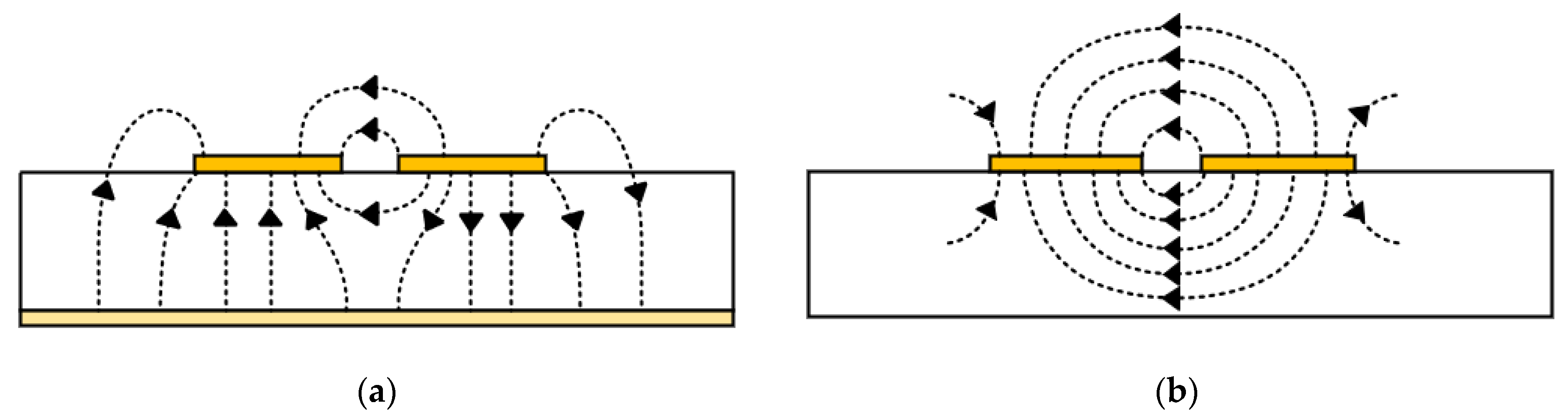
Figure 7a,b show electric field line distributions for a DL and a CPS. With the DL, most of the field lines are concentrated between each signal line and the ground plane, and some portion of the field lines is coupled between the lines. These coupled field lines may interact to change the phase imbalance, but they mostly result in an incomplete and nonlinear phase balance. With the CPS, most of the field lines are contained between the two signal lines, and, thus, the two lines are strongly coupled. This strong EM interaction enables us to recover the phase balance between the two signal lines of CPS when a differential signal with a phase imbalance propagates into the CPS.
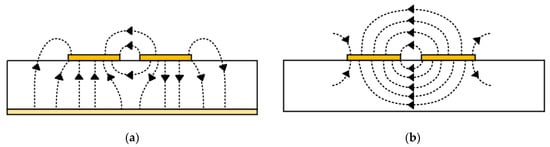
Figure 7.
Electric field line distributions: (a) DL; (b) CPS.
Therefore, by utilizing this autonomous phase balancing action of the balanced lines (e.g., a CPS and a parallel stripline), a simple balun structure can be formed with a half-wave delay line splitter connected to a balanced line. This type of balun structure can be very useful for frequency bandwidths within ~60%.
5. Conclusions
In this paper, an autonomous phase balancing action of a CPS in the presence of a phase imbalance between two input signal lines to the CPS has been clearly described via 3D EM simulations and measurements. This experiment explains how a half-wave delay line splitter connected to a CPS works as a broadband balun to feed balanced antennas, such as a quasi-Yagi antenna. The half-wave delay line splitter alone provides a 180° phase difference at only one frequency, but the connected CPS acts to restore the phase balance between the two signal lines if the input phase difference is within ~±π/3, which determines the bandwidth of the structure as a balun. For a demonstration, two samples of the half-wave delay line splitter, connected to a DL or a CPS at the design frequency of 10 GHz, were designed and fabricated. The phase and amplitude differences of the samples were measured as a function of frequency and compared to the 3D EM simulations. These results justify using the half-wave delay line splitter connected to a balanced line as a broadband balun to feed balanced antennas or components.
Author Contributions
Conceptualization, J.-S.L., B.-C.M. and K.-W.K.; methodology, J.-S.L. and B.-C.M.; software, J.-S.L.; validation, J.-S.L., B.-C.M., H.-C.C. and K.-W.K.; formal analysis, J.-S.L. and B.-C.M.; investigation, J.-S.L. and B.-C.M.; resources, J.-S.L. and B.-C.M.; data curation, J.-S.L., B.-C.M. and S.K.; writing—original draft preparation, J.-S.L. and K.-W.K.; writing—review and editing, B.-C.M., H.-C.C. and K.-W.K.; visualization, J.-S.L. and B.-C.M.; supervision, H.-C.C. and K.-W.K.; project administration, K.-W.K.; funding acquisition, K.-W.K. All authors have read and agreed to the published version of the manuscript.
Funding
This research was supported in part by the BK21 FOUR project funded by the Ministry of Education (No. 4199990113966) and in part by the Korean Government (MSIT) (No. EN2301-1).
Data Availability Statement
Not applicable.
Conflicts of Interest
The authors declare no conflict of interest.
References
- Qian, Y.; Deal, W.R.; Kaneda, N.; Itoh, T. Microstrip-fed quasi-Yagi antenna with broadband characteristics. Electron. Lett. 1998, 34, 2194–2196. [Google Scholar]
- Qian, Y.; Deal, W.R.; Sor, J.; Itoh, T. A novel printed antenna with broadband circular polarization. In Proceedings of the 1999 Asia Pacific Microwave Conference, Singapore, 30 November–3 December 1999; Volume 1, pp. 142–145. [Google Scholar]
- Song, H.J.; Bialkowski, M.E. Investigations into the operation ob a microstrip-fed uniplanar quasi-Yagi antenna. In Proceedings of the IEEE Antennas and Propagation Society International Symposium, Salt Lake City, UT, USA, 16–21 July 2000; Volume 3, pp. 1436–1439. [Google Scholar]
- Satyanarayana, B.; Vadlamudi, R.; Meshram, M.K. A Wideband Quasi-Yagi Antenna Array at 24–28 GHz for 5G mmWave Mobile Terminals. In Proceedings of the 2022 IEEE Microwaves, Antennas, and Propagation Conference (MAPCON), Bangalore, India, 12–16 December 2022; pp. 1546–1550. [Google Scholar]
- Deal, W.R.; Kaneda, N.; Sor, J.; Qian, Y.; Itoh, T. A new quasi-Yagi antenna for planar active antenna arrays. IEEE Trans. Microw. Theory Tech. 2000, 48, 910–918. [Google Scholar] [CrossRef]
- Eldek, A.A.; Elsherbeni, A.Z.; Smith, C.E. Microstrip-fed printed lotus antenna for wideband wireless communication systems. IEEE Antennas Propag. Mag. 2004, 46, 164–173. [Google Scholar] [CrossRef]
- Sun, Y.; Zhang, H.; Wen, G.; Wang, P. Research Progress in Yagi Antennas. Procedia Eng. 2012, 29, 2116–2121. [Google Scholar] [CrossRef]
- Silva, I.B.T.; Silva, S.G.; Silva, M.F.D.; Andrade, H. Quasi-Yagi microstrip antenna device design for directive wideband ISM application. Microw. Opt. Technol. Lett. 2017, 59, 3042–3046. [Google Scholar] [CrossRef]
- Kan, H.K.; Waterhouse, R.B.; Abbosh, A.M.; Bialkowski, M.E. Simple Broadband Planar CPW-Fed Quasi-Yagi Antenna. IEEE Antennas Wirel. Propag. Lett. 2007, 6, 18–20. [Google Scholar] [CrossRef]
- Ma, T.G.; Wang, C.W.; Hua, R.C.; Tsai, J.-W. A Modified Quasi-Yagi Antenna With a New Compact Microstrip-to-Coplanar Strip Transition Using Artificial Transmission Lines. IEEE Trans. Antennas Propag. 2009, 57, 2469–2474. [Google Scholar]
- Ta, S.X.; Kim, B.; Choo, H.; Park, I. Wideband quasi-yagi antenna fed by microstrip-to-slotline transition. Microw. Opt. Technol. Lett. 2012, 54, 150–153. [Google Scholar] [CrossRef]
- Woo, D.S.; Cho, Y.K.; Kim, K.W. Balance Analysis of Microstrip-to-CPS Baluns and Its Effects on Broadband Antenna Performance. Int. J. Antennas Propag. 2013, 2013, 651040. [Google Scholar]
- Elsheakh, D.M.; Abdallah, E.A. Ultra wide band planar printed quasi-Yagi antenna with size reduction for water detection in the Egyptian desert. Microw. Opt. Technol. Lett. 2015, 57, 226–233. [Google Scholar]
- Aeini, M.; Jarchi, S.; Faraji-Dana, R. Compact, wideband-printed quasi-Yagi antenna using spiral metamaterial resonators. Electron. Lett. 2017, 53, 1393–1394. [Google Scholar] [CrossRef]
- Hall, S.H.; Heck, H.L. Advanced Signal Integrity for High-Speed Digital Design; John Wiley & Sons: New York, NY, USA, 2009; pp. 297–314. [Google Scholar]
- Min, B.C.; Lee, G.H.; Lee, J.S.; Nashuha, S.H.; Choi, H.C.; Kim, K.W. Ultra-Wideband Differential Line-to-Balanced Line Transitions for Super-High-Speed Digital Transmission. Sensors 2022, 22, 6873. [Google Scholar] [CrossRef] [PubMed]
- Knorr, J.B.; Kuchler, K. Analysis of Coupled Slots and Coplanar Strips on Dielectric Substrate. IEEE Trans. Microw. Theory Tech. 1975, 23, 541–548. [Google Scholar] [CrossRef]
- Goverdhanam, K.; Simons, R.N.; Katehi, L.P.B. Coplanar stripline propagation characteristics and bandpass filter. IEEE Microw. Guid. Wave Lett. 1997, 7, 214–216. [Google Scholar] [CrossRef]
- Suh, Y.H.; Chang, K. A wideband coplanar stripline to microstrip transition. IEEE Microw. Wirel. Compon. Lett. 2001, 11, 28–29. [Google Scholar] [CrossRef]
- Chiu, T.; Shen, Y.S. A broadband transition between microstrip and coplanar stripline. IEEE Microw. Wirel. Compon. Lett. 2003, 13, 66–68. [Google Scholar] [CrossRef]
- Tu, W.H.; Chang, K. Wide-band microstrip-to-coplanar stripline/slotline transitions. IEEE Trans. Microw. Theory Tech. 2006, 54, 1084–1089. [Google Scholar]
- Venkatesan, J. Novel Version of the Double-Y Balun: Microstrip to Coplanar Strip Transition. IEEE Antennas Wirel. Propag. Lett. 2006, 5, 172–174. [Google Scholar] [CrossRef]
- Lee, G.H.; Mohyuddin, W.; Choi, H.C.; Kim, K.W. Asymmetric ultra-wideband microstrip-to-coplanar stripline transition. IEEE Microw. Wirel. Compon. Lett. 2018, 28, 386–388. [Google Scholar] [CrossRef]
- Ouyang, Z.A.; Zhu, L.; Qiu, L.L. Wideband Balanced-to-Balanced Microstrip-to-Coplanar Strip Transitions With Intrinsic Common-Mode Suppression. IEEE Trans. Microw. Theory Tech. 2021, 69, 3726–3736. [Google Scholar] [CrossRef]
- Constantine, A.; Balanis. Antenna Theory: Analysis and Design, 3rd ed.; John Wiley & Sons: Hoboken, NJ, USA, 2016. [Google Scholar]

Disclaimer/Publisher’s Note: The statements, opinions and data contained in all publications are solely those of the individual author(s) and contributor(s) and not of MDPI and/or the editor(s). MDPI and/or the editor(s) disclaim responsibility for any injury to people or property resulting from any ideas, methods, instructions or products referred to in the content. |
© 2023 by the authors. Licensee MDPI, Basel, Switzerland. This article is an open access article distributed under the terms and conditions of the Creative Commons Attribution (CC BY) license (https://creativecommons.org/licenses/by/4.0/).