Abstract
In this study, we investigated the impact of intrinsic output conductance (goi) on the short-circuit current-gain cut-off frequency (fT) in InxGa1-xAs/In0.52Al0.48As quantum-well (QW) high-electron-mobility transistors. At its core, we attempted to extract values of fT using a simplified small-signal model (SSM) of the HEMTs and to derive an analytical formula for fT in terms of extrinsic model parameters that are related with intrinsic model parameters of a general SSM. We projected how fT was influenced by goi in HEMTs, emphasizing that the improvement in electrostatic integrity would also be of critical importance to fully benefit from scaling down Lg.
1. Introduction
The excellent carrier transport properties of InxGa1-xAs/In0.52Al0.48As material systems (x > 0.53) on an InP substrate, together with advances in material growth and device fabrication, have made InxGa1-xAs/In0.52A0.48As quantum-well (QW) HEMTs a strong candidate for high-frequency and terahertz (THz) system applications, as well as quantum computing applications [1,2,3,4,5,6,7,8,9,10,11,12,13,14,15,16]. Recent reports on the InxGa1-xAs/In0.52A0.48As QW HEMTs, with a fT value in excess of 700 GHz [17,18] and noise temperature of 2 K at cryogenic operation [19], have been published.
Until now, paths to improve the fT in HEMTs have involved reducing Lg down to below 30 nm, improving the mobility of two-dimensional electron gas (μn,2-DEG) in a QW channel, and minimizing all the parasitics such as series resistance and gate-fringing capacitance components [20,21,22,23,24,25,26,27,28,29,30,31].
In principle, the fT of a HEMT in saturation is a figure of merit that is widely benchmarked to evaluate the suitability of HEMTs for high-frequency analog, mixed-signal, and logic applications. Moreover, the physical meaning of fT is fundamentally indicative of electron transport through the intrinsic region of the QW channel. It is known that fT increases with the decrease in Lg due to the reduction in the electron transit time under the gate, while parasitic components hinder fT from linearly increasing with a reciprocal of Lg. Despite the fact that the impact of short-channel-effects (SCEs) on the logic characteristics of the HEMT has been extensively investigated [32,33], there have been few reports on how SCEs analytically affect the fT of a HEMT as Lg scales down to below 100 nm.
In this study, we extracted and analyzed values of the fT in In0.8Ga0.2As/In0.52A0.48As QW HEMTs on an InP substrate with Lg values ranging from 260 to 25 nm in three different manners: (i) a least-squares fit using experimental S-parameter data, (ii) a projection from both simplified and general small-signal models (SSMs), and (iii) a calculation from an analytical formula. These allowed us to systematically investigate how fT was affected by goi as Lg aggressively scales down in these devices.
2. Fabrication Process
Figure 1 provides a description of the heterostructure used for device fabrication in this study. All the epitaxial layers were grown by metal–organic chemical vapor deposition (MOCVD) on a 3-inch semi-insulating InP substrate with a crystal orientation of (100). A strained 5 nm thick In0.8Ga0.2As subchannel layer was incorporated to enhance the carrier transport properties in the QW channel, together with a 3 nm thick undoped InP layer as a gate recess etch stopper. It also featured a multilayer cap design to enhance the tunneling efficiency between the heavily doped capping layer and the In0.8Ga0.2As composite QW channel layer through an In0.52Al0.48As barrier layer in the source and drain access regions. The capping layer design consisted, from top to bottom, of a 12 nm thick heavily doped In0.53Ga0.47As subcapping layer with a Si doping concentration of 2 × 1019 cm−3 to lower the actual metal–semiconductor contact resistivity (ρc), and a 15 nm thick heavily doped In0.52Al0.48As subcapping layer with a Si doping concentration of 5 × 1018 cm−3 to lower the overall potential barrier across the In0.52Al0.48As barrier in the source and drain access regions. In a Hall epi wafer without the multilayer capping design, the Hall mobility (μn_hall) and two-dimensional electron gas density (n2-DEG) were measured to be around 13,500 cm2/V·s and 1.78 × 1012 cm−2 at room temperature, and 33,800 cm2/V·s and 1.74 × 1012 cm−2 at 77 K, respectively.
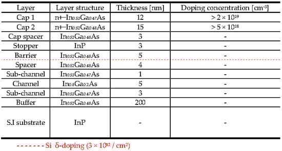
Figure 1.
The epitaxial layer structure of In0.8Ga0.2As/In0.52A0.48As composite-channel QW HEMTs fabricated in this work.
The device fabrication was comparable in detail to that we previously reported [34]. It involved a two-step recess process with a gate-to-channel distance (tins) of approximately 5 nm, as shown in Figure 2. The process began with device isolation by means of mesa etching using a dilute H3PO4-based wet-etching solution. Source-to-drain spacing (LSD) was scaled down to 1 μm, and a nonalloyed metal stack of Ti/Mo/Ti/Pt/Au (5/10/10/10/25 nm) was used to form S/D ohmic contacts. Here, we intentionally thinned the S/D ohmic metals to 60 nm to obtain a uniform coating of the first ZEP e-beam resist in a trilayer e-beam resist scheme during T-gate e-beam lithography. From transmission-line method (TLM) analysis, an extremely low ohmic contact resistivity (ρc) of 9.4 × 10⁻⁸ Ω cm2 and an excellent standard deviation (σ) of 9.9 × 10⁻⁹ Ω cm2 across a 3 inch wafer were obtained. After contact pad formation of Ti/Au (20/500 nm), a 20 nm thick SiO2 was created between the source and drain ohmic contacts by plasma-enhanced chemical vapor deposition (PECVD). After a gate recess process, a SiO2-assisted T-gate with a metal stack of Pt/Ti/Pt/Au was created using a JBX-9300FS e-beam lithography machine operating at 100 kV, with the T gate placed in a tightly spaced source and a drain with less than 50 nm alignment accuracy. In this way, devices with three different Lg values of 260, 87, and 25 nm, were fabricated.
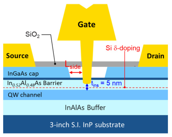
Figure 2.
A schematic of the In0.8Ga0.2As/In0.52Al0.48As QW HEMT in this study.
3. Theoretical Analysis of fT
fT in an HEMT is defined as a frequency such that its short-circuit current gain (h21(f)) becomes a unity. This is mathematically given as
Historically, fT was extracted by using a least-squares fit of |h21(f)|2 with a slope of −20 dB/decade, which was transformed from the measured S-parameter data. In parallel, small-signal equivalent circuit models of HEMTs have been constructed to describe the high-frequency characteristics not only within but also beyond the measured frequency ranges. Figure 3a represents the most widely used general SSM of HEMTs. According to the previous report by Tasker and Hughes [35], a 1st-order analytical formula for fT was derived as
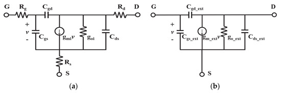
Figure 3.
(a) General small-signal model and (b) simplified small-signal model for an In0.8Ga0.2As/In0.52Al0.48As QW HEMT.
Using the equation above, many researchers have carried out delay time analysis [7,36,37,38,39,40], where the total delay (τ) of the HEMT consists of three terms: the intrinsic delay (τt), the delay through Cgd associated with the Miller effect (τext), and the parasitic delay due to the series resistances of Rs and Rd (τpar). Mathematically, the total delay and three delay terms are given as follows:
In most cases, the right-hand side (RHS) of Equation (6) is simplified as τpar ~ Cgd (Rs + Rd), because the open-circuit voltage gain (gmi/goi) was sufficiently large. As a result, this delay has been interpreted as the delay due to the parasitic series resistances of Rs and Rd. However, as Lg aggressively scales down, this is no longer true, and the impact of goi should be carefully considered. Moreover, it would be imperative to accurately extract the values of Rs and Rd; otherwise, this would affect not only other small-signal model parameters but also the delay terms even with the same fT value.
Alternatively, a simplified SSM of the HEMT is shown in Figure 3b, where all the model parameters, such as gm_ext, go_ext, Cgs_ext, Cgd_ext, and Cds_ext, include the effects of the series resistance components (Rg, Rs, and Rd). As in [41,42], all the model parameters in Figure 3a,b could be extracted analytically from the measured S-parameter data. Table 1 shows the modeled parameters of both general and simplified SSMs for In0.8Ga0.2As/In0.52Al0.48As QW HEMTs on InP substrate with Lg = 260, 87, and 25 nm [18]. Using the definition above, an analytical formula for the fT of Figure 3b is expressed as

Table 1.
Modeled parameters of both general and simplified small-signal models (SSMs) for In0.8Ga0.2As/In0.52Al0.48As QW HEMTs with Lg = 260/87/25 nm, Wg = 2 20 μm, and Rs/Rd/Rg = 3.8/3.8/6 Ω.
Figure 4a plots three different types of short-circuit current gain against the measured frequency together with the least-squares fits with a slope of −20 dB/decade: (i) measured |h21(f)|2, (ii) simulated |h21(f)|2 from Figure 3a, and (iii) simulated |h21(f)|2 from Figure 3b. Figure 4b plots the locally extrapolated fT at each frequency with a slope of −20 dB/decade. Note that both small-signal modeled current gains are in excellent agreement with the measured one, and their projected values of fT are consistent with those from the analytical formula in Equation (7). Table 2 summarizes the fT values using the different approaches explained above, indicating that the simplified SSM provides a fairly accurate value of fT in a HEMT. In comparison with the approach using Equation (2), the approach proposed in this paper does not need to accurately extract values of Rs and Rd. Instead, the simplified SSM, which is from the extrinsic perspective of the equivalent circuit, can be robustly constructed directly from the measured small-signal S parameters of the device, where fT can be analytically and uniquely given by Equation (7). To see how the intrinsic output conductance (goi) affects the fT of short-Lg HEMTs, we derived analytical expressions for gm_ext, Cgs_ext, and Cgd_ext in terms of the model parameters of the general SSM (Figure 3a). In the course of correlating admittance parameters between the general and simplified SSMs, Kirchhoff’s voltage and current laws, respectively, yield
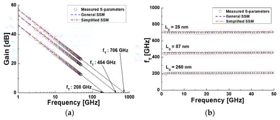
Figure 4.
(a) Three different types of the short-circuit current gain against the measured frequency together with least squares fits with a slope of −20 dB/decade, and (b) locally extrapolated fT at a given frequency for the same family of devices.
Table 2.
Values of fT extracted in different manners for the same family of In0.8Ga0.2As/In0.52Al0.48As QW HEMTs with Lg = 260/87/25 nm.
Here, we made two approximations: (i) ignorance of the 2nd-order of the frequency terms (ω2), and (ii) ignoring the effect of τ. This makes sense because the effects of both were negligible in the measured frequency ranges from 1 to 50 GHz. Interestingly, all the three equations contain the same form of the denominator, including the terms of gmi × Rs and goi × (Rs + Rd). Both make the extrinsic model parameters apart from the intrinsic model parameters. Plugging the results obtained in Equations (8)–(10) to Equation (7), we can derive Equation (2) and obtain a complete picture how fT evolves with goi in an HEMT.
4. Results and Discussion
We now look into the impact of short-channel effects (SCEs) on fT. To do so, we arbitrarily varied values of the intrinsic output conductance in Figure 3a for the devices with three different values of Lg, reconstructed new sets of the general SSM for each intrinsic output conductance, and extracted values of gm_ext, Cgs_ext, Cgd_ext, and fT using the approaches explained in Equations (8)–(10). Figure 5a–c plot gm_ext, Cgs_ext, and Cgd_ext, respectively, as a function of the intrinsic output conductance for the same family of devices. Symbols correspond to those from the small-signal modeling with the measured intrinsic output conductance for each device, whereas lines correspond to the projected ones that come from Equations (8)–(10) with different values of the intrinsic output conductance. First, Cgs_ext was nearly independent of goi. Because the ratio of Cgd/Cgs is typically much smaller than a unity, the second term in the square bracket of numerator of Cgs_ext is approximated to goi × Rd, and Cgs_ext is denominated by the first term of the numerator in square brackets. It makes Cgs_ext independent of goi. In the case of gm_ext, the results in this study are broadly consistent with those from DC analysis [43]. gm_ext is increasingly degraded by goi as Lg scales down aggressively. Figure 6 shows the two terms of Cgd_ext for each Lg device. Looking at the second term in the square brackets (solid lines in Figure 6), it is no longer negligible and actually comparable to Cgd × (1+gmi Rs) at a goi of around 1 mS/μm. Overall, Cgd_ext increases with goi. It should be emphasized that the dependencies of gm_ext and Cgd_ext on goi, especially in short-Lg devices, are exactly where fT is deteriorated.
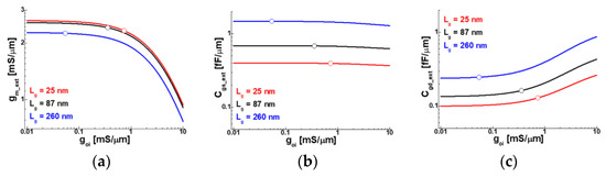
Figure 5.
(a) gm_ext, (b) Cgs_ext, and (c) Cgd_ext against goi for In0.8Ga0.2As/In0.52Al0.48As QW HEMTs with Lg from 260 to 25 nm.
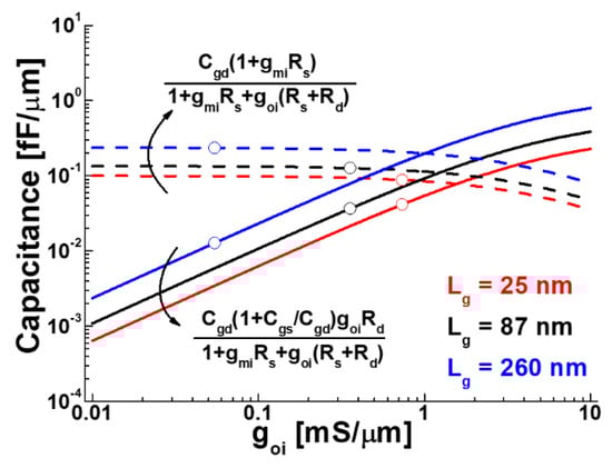
Figure 6.
Two terms of the numerator of Cgd_ext against goi for the In0.8Ga0.2As/In0.52Al0.48As QW HEMTs with Lg from 260 to 25 nm.
Next, we investigated how the degree of SCEs affects fT in detail. Figure 7 plots the projected fT for the devices with three different values of Lg, as a function of goi. Symbols correspond to the measured fT for each Lg device. The worse the SCEs, the more seriously fT degrades, which is the case for the device with Lg = 25 nm. For example, if improving a value of goi by a quarter for the device with Lg = 25 nm, it is projected that the fT would considerably improve from 706 to 802 GHz. Strikingly, this improvement would be comparable to or even surpass the benefit from scaling down Lg. This reveals that it would be of equal importance to pay close attention to the SCEs to maximize the improvement in the fT, in addition to the reduction in Lg and parasitic components, and the improvement in carrier transport properties in the InxGa1-xAs/In0.52Al0.48As QW channel layer. Unless goi is carefully engineered, indium-rich InxGa1-xAs/In0.52Al0.48As QW HEMTs with x > 0.53 and short Lg, which were originally incorporated to improve the high-frequency characteristics of the device, would be likely to deteriorate the electrostatic integrity of HEMTs and eventually be of no use in boosting fT.
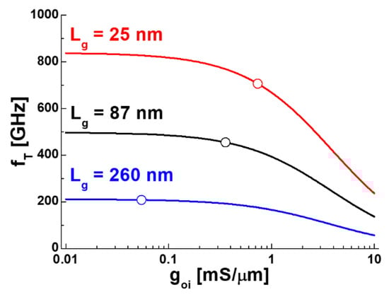
Figure 7.
Measured (symbols) and projected (lines) fT against goi for the In0.8Ga0.2As/In0.52Al0.48As QW HEMTs with Lg from 260 to 25 nm.
5. Conclusions
In summary, we investigated the impact of the electrostatic integrity of HEMTs on fT from the perspective of the simplified small-signal equivalent circuit. We extracted values of all the extrinsic model parameters and fT for In0.8Ga0.2As QW HEMTs with Lg = 260, 87, and 25 nm from the perspective of a simplified SSM, together with analytical expressions. In this way, we successfully explained the behavior of fT in those devices with respect to electrostatic integrity. As Lg considerably scaled down, we found that the degradation of the fT become more prominent. This is because the increase in the intrinsic output conductance caused the increase in the total extrinsic gate capacitance and the decrease in the extrinsic transconductance, leading to the degradation of fT. The results of this study indicate that it will be of great importance to pay close attention to SCEs to obtain a maximum improvement in fT in short Lg HEMTs.
Author Contributions
Conceptualization, H.-J.K., T.-W.K. and D.-H.K.; device fabrication, H.-J.K., I.-G.L., H.-B.J. and D.-H.K.; formal analysis, H.-J.K., T.T., H.S., H.M. and D.-H.K.; investigation, H.-J.K., T.-B.R., J.-H.L. and D.-H.K.; resources, H.-J.K., J.-H.L., T.-W.K. and D.-H.K.; writing—original draft preparation, H.-J.K. and T.-B.R.; writing—review and editing, I.-G.L. and H.-B.J.; supervision, J.-H.L., T.-W.K. and D.-H.K.; funding acquisition, T.-W.K. and D.-H.K. All authors have read and agreed to the published version of the manuscript.
Funding
This research was supported by the Civil-Military Technology Cooperation program (No. 19-CM-BD-05).
Data Availability Statement
The data presented in this study are available on request from the corresponding author.
Acknowledgments
This work was supported by Institute for Information & Communications Technology Planning & Evaluation (IITP) grant funded by the Korea government(MSIP) (No. 2020-0-00459).
Conflicts of Interest
The authors declare no conflict of interest.
References
- Hornibrook, J.M.; Colless, J.I.; Lamb, I.D.C.; Pauka, S.J.; Lu, H.; Gossard, A.C.; Watson, J.D.; Gardner, G.C.; Fallahi, S.; Manfra, M.J.; et al. Cryogenic Control Architecutre for Large-Scale Quantum Computing. Phys. Rev. Appl. 2015, 3, 024010. [Google Scholar] [CrossRef]
- Leong, K.M.H.; Mei, X.; Yoshida, W.H.; Zamora, A.; Padilla, J.G.; Gorospe, B.S.; Nguyen, K.; Deal, W.R. 850 GHz receiver and transmitter front-end using InP HEMT. IEEE Trans. Terahertz Sci. Technol. 2017, 7, 466. [Google Scholar] [CrossRef]
- Deal, W.R.; Leong, K.; Zamora, A.; Gorospe, B.; Nguyen, K.; Mei, X.B. A 660 GHz up-converter for THz communications. In Proceedings of the IEEE Compound Semiconductor Integrated Circuit Symposium (CSICS), Miami, FL, USA, 22–25 October 2017. [Google Scholar]
- Tessmann, A.; Leuther, A.; Wagner, S.; Massler, H.; Kuri, M.; Stulz, H.-P.; Zink, M.; Riessle, M.; Merkle, T. A 300 GHz low-noise amplifier S-MMIC for use in next-generation imaging and communication applications. In Proceedings of the IEEE MTT-S International Microwave Symposium (IMS), Honololu, HI, USA, 4–9 June 2017; p. 760. [Google Scholar]
- Ajayan, J.; Nirmal, D. A review of InP/InAlAs/InGaAs based transistors for high frequency applications. Superlattices Microstruc. 2015, 86, 1. [Google Scholar] [CrossRef]
- Rodwell, M.J.W.; Lee, S.; Huang, C.-Y.; Elias, D.; Chobpattanna, V.; Rode, J.; Chiang, H.-W.; Choudhary, P.; Maurer, R.; Urteaga, M.; et al. Nanometer InP electron devices for VLSI and THz applications. In Proceedings of the 72nd Annual Device Research Conference (DRC 2014), Santa Barbara, CA, USA, 22–25 June 2014; p. 215. [Google Scholar]
- Kim, D.-H.; Brar, B.; del Alamo, J.A. fT = 688 GHz and fmax = 800 GHz in Lg = 40 nm In0.7Ga0.3As MHEMTs with gm_max > 2.7 mS/µm. In Proceedings of the 2011 International Electron Devices Meeting, Washington, DC, USA, 5–7 December 2011; pp. 13.6.1–13.6.4. [Google Scholar]
- Kim, D.-H.; del Alamo, J.A. 30 nm InAs PHEMTs with ft=644 and fmax=681 GHz. IEEE Electron Device Lett. 2010, 31, 806. [Google Scholar]
- Kim, D.-H.; del Alamo, J.A. 30 nm E-mode InAs PHEMTs for THz and future logic application. IEEE Electron Device Lett. 2008, 29, 830. [Google Scholar] [CrossRef]
- Lai, R.; Mei, X.B.; Deal, W.R.; Yoshida, W.; Kim, Y.M.; Liu, P.H.; Lee, J.; Uyeda, J.; Radisic, V.; Lange, M.; et al. Sub 50 nm InP HEMT Device with fmax greater than 1 THz. In Proceedings of the 2007 IEEE International Electron Devices Meeting, Washington, DC, USA, 10–12 December 2007; pp. 609–611. [Google Scholar]
- Suemitsu, T.; Ishii, T.; Yokoyama, H.; Enoki, T.; Ishii, Y.; Tamamura, T. 30-nm-Gate InP-Based Lattice-Matched High Electron Mobility Transistors with 350 GHz Cutoff Frequency. Jpn. J. Appl. Phys. 1999, 38, 154. [Google Scholar] [CrossRef]
- Leuther, A.; Tessmann, A.; Dammann, M.; Massler, H.; Schlechtweg, M.; Ambacher, O. 35 nm mHEMT technology for THz and ultra low noise applications. In Proceedings of the 2013 International Conference on Indium Phosphide and Related Materials (IPRM), Kobe, Japan, 19–23 May 2013; pp. 1–2. [Google Scholar] [CrossRef]
- Kurita, Y.; Ducournau, G.; Coquillat, D.; Satou, A.; Kobayashi, K.; Boubanga Tombet, S.; Meziani, Y.M.; Popov, V.V.; Knap, W.; Suemitsu, T.; et al. Ultrahigh sensitive sub-terahertz detection by InP-based asymmetric dual-grating-gate high-electron-mobility transistors and their broadband characteristics. Appl. Phys. Lett. 2014, 104, 251114. [Google Scholar] [CrossRef]
- Radisic, V.; Leong, K.M.; Mei, X.; Sarkozy, S.; Yoshida, W.; Deal, W.R. Power amplification at 0.65 THz using INP HEMTs. IEEE Trans. Microw. Theory Tech. 2012, 60, 724. [Google Scholar] [CrossRef]
- Yeon, S.-J.; Par, M.-H.; Choi, J.; Seo, K.-S. 610 GHz InAlAs/In0.75Ga0.25As Metamorphic HEMTs with an Ultra-Short 15-nm-Gate. In Proceedings of the 2007 IEEE International Electron Devices Meeting, Washington, DC, USA, 10–12 December 2007; pp. 613–616. [Google Scholar]
- Watanabe, T.; Boubanga-Tombet, S.A.; Tanimoto, Y.; Fateev, D.; Popov, V.; Coquillat, D.; Knap, W.; Meziani, Y.M.; Wang, Y.; Minamide, H.; et al. InP- and GaAs-Based Plasmonic High-Electron-Mobility Transistors for Room-Temperature Ultrahigh-Sensitive Terahertz Sensing and Imaging. IEEE Sens. J. 2013, 13, 89–99. [Google Scholar] [CrossRef]
- Chang, E.-Y.; Kuo, C.-I.; Hsu, H.-T.; Chiang, C.-Y.; Miyamoto, Y. InAs Thin-Channel High-Electron-Mobility Transistors with Very High Current-Gain Cutoff Frequency for Emerging Submillimeter-Wave Applications. Appl. Phys. Exp. 2013, 6, 034001. [Google Scholar] [CrossRef]
- Jo, H.-B.; Yun, D.-Y.; Baek, J.-M.; Lee, J.-H.; Kim, T.-W.; Kim, D.-H.; Tsutsumi, T.; Sugiyama, H.; Matsuzaki, H. Lg = 25 nm InGaAs/InAlAs high-electron mobility transistors with both fT and fmax in excess of 700 GHz. Appl. Phys. Exp. 2019, 12, 054006. [Google Scholar] [CrossRef]
- Rodrigues, I.H.; Niepce, D.; Pourkabirian, A.; Moschetti, G.; Schleeh, J.; Bauch, T.; Grahn, J. On the angular dependence of InP high electron mobility transistors for cryogenic low noise amplifiers in a magnetic field. AIP Adv. 2019, 9, 085004. [Google Scholar] [CrossRef]
- Takahashi, T.; Kawano, Y.; Makiyama, K.; Shiba, S.; Sato, M.; Nakasha, Y.; Hara, N. vEnhancement of fmax to 910 GHz by adopting asymmetric gate recess and double-side-doped structure in 75-nm-gate InAlAs/InGaAs HEMTs. IEEE Trans. Electron Devices 2017, 64, 89. [Google Scholar] [CrossRef]
- Sugiyama, H.; Hoshi, T.; Yokoyama, H.; Matsuzaki, H. Metal-organic vapor-phase epitaxy growth of InP-based HEMT structures with InGaAs/InAs composite channel. In Proceedings of the 2012 International Conference on Indium Phosphide and Related Materials, Santa Barbara, CA, USA, 27–30 August 2012; pp. 245–248. [Google Scholar]
- Yun, D.-Y.; Jo, H.-B.; Son, S.-W.; Baek, J.-M.; Lee, J.-H.; Kim, T.-W.; Kim, D.-H.; Tsutsumi, T.; Sugiyama, H.; Matsuzaki, H. Impact of the source-to-drain spacing on the DC and RF characteristics of InGaAs/InAlAs high-electron mobility transistors. IEEE Electron Device Lett. 2018, 39, 1844. [Google Scholar] [CrossRef]
- Ajayan, J.; Nirmal, D. 20 nm high performance enhancement mode InP HEMT with heavily doped S/D regions for future THz applications. Superlattices Microstruc. 2016, 100, 526. [Google Scholar] [CrossRef]
- Li, Z.; An, N.; Zeng, J.; Tong, X.; Wang, W.; Li, Q.; Liu, H.; Liang, Y.; Tang, H.; Xiong, Y.-Z. Studying on source/drain contact resistance reduction for InP-based HEMT. Microw. Opt. Technol. Lett. 2016, 58, 217. [Google Scholar] [CrossRef]
- Takahashi, T.; Makiyama, K.; Hara, N.; Sato, M.; Hirose, T. Improvement in high frequency and noise characteristics of InP based HEMTs by reducing parasitic capacitance. In Proceedings of the 2008 20th International Conference on Indium Phosphide and Related Materials, Versailles, France, 25–29 May 2008; pp. 1–4. [Google Scholar]
- Shinohara, K.; Tamashita, Y.; Endoh, A.; Watanabe, I.; Hikosaka, K.; Matsui, T.; Mimura, T.; Hiyamizu, S. 547-GHz ft In 0.7Ga0.3As-In0.52Al0.48As HEMTs with reduced source and drain resistance. IEEE Electron Device Lett. 2004, 25, 241. [Google Scholar] [CrossRef]
- Shinohara, K.; Yamashita, Y.; Endoh, A.; Watanabe, I.; Hikosaka, K.; Mimura, T.; Hiyamizu, S.; Matsui, T. “550 GHz- pseudomorphic InP-HEMTs with reduced source/drain resistance. In Proceedings of the 61st Device Research Conference. Conference Digest, Salt Lake City, UT, USA, 23–25 June 2003; pp. 145–146. [Google Scholar]
- Makiyama, K.; Takahashi, T.; Suzuki, T.; Sawada, K.; Ohki, T.; Nishi, M.; Hara, N.; Takikawa, M. Improvement of circuit-speed of HEMTs IC by reducing the parasitic capacitance. In Proceedings of the IEEE International Electron Devices Meeting 2003, Washington, DC, USA, 8–10 December 2003; pp. 30–36. [Google Scholar]
- Yue, Y.; Hu, Z.; Guo, H.; Sensale-Rodiriguez, B.; Li, G.; Wang, R.; Faria, F.; Fang, T.; Song, B.; Gao, X.; et al. InAlN/AlN/GaN HEMTs With Regrown Ohmic Contacts and fT of 370 GHz. IEEE Electron Device Lett. 2012, 33, 988. [Google Scholar] [CrossRef]
- Shinohara, K.; Corrion, A.; Regan, D.; Milosavljevic, I.; Brown, D.; Burnham, S.; Willadsen, P.J.; Butler, C.; Schmitz, A.; Wheeler, D.; et al. 220GHz fT and 400GHz fmax in 40-nm GaN DH-HEMTs with re-grown ohmic. In Proceedings of the 2010 International Electron Devices Meeting, San Francisco, CA, USA, 6–8 December 2010; pp. 30–31. [Google Scholar]
- Akagawa, K.; Fukuda, S.; Suemitsu, T.; Otsuji, T.; Yokohama, H.; Araki, G. Impact of T-gate electrode on gate capacitance in In0.7Ga0.3As HEMTs. Phys. Status Solidi C 2011, 8, 300. [Google Scholar] [CrossRef]
- Kim, D.-H.; del Alamo, A.; Lee, J.-H.; Seo, K.-S. Logic Suitability of 50-nm In0.7Ga0.3As HEMTs for Beyond-CMOS Applications. IEEE Trans. Electron Devices 2007, 54, 2606. [Google Scholar] [CrossRef]
- Chau, R.; Datta, S.; Doczy, M.; Doyle, B.; Jin, B.; Kavalieros, J.; Majumdar, A.; Metz, M.; Radosavljevic, M. Benchmarking nanotechnology for high-performance and low-power logic transistor applications. IEEE Trans. Nanotechnol. 2005, 4, 153. [Google Scholar] [CrossRef]
- Park, W.-S.; Jo, H.-B.; Kim, H.-J.; Choi, S.-M.; Yoo, J.-H.; Kim, J.-H.; Jeong, H.-S.; George, S.; Beak, J.-M.; Lee, I.-G.; et al. Sub-50 nm Terahertz In0.8Ga0.2As quantum-well High-Electron-Mobility transistors for 6G applications. In Proceedings of the IEEE International Electron Devices Meeting, San Francisco, CA, USA, 3–7 December 2022; p. 258. [Google Scholar]
- Tasker, P.J.; Hughes, B. Importance of source and drain resistance to the maximum fT of millimeter-wave MODFETs. IEEE Electron Device Lett. 1989, 10, 291. [Google Scholar] [CrossRef]
- Moll, N.; Hueschen, M.R.; Fischer-Colbrie, A. Pulse-doped AlGaAs/InGaAs pseudomorphic MODFETs. IEEE Trans. Electron Devices 1988, 35, 879. [Google Scholar] [CrossRef]
- Del Alamo, J.A.; Kim, D.-H. III-V’s: From THz HEMTs to CMOS. In Proceedings of the 2009 Topical Workshop on Heterostructure Microelectronics, Nagano, Japan, 25–28 August 2009. [Google Scholar]
- Suemitsu, T. An intrinsic delay extraction method for Schottky gate field effect transistors. IEEE Electron Device Lett. 2004, 25, 669. [Google Scholar] [CrossRef]
- Wang, H.; Hsu, A.; Lee, D.S.; Kim, K.K.; Kong, J.; Palacios, T. Delay Analysis of Graphene Field-Effect Transistors. IEEE Electron Device Lett. 2012, 33, 324. [Google Scholar] [CrossRef]
- Lee, D.S.; Gao, X.; Guo, S.; Kopp, D.; Fay, P.; Palacios, T. 300-GHz InAlN/GaN HEMTs With InGaN Back Barrier. IEEE Electron Device Lett. 2011, 32, 1525. [Google Scholar] [CrossRef]
- Minasian, R.A. Simplified GaAs mesfet model to 10 GHz. Electron Lett. 1977, 13, 549. [Google Scholar] [CrossRef]
- Dambrine, G.; Cappy, A.; Heliodore, F.; Playez, E. A new method for determining the FET small-signal equivalent circuit. IEEE Trans. Microwave Theory Tech. 1988, 36, 1151. [Google Scholar] [CrossRef]
- Chou, S.Y.; Antoniadis, D.A. Relationship between measured and intrinsic transconductances of FET’s. IEEE Trans. Electron Devices 1987, 34, 448. [Google Scholar] [CrossRef]


Disclaimer/Publisher’s Note: The statements, opinions and data contained in all publications are solely those of the individual author(s) and contributor(s) and not of MDPI and/or the editor(s). MDPI and/or the editor(s) disclaim responsibility for any injury to people or property resulting from any ideas, methods, instructions or products referred to in the content. |
© 2023 by the authors. Licensee MDPI, Basel, Switzerland. This article is an open access article distributed under the terms and conditions of the Creative Commons Attribution (CC BY) license (https://creativecommons.org/licenses/by/4.0/).