


Development of a Wideband Slotted Antenna Array with Low Profile and Low Sidelobe

 , , , ,
  ,
,  ,
,  ,
,  ,
,  and
and 
Abstract
:1. Introduction
2. Design of the Antenna Array
2.1. Basic 2 × 2-Slot Subarray
2.2. Power Feeding Network
2.2.1. Unequal Power Divider
2.2.2. The Complete Feeding Network
3. Performance of the Proposed Antenna Array
4. Discussion
5. Conclusions
Author Contributions
Funding
Data Availability Statement
Acknowledgments
Conflicts of Interest
Abbreviations
| SLL | sidelobe level |
| SIW | substrate-integrated waveguide |
| FEM | finite element method |
| HPBW | half-power beamwidth |
References
- Jin, Y.; Chen, Y.; Ding, Y.; Zou, Z.; Qian, F.; Luo, Y.; Yang, G. A low-profile SIW-based CTS Array with reconfigurable four beams and dual polarizations for K-band sensing. Sensors 2022, 22, 3563. [Google Scholar] [CrossRef] [PubMed]
- Li, W.; Da Xu, K.; Tang, X.; Yang, Y.; Liu, Y.; Liu, Q.H. Substrate integrated waveguide cavity-backed slot Array antenna using high-order radiation modes for dual-band applications in K-band. IEEE Trans. Antennas Propag. 2017, 65, 4556–4565. [Google Scholar] [CrossRef]
- Lee, H.L.; Lim, W.G.; Oh, K.S.; Yu, J.W. 24 GHz balanced Doppler radar front-end with Tx leakage canceller for antenna impedance variation and mutual coupling. IEEE Trans. Antennas Propag. 2011, 59, 4497–4504. [Google Scholar] [CrossRef]
- Jung, Y.B.; Eom, S.Y. Dual-band horn array design using a helical exciter for mobile satellite communication terminals. IEEE Trans. Antennas Propag. 2011, 60, 1336–1342. [Google Scholar] [CrossRef]
- Lin, W.; Ziolkowski, R.W. Compact, highly efficient Huygens antenna array with low sidelobe and backlobe levels. IEEE Trans. Antennas Propag. 2021, 69, 6401–6409. [Google Scholar] [CrossRef]
- Miao, K.; Zhang, Y.; Jing, H.; Wang, S.; Sun, H. Fast sidelobe calculation for planar phased arrays using an iterative sidelobe seeking method. Electronics 2022, 11, 3366. [Google Scholar] [CrossRef]
- Jiang, X.; Jia, F.; Cao, Y.; Huang, P.; Yu, J.; Wang, X.; Shi, Y. Ka-band 8 × 8 low-sidelobe slot antenna array using a 1-to-64 high-efficiency network designed by new printed RGW technology. IEEE Antennas Wirel. Propag. Lett. 2019, 18, 1248–1252. [Google Scholar] [CrossRef]
- Abulgasem, S.; Tubbal, F.; Raad, R.; Theoharis, P.I.; Liu, S.; Ali Khan, M.U. A wideband metal-only patch antenna for CubeSat. Electronics 2020, 10, 50. [Google Scholar] [CrossRef]
- Hamberger, G.F.; Trummer, S.; Siart, U.; Eibert, T.F. A planar dual-polarized microstrip 1-D-beamforming antenna array for the 24-GHz band. IEEE Trans. Antennas Propag. 2016, 65, 142–149. [Google Scholar] [CrossRef]
- Fang, D.G. Antenna Theory and Microstrip Antennas; CRC Press: Boca Raton, FL, USA, 2017. [Google Scholar]
- Guan, D.F.; Ding, C.; Qian, Z.P.; Zhang, Y.S.; Guo, Y.J.; Gong, K. Broadband high-gain SIW cavity-backed circular-polarized array antenna. IEEE Trans. Antennas Propag. 2016, 64, 1493–1497. [Google Scholar] [CrossRef]
- Liu, J.; Jackson, D.R.; Long, Y. Substrate integrated waveguide (SIW) leaky-wave antenna with transverse slots. IEEE Trans. Antennas Propag. 2011, 60, 20–29. [Google Scholar] [CrossRef]
- Bao, X.; Wang, L.; Wang, Z.; Zhang, J.; Zhang, M.; Crupi, G.; Zhang, A. Simple, fast, and accurate broadband complex permittivity characterization algorithm: Methodology and experimental validation from 140 GHz up to 220 GHz. Electronics 2022, 11, 366. [Google Scholar] [CrossRef]
- Bao, X.; Liu, S.; Ocket, I.; Bao, J.; Schreurs, D.; Zhang, S.; Cheng, C.; Feng, K.; Nauwelaers, B. A general line-line method for dielectric material characterization using conductors with the same cross-sectional geometry. IEEE Microw. Wirel. Compon. Lett. 2018, 28, 356–358. [Google Scholar] [CrossRef]
- Sakakibara, K.; Kimura, Y.; Akiyama, A.; Hirokawa, J.; Ando, M.; Goto, N. Alternating phase-fed waveguide slot arrays with a single-layer multiple-way power divider. IEE Proc.-Microwaves Antennas Propag. 1997, 144, 425–430. [Google Scholar] [CrossRef]
- Hirokawa, J.; Zhang, M.; Ando, M. 94 GHz Fabrication of a Slotted Waveguide Array Antenna by Diffusion Bonding of Laminated Thin Plates. In Proceedings of the SENSORS, 2009 IEEE, Christchurch, New Zealand, 25–28 October 2009; pp. 907–911. [Google Scholar]
- Ettorre, M.; Manzillo, F.F.; Casaletti, M.; Sauleau, R.; Le Coq, L.; Capet, N. Continuous transverse stub array for Ka-band applications. IEEE Trans. Antennas Propag. 2015, 63, 4792–4800. [Google Scholar] [CrossRef]
- Chairi, Y.; Abedrrabba, S.; Allanic, R.; Amiaud, A.C.; El Oualkadi, A.; Quendo, C.; Merlet, T.; Reklaoui, K.; Le Gouguec, T. Design of a slotted waveguide antenna based on TE20 mode in Ku-band suitable for direct metal laser sintering. Electronics 2022, 11, 2079. [Google Scholar] [CrossRef]
- Ji, S.; Hirokawa, J.; Tomura, T. A wideband and high-gain all-metallic perpendicular-corporate-fed multi-layered parallel-plate slot array antenna. IEEE Access 2022, 10, 38000–38011. [Google Scholar] [CrossRef]
- Casula, G.A.; Mazzarella, G.; Montisci, G.; Muntoni, G. A review on improved design techniques for high performance planar waveguide slot arrays. Electronics 2021, 10, 1311. [Google Scholar] [CrossRef]
- Park, S.; Tsunemitsu, Y.; Hirokawa, J.; Ando, M. Center feed single layer slotted waveguide array. IEEE Trans. Antennas Propag. 2006, 54, 1474–1480. [Google Scholar] [CrossRef]
- Miura, Y.; Hirokawa, J.; Ando, M.; Shibuya, Y.; Yoshida, G. Double-layer full-corporate-feed hollow-waveguide slot array antenna in the 60-GHz band. IEEE Trans. Antennas Propag. 2011, 59, 2844–2851. [Google Scholar] [CrossRef]
- Tekkouk, K.; Hirokawa, J.; Oogimoto, K.; Nagatsuma, T.; Seto, H.; Inoue, Y.; Saito, M. Corporate-feed slotted waveguide array antenna in the 350-GHz band by silicon process. IEEE Trans. Antennas Propag. 2016, 65, 217–225. [Google Scholar] [CrossRef]
- Zarifi, D.; Farahbakhsh, A.; Zaman, A.U.; Kildal, P.S. Design and fabrication of a high-gain 60-GHz corrugated slot antenna array with ridge gap waveguide distribution layer. IEEE Trans. Antennas Propag. 2016, 64, 2905–2913. [Google Scholar] [CrossRef] [Green Version]
- Tomura, T.; Hirokawa, J.; Hirano, T.; Ando, M. A 45° Linearly polarized hollow-waveguide 16 × 16-slot array antenna covering 71–86 GHz band. IEEE Trans. Antennas Propag. 2014, 62, 5061–5067. [Google Scholar] [CrossRef]
- Nguyen, D.H.; Ala-Laurinaho, J.; Moll, J.; Krozer, V.; Zimmer, G. Improved sidelobe-suppression microstrip patch antenna array by uniform feeding networks. IEEE Trans. Antennas Propag. 2020, 68, 7339–7347. [Google Scholar] [CrossRef]
- Huang, G.L.; Zhou, S.G.; Chio, T.H.; Hui, H.T.; Yeo, T.S. A low profile and low sidelobe wideband slot antenna array feb by an amplitude-tapering waveguide feed-network. IEEE Trans. Antennas Propag. 2014, 63, 419–423. [Google Scholar] [CrossRef]
- Qin, L.; Lu, Y.; You, Q.; Wang, Y.; Huang, J.; Gardner, P. Millimeter-wave slotted waveguide array with unequal beamwidths and low sidelobe levels for vehicle radars and communications. IEEE Trans. Veh. Technol. 2018, 67, 10574–10582. [Google Scholar] [CrossRef]
- Lin, J.; Shen, W.; Yang, K. A low-sidelobe and wideband series-fed linear dielectric resonator antenna array. IEEE Antennas Wirel. Propag. Lett. 2016, 16, 513–516. [Google Scholar] [CrossRef]
- Han, W.; Yang, F.; Long, R.; Zhou, L.; Yan, F. Single-fed low-profile high-gain circularly polarized slotted cavity antenna using a high-order mode. IEEE Antennas Wirel. Propag. Lett. 2016, 15, 110–113. [Google Scholar] [CrossRef]
- Hansen, R.C. Phased Array Antennas; John Wiley & Sons: Hoboken, NJ, USA, 2009. [Google Scholar]
- Kothapudi, V.K. SFCFOS uniform and Chebyshev amplitude distribution linear array antenna for K-band applications. J. Electromagn. Eng. Sci. 2019, 19, 64–70. [Google Scholar] [CrossRef]
- Yin, J.; Wu, Q.; Yu, C.; Wang, H.; Hong, W. Low-sidelobe-level series-fed microstrip antenna array of unequal interelement spacing. IEEE Antennas Wirel. Propag. Lett. 2017, 16, 1695–1698. [Google Scholar] [CrossRef]
- Nikkhah, M.R.; Rashed-Mohassel, J.; Kishk, A. A low sidelobe and wideband series-fed dielectric resonator antenna array. In Proceedings of the 2013 21st Iranian Conference on Electrical Engineering (ICEE), Mashhad, Iran, 14–16 May 2013; IEEE: Piscataway, NJ, USA, 2013; pp. 1–3. [Google Scholar]
- Lin, W.; Ziolkowski, R.W. Ka-band huygens antenna array with very high aperture efficiency and low sidelobes. IEEE Trans. Antennas Propag. 2022. Early Access. [Google Scholar] [CrossRef]
- Ran, J.; Jin, C.; Zhang, P.; Wang, W.; Wu, Y. High-gain and low-Loss dual-polarized antenna array with reduced sidelobe level based on gap waveguide at 28 GHz. IEEE Antennas Wirel. Propag. Lett. 2022, 21, 1022–1026. [Google Scholar] [CrossRef]
- Shen, R.; Ye, X.; Xie, J.; Chen, Z.; Jin, C. A W-band circular box-horn antenna array radiating sum and difference beams with suppressed sidelobe. IEEE Trans. Antennas Propag. 2019, 67, 5934–5942. [Google Scholar] [CrossRef]
- Wang, Y.; Tan, W.; Zhu, K.; Luo, H.; Zhao, G.; Sun, H. Design of a Ka-band 3D-printed dual-polarization magnetoelectric dipole antenna array with low sidelobe. Electronics 2021, 10, 2969. [Google Scholar] [CrossRef]
- Li, Y.; Ge, L.; Wang, J.; Da, S.; Cao, D.; Wang, J.; Liu, Y. 3-D printed high-gain wideband waveguide fed horn antenna arrays for millimeter-wave applications. IEEE Trans. Antennas Propag. 2019, 67, 2868–2877. [Google Scholar] [CrossRef]
- Miura, Y.; Hirokawa, J.; Ando, M.; Igarashi, K.; Yoshida, G. A circularly-polarized aperture array antenna with a corporate-feed hollow-waveguide circuit in the 60 GHz-band. In Proceedings of the 2011 IEEE International Symposium on Antennas and Propagation (APSURSI), Spokane, WA, USA, 3–8 July 2011; IEEE: Piscataway, NJ, USA, 2011; pp. 3029–3032. [Google Scholar]


| () | () | () | () | () | l (l) | w (w) |
| 0.5 (0.9) | 1.33 (4.5) | 0.9 | 4.5 | 3.6 | 21.2 (26) | 21.2 (26) |
| () | () | d (d) | ||||
| 9.32 (8.2) | 6.49 | 1.09 | 2.44 | 1.72 | 2.98 (3.28) | 16.54 |
| () | () | () | () | a (a) | g | rim |
| 21 (16.28) | 21 (21.2) | 8.13 (8.96) | 0.5 (3.97) | 8.6 | 1.8 | 0.1 |
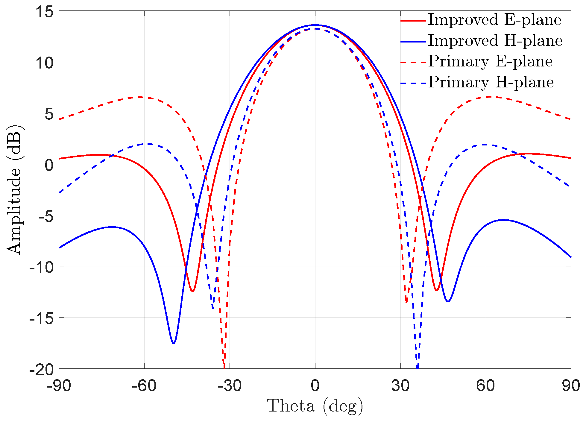
| Frequency (GHz) | E-Plane HPBW (Degree) | H-Plane HPBW (Degree) | E-Plane First SLL (dB) | H-Plane First SLL (dB) |
|---|---|---|---|---|
| 17.9 | 7.01 | 6.87 | −28.9 | −26.1 |
| 20 | 5.46 | 5.74 | −28.3 | −24.8 |
| 22.3 | 4.94 | 4.69 | −28.5 | −20 |
| Ref. | Center Frequency (GHz) | BW (%) | Scale | Peak Gain (dBi) | First SLL (dB) | Aperture Eff (%) | Size (Normalized to ) |
|---|---|---|---|---|---|---|---|
| [33] | 9 | 1.6 | 1 × 10 | 15.6 | −26.3 | N/A | N/A |
| [5] | 10 | 4 | 4 × 4 | 18 | −20 | 72.7 | 2.92 × 2.37 × 0.25 |
| [7] | 37.5 | 17.6 | 8 × 8 | 24..6 | −18 | 34.8 | 6.60 × 6.60 × 0.17 |
| [29] | 7.5 | 31.9 | 1 × 8 | N/A | −24.7 | N/A | 1.05 × 6.25 × 0.24 |
| [19] * | 60 | 20.3 | 16 × 16 | 33.7 | ∼−14 | 74.3 | 16.3 × 15.44 × 1.3 |
| [27] | 15 | 12.6 | 16 × 16 | 30.2 | −24.1 | 58.7 | 12 × 12 × 0.73 |
| [28] | 77 | 13.2 | 64 × 32 | 39.9 | −20.2 | 48.8 | 56.46 × 28.23 × 1.41 |
| This work | 20 | 21.9 | 16 × 16 | 29.1 | −22.5 | 50.6 | 11.31 × 11.31 × 0.48 |
Disclaimer/Publisher’s Note: The statements, opinions and data contained in all publications are solely those of the individual author(s) and contributor(s) and not of MDPI and/or the editor(s). MDPI and/or the editor(s) disclaim responsibility for any injury to people or property resulting from any ideas, methods, instructions or products referred to in the content. |
© 2023 by the authors. Licensee MDPI, Basel, Switzerland. This article is an open access article distributed under the terms and conditions of the Creative Commons Attribution (CC BY) license (https://creativecommons.org/licenses/by/4.0/).
Share and Cite
Yuan, H.; Li, J.; Zhao, Z.; Wang, Z.; Lodi, M.B.; Gugliandolo, G.; Donato, N.; Crupi, G.; Si, L.; Bao, X.
Development of a Wideband Slotted Antenna Array with Low Profile and Low Sidelobe
. Electronics 2023, 12, 278.
https://doi.org/10.3390/electronics12020278
Yuan H, Li J, Zhao Z, Wang Z, Lodi MB, Gugliandolo G, Donato N, Crupi G, Si L, Bao X.
Development of a Wideband Slotted Antenna Array with Low Profile and Low Sidelobe
. Electronics. 2023; 12(2):278.
https://doi.org/10.3390/electronics12020278
Yuan, Haoyun, Jinkai Li, Zhibo Zhao, Zeyu Wang, Matteo Bruno Lodi, Giovanni Gugliandolo, Nicola Donato, Giovanni Crupi, Liming Si, and Xiue Bao.
2023. "Development of a Wideband Slotted Antenna Array with Low Profile and Low Sidelobe
" Electronics 12, no. 2: 278.
https://doi.org/10.3390/electronics12020278