1. Introduction
With the rapid updating and iteration of wireless communication systems, the demand for high-performance modules is becoming more and more urgent [
1]. In view of their characteristics of high output power, wide frequency band, and high efficiency, as a key module of the front end of the whole system, power amplifiers (PAs) have a wide range of applications in mobile communication systems, wireless local area networks, radar, electronic warfare, navigation, and other military and civilian fields, mainly playing an important role in information exchange and transmission [
2]. At the same time, their performance directly affects the efficient, stable, and safe operation and service life of the entire system [
3]. With the popularity of communication base stations, PAs must work in a variety of harsh environments. Especially in extremely harsh conditions, transmission interruption, rapid failure, shutdown and power failure, performance degradation, and other problems occur frequently. It has been reported that for every 10-degree increase in ambient temperature, the probability of failure of electronic components increases by several orders of magnitude [
4]. In other words, temperature is a key factor affecting PA performance [
5]. Devices often operate in a supersaturated state at low temperatures, which will reduce their reliability [
6]. Especially under the high temperature difference in cold conditions, the power transistor temperature is too high because of the difficulty of heat dissipation. This poses a threat to its safe operation and even causes the permanent damage. In general, devices designed according to the electrical characteristics at room temperature cannot meet the requirements of high/low temperature applications. Therefore, it is of great practical significance to study the temperature characteristics of high-power amplifiers for the reliability design of communication systems.
At present, in view of its short switching time, small size, light weight, low cost, high reliability, flexible system design and application, easy maintenance, perfect protection measures, intelligent control, and many other advantages, the all-solid-state transmitter has completely replaced the vacuum tube transmitter. Due to its modular layout and compact structure, the cooling space is relatively small. When the temperature changes, the service life and maintenance costs of the equipment will be greatly affected. However, the performance of PA, on the one hand, is closely related to the linear margin of the amplifier tube; on the other hand, they are also closely related to the operating temperature [
5]. As the core device of PA, the lifetime of the transistor depends on its junction temperature and drain current. In particular, the drain current changes nonlinearly with temperature, resulting in the unstable working state of the transistor, and even affecting the performance of the entire PA. And in practical applications, the threshold voltage of the transistor will decrease with the increase in temperature, which will lead to an increase in the static current and the deterioration of linearity [
6]. At the same time, around the transistor there is more chip resistance, capacitance, and inductance, and the heat output is relatively large, which facilitates excessive temperature increases. As a result, the technical parameters of the PA are abnormal, resulting in an imbalance between the PA modules and increasing the damaged area of the whole module. Therefore, in addition to considering the design concept, technical assurance, processing technology, control technology, and other factors, analyzing the working parameters at different temperatures for high-power PAs is the key to achieving temperature control and ensuring their long-term stability and reliability.
At present, there are some studies on the temperature reliability of RF circuits. In 2001, Ahmed analyzed the relationship between temperature and nonlinearity of PAs from both theoretical and experimental perspectives, which showed that the higher the temperature, the more obvious the nonlinearity [
7]. In 2006, it was confirmed that the internal temperature of RF circuits would affect their stability and reduce their lifetime [
8]. In 2016, Zhao explored the temperature mechanism for a GaN PA [
9]. Meanwhile, it could be seen that its performance was closely related to the transistor, and PA failure caused by thermal effects was more than 50% [
10]. In 2020, the temperature reliability of a Ka-band stacked PA was studied further, and accurate temperature compensation was achieved [
11]. In 2022, a performance analysis of PAs under different conditions of temperature and humidity was completed [
12]. In the same year, Lin deeply studied the temperature degradation law of PAs [
13]. Moreover, considering the differences in circuit structure, integration, device materials, and experimental environment, there have been few studies on the temperature behavior of high-power amplifiers. Therefore, taking a 400 W solid-state PA as an example, temperature reliability under the typical high cold conditions is explored in this paper. Thus, it can provide relatively accurate reference data for subsequent heat dissipation optimization, greatly improve design efficiency, and even shorten the development cycle and reduce costs.
The organization of this paper is as follows: First, the design principle of the 400 W solid-state PA is introduced in
Section 2. Then, the temperature reliability testing of this PA is illustrated in
Section 3, and the experimental results are given in
Section 4. Next, the discussions are presented in
Section 5. Finally, our conclusions are shown in
Section 6.
2. Design Principle of a 400 W Solid-State PA
2.1. Characteristics of LDMOSFETs
Compared with other field-effect transistors, the lateral double-diffused metal–oxide–semiconductor field-effect transistor (LDMOSFET) has obvious advantages of high gain, excellent linearity, switching performance, and heat dissipation, having been widely used in high-power RF circuits. That is, the internal diffusion direction of the conductor is horizontal, and this diffusion method increases the voltage of the transistor, so that it can work stably under high voltages and large currents. As well as being known for high power, high efficiency, and high gain, LDMOSFETs are also anti-reflective and extremely durable. Their gain can be as high as 14 dB or more, and the gain of the power amplifier module produced by it can up to about 60 dB. Therefore, the greater the power of a single power tube, the fewer the number of power tubes used by the amplifier with the same output power. This can greatly reduce the design complexity and the number of circuit boards, as well as the production cost of the transmitter. Moreover, the operating point of LDMOSFETs is sensitive to the grid voltage, and their bias voltage must be regulated by a regulator block. Moreover, as a high-voltage device, they are often applied in RF devices and display driver ICs [
14]. Especially when the temperature changes, it has a zero temperature coefficient (ZTC) point. At the ZTC, two different temperature behaviors are presented [
15]. It also has been shown that when the temperature increases from 20 °C to 100 °C, its quiescent current of I
DQ changes by about 140%. If the temperature is reduced to 0 °C, the change reaches 30% [
16]. The change in I
DQ has a significant impact on the gain, efficiency, and linearity of the PA—especially the linearity, which is the most seriously affected. This is mainly caused by the rising temperature, the increase in the source–drain equivalent resistance of LDMOSFET, and finally lead to the reduction of the drain current of I
DQ. Meanwhile, the drift of I
DQ is also affected by the self-heating effect, which has a great impact on the intermodulation performance of the PA [
17]. Therefore, one of the key points is to maintain the I
DQ constant.
In this paper, the temperature reliability for a 400 W LDMOS solid-state PA is studied. A BHF1D4D 160 W 28 V LDMOSFET and a BHF0DW12D 1100 W 48 V LDMOSFET were adopted in the front-stage driving amplifier circuit and last-stage amplifier circuit for this PA, respectively. These are mainly utilized in HF-1500 MHz shortwave and ultra-shortwave communications or interference, meteorological and aviation radar, ISM applications, analog and digital broadcasting, private network communication base stations, industrial laser sources, and plasma devices [
18]. Furthermore, when the temperature varies from −40 to +100 °C, the drain voltage of V
DS is +60 V and the gate voltage of V
GS is from −3 to +8 V. During the test, the quiescent working condition of the BHF1D4D was set at V
GS = 2.75 V, V
DS = 28 V, and I
DQ = 900 mA, while the working condition of the BHF0DW12D was set at V
DS = 48 V and I
DQ = 200 mA.
2.2. Introduction of the 400 W Solid-State PA
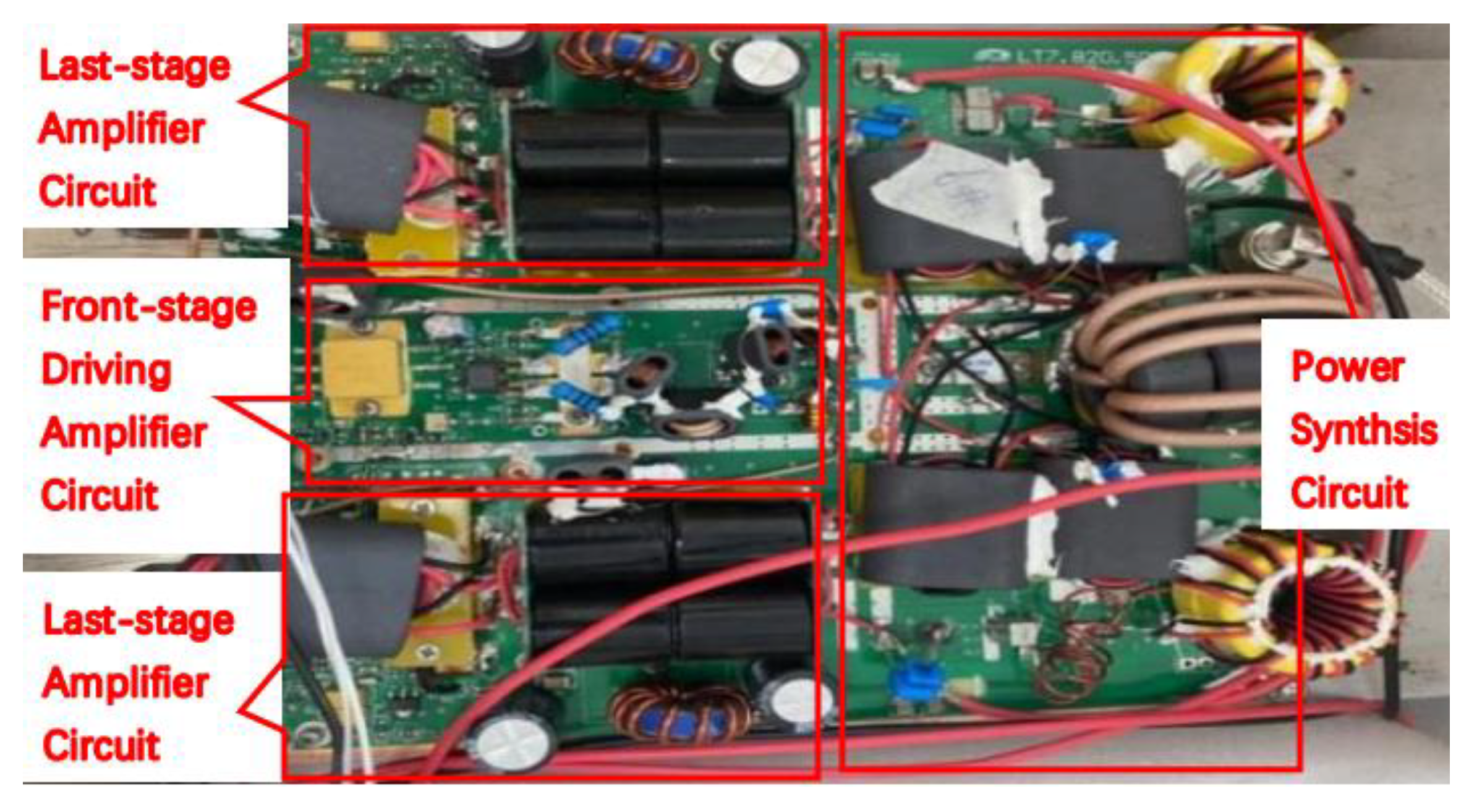
In order to investigate the temperature reliability of high-power amplifiers, a 400 W solid-state PA was selected as the test object. First, a physical photograph of this solid-state PA is presented in
Figure 1. It can be seen that it is mainly composed of three parts: a front-stage driving amplifier circuit, a last-stage amplifier circuit, and a power synthesis circuit.
In addition, a schematic diagram of the front-stage driving circuit is shown in
Figure 2. It starts from the RF input terminal and is connected with two stages of impedance matching and amplifier circuit in turn. The amplifier circuits are connected with the feeding, biasing, and detecting circuits at the same time to provide DC bias for the PA. Their supply voltages are 12 V and 24 V, respectively.
Meanwhile, a schematic diagram of last-stage amplifier circuit is shown in
Figure 3. It starts from the RF input terminal. Then, the input impedance matching, amplifier circuit, and output impedance matching are connected to the RF output terminal in turn. Moreover, the amplifier circuit is connected to the feed and bias circuits, and then connected to the power, temperature, and current detection units to realize the state output with a supply voltage of 36 V.
3. Temperature Reliability Test for This 400 W Solid-State PA
As a result, a series of temperature tests were carried out to determine the temperature characteristics at different temperatures. Because the normal operating temperature range is −40 °C to 55 °C, several temperatures (such as −39.2 °C, −32.9 °C, −25.3 °C, −4.9 °C, 0 °C, 23 °C, and 55 °C) are chosen to represent the high and cold conditions. Among them, −5 °C, −25 °C, −33 °C, and −39 °C represent the lowest temperatures in spring, summer, autumn, and winter in alpine regions, respectively, while 0 °C is the boundary temperature, 23 °C is the average room temperature, and 55 °C is the highest temperature when the circuit works. Meanwhile, in order to ensure the data accuracy, the device was stored at room temperature for 4 h and then powered on for 2 h before testing. Important indices include the drain current of IDS, output power of Pout, gain, power-added efficiency of PAE, the second harmonic, and the third harmonic, among others.
Its test connection diagram is given in
Figure 4. The vector signal generator and spectrum analyzer were applied to observe the RF output signals. Then, the DC power supply was used to provide DC offset for the PA. During the test, this PA was placed in the GDW-010C high and low-temperature test chamber, the allowed temperature range of which is −65,150 °C, with a fluctuation of ±0.5 °C. In particular, it is vital to connect an attenuator of −60 dB to ensure the safety of the instruments and circuits. The actual test environment is shown in
Figure 5.
4. Experimental Results
When the frequency is 16 MHz, the measured curves of I
DS versus Pin at different temperatures are shown in
Figure 6. According to the results, I
DS always increases with the increase in temperature with different DC offsets. In the front-stage driving circuit, its I
DS rises by 0.08 A and 0.05 A under a power supply of 12 V and 24 V, respectively. In the last-stage amplifier circuit, the I
DS at 36 V expands by about 0.06 A.
When the frequency is 2 MHz, the measured curves of Pout, gain, and PAE at different temperatures are as shown in
Figure 7. It can be observed that when temperature increases from −39.2 °C to 55 °C, upward trends are presented for Pout, gain, and PAE. The increases for Pout, gain, and PAE are 3.5 ± 0.5 dBm, 2.5 ± 0.5 dB, and 5%, respectively.
At the frequency of 16 MHz, the measured curves of Pout, gain, and PAE at different temperatures are as shown in
Figure 8. As the temperature increases, the Pout, gain, and PAE all show an upward trend, with increments of 3.0 ± 0.5 dBm, 2.5 ± 0.5 dB, and 5.1%, respectively. Meanwhile, when the temperature is −4.9 °C, its Pout and gain are better than those at 23 °C. Meanwhile, the PAE is extremely higher than that at 23 °C and 55 °C.
At the frequency of 30 MHz, the measured curves of Pout, gain, and PAE at different temperatures are as shown in
Figure 9. Based on the results above, the same trend is presented compared with other frequencies. Its Pout, gain, and PAE rise by about 2 ± 0.5 dBm, 1.5 ± 0.5 dB, and 2%, respectively. Among them, Pout and gain are better at 23 °C, while PAE is higher at 23 °C and 55 °C.
When input power is set to −5 dBm, the measured curves of Pout, gain, and PAE at different temperatures are as shown in
Figure 10. Among them, with the increase in temperature, different trends for Pout and gain are shown. Within the frequency band of 2–10 MHz, the higher the temperature, the better the Pout and gain. In detail, the gain increases by 1 ± 0.5 dB and the Pout rises about 1 ± 0.5 dBm. However, within the frequency band of 10–30 MHz, Pout and gain decrease with the rising temperature. Meanwhile, PAE gradually deteriorates and drops by about 10 ± 1%. Furthermore, the PAE curves tend to be overlapped at −39.2 °C, −32.9 °C, and −25.3 °C.
With an input power of −5 dBm, the measured curves of the second harmonics at different temperatures are as shown in
Figure 11. It can also be seen that with the increasing temperature, the second harmonic decreases, with a reduction of 4 ± 0.5 dBm. Moreover, the second harmonics at −39.2 °C, −32.9 °C, and −25.3 °C are almost overlapped.
Finally, the measured curves of the third harmonic at different temperatures with a Pin of −5 dBm are as shown in
Figure 12. It can also be seen that with the rising temperature the third harmonics become smaller, with a reduction of 4 ± 0.2 dBm. A coincident phenomenon is presented for the third harmonics at low temperatures.
5. Discussions
As presented above, with the increase in temperature from −39.2 °C to 55 °C, IDS increases significantly at all levels. Upward trends are shown for Pout, gain, and PAE at a fixed frequency. When Pin is fixed, Pout and gain increase within the low-frequency band with the increase in temperature. However, the trends are different within the high-frequency band. This is closely related to the existence of the zero temperature coefficient of the LDMOSFET. However, PAE, the second harmonic and the third harmonic drop significantly with the increase in temperature. This is mainly caused by the self-heating effect of the transistor and the limitation of heat dissipation conditions. These can inevitably lead to a drift in the static current and further degrade its Pout, gain, and PAE.
In conclusion, it is deducible that the whole characteristics of the PA are determined not only by the LDMOSFET’s performance, but also by its circuit structure. That is, the temperature behavior of the PA is decided by several factors. Especially, in addition to the circuit structure, the temperature compensation design is the technical bottleneck for LDMOS PAs. As mentioned above, in order to keep the static current (I
DS) constant for LDMOSFET transistors, the bias circuit of LDMOSFET is required to add a temperature compensation part with a temperature coefficient of 3 mV/°C [
19]. Therefore, in order to improve this PA, the bias circuit and temperature compensation circuit can be designed in the final amplifier circuit. Specifically, the temperature compensation circuit can dynamically adjust the bias of the transistor according to the variations in temperature, so that the gain does not follow the change in temperature, and the PA’s stability can be improved. It has been reported that software compensation and hardware compensation are the optimal choices. The former can be achieved with a reasonable software algorithm that is suitable for programmable rewritten digital modules, and the latter can be achieved by adding the peripheral hardware circuits [
20]. For this amplification module, hardware compensation is the best choice.
Furthermore, the final amplifier circuit should be designed with power detection, temperature detection, and current detection. In detail, the power detection circuit can be realized by diode detection mode, which has good consistency and is mature and reliable. It can be built with 7B590 as the core tube, which has high detection accuracy and strong anti-interference. The state detection provides a powerful support and guarantee for state management of the whole module. Furthermore, as for the high-power PA, thermal design is also the crucial problem.
Therefore, in order to ensure the reliability and stability of the transmitter, two aspects must be considered: First, from the perspective of technical indicators, it is necessary to ensure that the power amplifier tube has a sufficient linear power margin, which can not only obtain high indicators, but also reduce the junction temperature and drain current, while also improving the service life of the power amplifier tube. Second, the liquid cooling technology can be used to reduce the junction temperature of the power amplifier tube, so as to extend its service life. With the advantages of high cooling efficiency, environmental protection, low noise, and energy saving, this can exponentially improve the service life and even reduce the failure rate of the transmitter. Thirdly, it is feasible to choose a suitable temperature control circuit with a single-chip microcomputer and use the temperature-sensitive Z element combined with the characteristics of high and cold conditions to control the temperature. In addition, the bias circuit uses a silicon switching diode for temperature compensation, which can effectively stabilize the static working point of the LDMOSFET, so as to ensure the working stability and reliability of the transmitter. Meanwhile, in order to prevent the power amplifier from self-excitation, the output of the power amplifier must be connected to a high-power load before power-on and debugging, and attention must be paid to problems such as matching, filtering, grounding, and taking ESD measures.
6. Conclusions
Considering the differences in circuit structure, integration, device materials, and experimental environment, in order to study the temperature behavior of high-power amplifiers under the typical high and cold conditions, a 400 W solid-state PA was taken as an object and a series of temperature tests were carried out. The test results showed that under a fixed frequency, its Pout, gain, and PAE showed an upward trend with rising temperature. Under a fixed input power, its Pout and gain showed different trends with increasing temperature. Within the frequency band of 2–10 MHz, the higher the temperature, the better the performance. However, within the frequency band of 10–30 MHz, the higher the temperature, the worse the performance. Moreover, the PAE, second harmonic, and third harmonic all showed a decreasing trend. In detail, it can be seen that the degradation and inversion of the PA are most closely related to the zero temperature coefficient and self-heating effect of the LDMOSFET, followed by the thermal design and circuit structure. Finally, hardware compensation is the best choice for reliability design of this high-power PA. Therefore, analyzing the working parameters at different temperatures for high-power PAs is the key to achieving temperature control and ensuring their long-term stability and reliability. This is a necessary supplement and can provide relatively accurate reference data for subsequent heat dissipation optimization and even improve design efficiency, shorten the development cycle, and reduce costs.


