Article

The Design of a Wide-Dynamic-Range and High-Linearity RMS Power Detector for mm-Wave Applications in 65 nm CMOS

1
Shanghai Institute of Microsystem and Information Technology, Chinese Academy of Sciences, Shanghai 200050, China
2
University of Chinese Academy of Sciences, Beijing 100049, China
3
School of Information Science and Technology, ShanghaiTech University, Shanghai 201210, China
4
StorMicro Technologies (Shanghai) Co., Ltd., Shanghai 201899, China
*
Authors to whom correspondence should be addressed.
Electronics 2023, 12(21), 4402; https://doi.org/10.3390/electronics12214402
Submission received: 2 August 2023 / Revised: 4 September 2023 / Accepted: 13 September 2023 / Published: 25 October 2023
(This article belongs to the Special Issue Advanced Design of RF/Microwave Circuit)

Abstract

:
In this paper, a wide dynamic range RMS power detector with an operating frequency from 24 GHz to 35 GHz mm-wave frequency is presented. The power detector is fabricated in a 65 nm CMOS process. It is composed of a power detector unit, a radio frequency signal attenuator and a linear proportional voltage adder. The equalization technique is used to achieve a good linearity performance. The input dynamic range of the power detector is expanded by using one radio frequency signal attenuator and five power detector units. The simulation results show the slope of VOUT versus input power remaining constant at around 0.06 V/dBm when the input signal power varies from −10 dBm to 10 dBm. The difference in output voltage varies by only 0.03 V when the input power varies from −10 to 0 dBm and 0 to 10 dBm. These all indicate that the proposed power detector achieves a good linearity performance. The measured results also show that the proposed power detector achieves a wide dynamic range and a high linearity performance from −10 dBm to 10 dBm. The detectable dynamic range is enhanced by 3.3 times compared to that achieved when only using one single power detector unit, while it only consumes about 0.75 mW under a 1.2 V supply voltage.

1. Introduction

A power detector (PD) plays a vital role in testing and calibrating power that is received or transmitted, and it is widely used in wireless communication systems or radar systems [1,2,3,4,5,6,7,8,9,10]. As shown in Figure 1, the power detector is used to test or calibrate the output power of the power amplifier (PA) or the gain of the low noise amplifier (LNA) [2,4]. The power level of the radio frequency signal can be detected by using the peak or root mean square (RMS) values. An RMS power detector is applied widely with increasing transmission data rates which rely on a high peak average ratio due to its better accuracy [3,4,5].
Several methods have been proposed and applied to improve the performance of power detectors. The method based on electro-thermal coupling is proposed for radio frequency signal power detection in paper [1]. But the detection sensitivity and dynamic range are limited because the electro-thermal sense method needs a diode or bipolar. That is dependent on the process and may not be a standard device in a CMOS process. Thus, this method is not suitable for a system-on-chip applications. One research paper [3] presents a method that adopts the cascading gain amplifiers and the squaring circuits with a power-level segmented detection to achieve a wide dynamic range. However, DC offset also exists in the cascading gain amplifiers. To calibrate this, a 12-bit digital-to-analog converter is included in the power detector, which complicates this whole system and increases the power dissipation. Another method based on the MOS transistor’s weak inversion region achieves linear-in-dB output [4]; the dynamic ranges can reach up to 20 dB at a low frequency of 125 MHz. However, this method is strongly sensitive to the temperature and process variations, its dynamic range and performance are limited, and the dynamic range will decrease with the increase in frequency. The papers [5,6] realized a low-power wide dynamic range radio-frequency power detector, based on a logarithmic amplifier. They achieved about a 50 dB dynamic range of input signal power. However, the RMS amplifier consists of a logarithmic limiting amplifier which has serious DC drift related to temperature. It requires a DC offset cancellation circuit or chopper technology to fix the problem of DC offset and temperature drift; thus, the circuit becomes more complex and expensive. Furthermore, the RMS amplifier’s gain is limited by the input signal frequency. This will cause the sensitivity to weaken and can even cause failure with the increasing operational frequency. Paper [7], which was based on an unbalanced source coupled pair, realized a power detector whose detectable range of input signal power was from −30 dBm to −20 dBm over 0.1–1 GHz. It improved the input sensitivity of the power detector, but the dynamic range is only 10 dB. It still cannot operate at the mm-wave frequency range since the gain of the source coupled pair will also decrease with the increase in frequency. The authors of [8] utilized a programmable voltage bias circuit to change the bias voltage of the NMOS gate-terminal voltage of a power detector unit, which achieves both a wide dynamic peak amplitude range and a wideband capability. However, it requires an extra bias circuit module and algorithm to control the programmable voltage bias circuit, and it detects the radio frequency signal peak amplitude rather than the RMS value. A dynamic range extended method based on a digital control multiple power detector unit was illustrated in [9]. It requires an extra ADC and finite state machine to control the detection unit. The authors of [10] designed a 55 dB dynamic range wideband radio frequency logarithmic power detector according to a SiGe BiCMOS process, using temperature compensation to achieve the temperature-independent transfer characteristics. The authors of [11] utilized reverse received signal strength indicator architecture to dramatically improve the linearity of the power detector. However, the power detector proposed in [10,11] still operates at a low frequency, even when the bandwidth has been expanded to 8 GHz or 10 GHz. In the past few years, mm-wave communication and mm-wave radar applications have started booming, with the use of mm-wave electronic products becoming increasingly widespread. In order to meet the demand for the application of mm-wave radio frequency signal detection, a power detector which can operate at mm-wave frequency range is required. It has also attracted much attention all over the world. The study presented in [12], which is based on a BiCMOS process, realized a mm-wave frequency signal power detector with a dynamic range of 30 dB, but it is not suitable for integration into the standard CMOS process in consideration of the cost and the integration with a large-scale digital circuit. The paper [13] proposed an E-band 40 dB dynamic range multi-tanh power detector in a 0.13 um SiGe process, which can work at a very high mm-wave frequency from 65 to 86 GHz; however, it still uses a SiGe process and the static power consumption is 12 mW under a 2.7 V supply voltage. The authors of [14] demonstrated a single-ended broadband VSWR-resilient joint true power/impedance sensor over 24 GHz to 40 GHz, based on a 45 nm CMOS SOI process. The work in [15] describes a fully differential active power detector based on a Gilbert cell using 0.18 um BiCMOS technology. It operates from 24 GHz to 30 GHz, with a 16 mW static power consumption from a 3.3 V supply voltage. A wideband square law power detector operating between 90 GHz and 140 GHz is presented in [16]. It achieved a 38 dB dynamic range with high-voltage long-channel PMOS transistors under a 5 V supply voltage. The comparatively high supply voltage is not preferred in the low-power applications. These works [12,13,14,15,16] were implemented in SiGe BiCMOS or SOI CMOS with high cost. They are not suitable for large-scale fully integrated applications.
For the low-cost and high-performance mm-wave applications based on fully integrated CMOS technology, this paper proposes a novel RMS power detector, which realizes a wide dynamic range and good linearity from 24 GHz to 35 GHz mm-wave frequency, based on the equalization theory, and combines the multi power detector unit. In Section 2, we will describe the principle of the power detector. In Section 3, we introduce the method of circuit design. The simulation, measurement results, and conclusion are shown in Section 4 and Section 5, respectively.

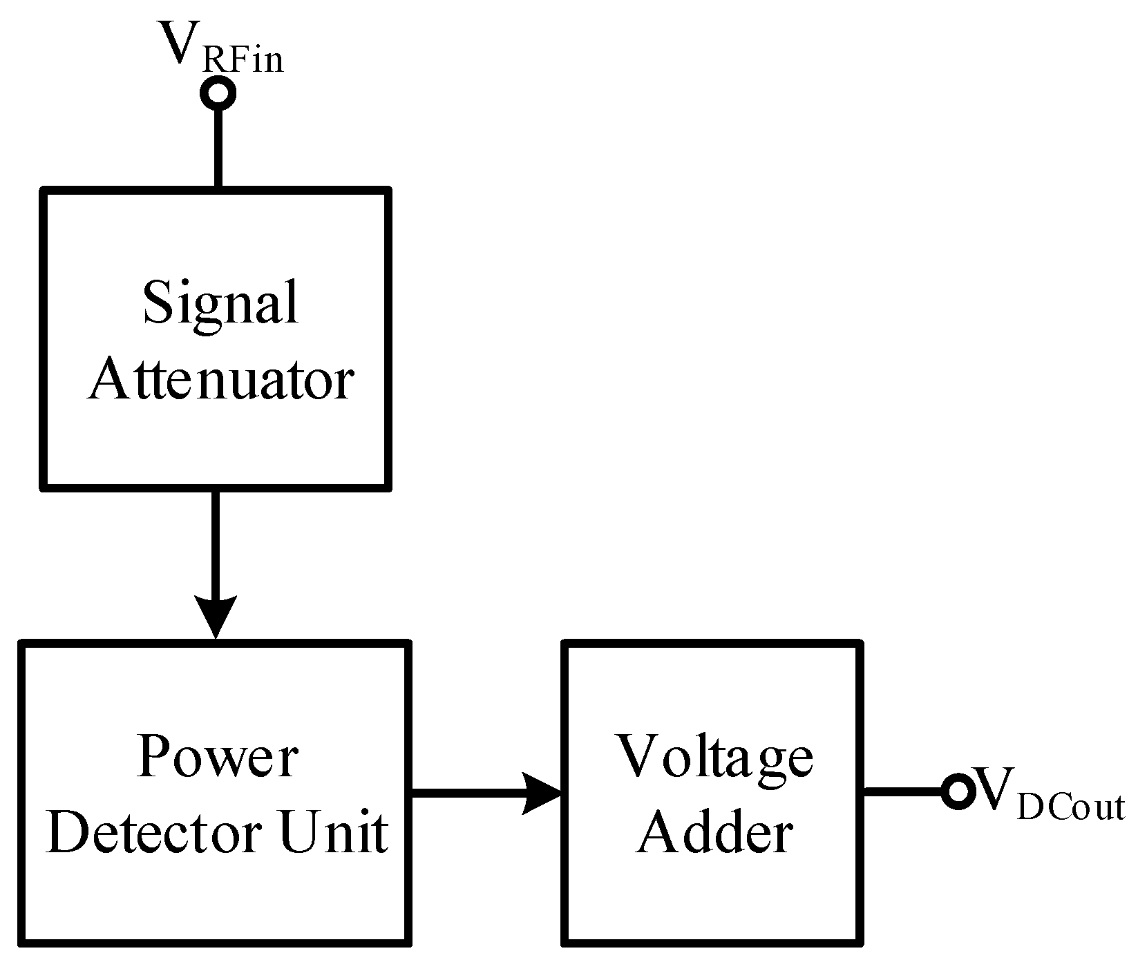
2. The Principle of the Power Detector System

Figure 2 shows the configuration of the proposed power detector system. It consists of a signal attenuator, a power detector unit, and a linear voltage adder. The signal attenuator realizes input radio frequency signal voltage attenuation at a different level, and then transfers to the following power detector unit. The power detector unit is used to detect the power of a signal which has been attenuated. The linear voltage adder based on a rail-to-rail operational amplifier is used to add the output signal of each power detector unit output signal, which helps to achieve a wide-range output.

2.1. The Radio Frequency Signal Attenuator

The signal attenuator consists of a parallel capacitor attenuation array, as shown in Figure 3. It consists of an N-stage parallel capacitor voltage divider. The radio frequency signal attenuator based on a capacitor voltage divider can prevent the equivalent impedance of the power detector input end from affecting the performance of the radio front-end circuit. The N-stage capacitor voltage divider produces attenuated signals VIN1 to VINN, which are proportional to VRF with different attenuation factors. According to the principle of capacitor series voltage divider, we can obtain
V IN s = V RF s C 1 s C 1 + s C 2
Therefore, we can obtain the voltage VIN in a different attenuation proportion to the voltage VRF. The voltage VIN as an input signal is connected to the power detector unit. If the amplitude of VRF is too large to make the power detector work on the saturation region, the voltage VRF can be attenuated to a suitable voltage VIN. The power detector unit works on the linear region via the signal attenuator, so the input dynamic range can be expanded effectively. With more attention, we can design the signal attenuator in a binary or linear method. In this paper, we design the attenuator according to the equalization theory, where five parallel attenuation units are adopted, and a reasonable attenuation factor is set. The factors are 1, 3/4, 1/2, 1/3, and 1/3 from the first attenuator to the last fifth attenuator, respectively. In particular, to achieve the linearity characteristics and expand the dynamic range at the high-power input range, the fourth and fifth attenuators have the same attenuation factor. The attenuation factor is not set, as linearity for the attenuator is a divider of the amplitude of input mm-wave RF signal rather than the divider of the square of the amplitude of input RF mm-wave signal, but the output voltage of the power detector is linearly proportional to the square of the amplitude of the input RF signal. Moreover, these are a set of reasonable factors verified by the simulation carried out in the fourth part of this paper.

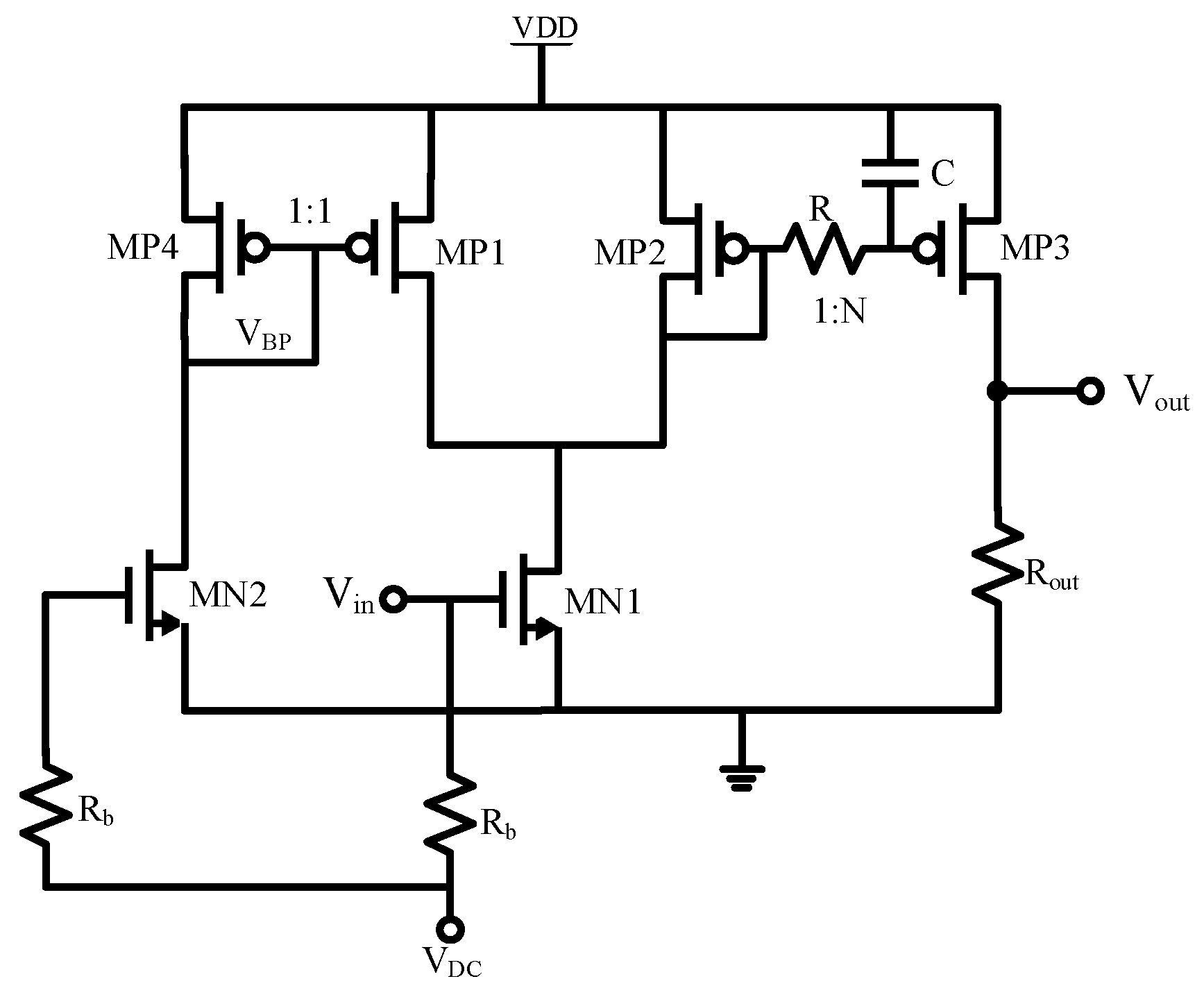
2.2. Power Detector Unit and Equalization Technique

Figure 4 shows the schematic of the power detector unit, which is formed by the NMOS transistors MN1 and MN2; the PMOS transistors MP1, MP2, MP3, and MP4; the resistors Rout, R and Rb; and the capacitor C. The voltage VDC is the DC bias voltage. The voltage Vin is the radio frequency input signal to the basic detection unit circuit which passes through the signal attenuator. Vout is the DC output voltage signal after the power detector unit. The NMOS MN1 and MN2 are biased by common DC voltage VDC, so they have the same DC current. However, the NMOS MN2 also receives the radio signal from the signal attenuator, so the current of MN2 also includes an RF or AC current which is proportional to the power of the input radio signal. The mos-transistors MP1, MP2, and MN1 form a current summing circuit, and the difference current Idiff is achieved after this circuit, which is proportional to the power of the input radio signal. The difference current Idiff flows through the PMOS MP3 and then converts to a voltage by the resistor Rout. The PMOS transistors MP1 and MP4, MP2, and MP3 consist of the current mirror, respectively. The size ratio between (W/L)P1 and (W/L)P4 of MP1 and MP4 is 1:1, and the size ratio between MP2 and MP3 ((W/L)P2:(W/L)P3) is 1:N. Therefore, the difference current is amplified by N through the current mirror formed by MP2 and MP3. The resistor R and the capacitor C form a filter. According to the mos-transistor current square law characteristics, we can obtain
I = 1 2 μ C ox W L ( V gs V th ) 2
where μ is the mobility of charge carriers, Cox is the gate-oxide capacitance per unit area of the mos-transistor, Vgs is the difference voltage between the gate terminal and the source terminal of the mos-transistor, Vth is the threshold voltage of the mos-transistor, and W/L is the width and length ratio of the mos-transistor. We assign K = (1/2) μCoxW/L; according to (2), the current In1 of MN1 is
I n 1 = K ( V DC + V in V th ) 2
According to (2), the current In2 of MN2 is
I n 2 = K ( V DC V th ) 2
Deriving (3)–(4), we can obtain the current difference between
I diff = K V in 2 + 2 K V in V DC V th
For assumption Vin = Vbsin(ωt), where ω is the mm-wave frequency, we assign M = 2K ( V DC V th ) , then
I diff = 1 2 KV b 2 + 1 2 Ksin 2 ω t + 2 M V b sin ω t
Based on Equation (6), we can determine that the current Idiff includes the input RF signal’s RMS power component, first harmonic component and second harmonic component. A low-pass filter formed by a resistor R and a capacitor C is also shown in the power detector unit in Figure 4, where R = 1700 Ω, C = 56 fF, and the parasitic capacitor Cgs among the PMOS transistor MP2 and MP3 will also increase the equivalent capacitance value of the capacitor C. Therefore, it is apparent that the cutoff frequency of this low-pass frequency is lower than 1.6 GHz, according to the calculation formula of cutoff frequency fc = 1/(2πRC). The first harmonic component sin(ωt) and second harmonic component sin(2ωt) can be filtered by the low-pass filter for the frequency ω at mm-Wave frequency range, so only the RMS component is left behind after this low-pass filter has been applied. Equation (6) can be rewritten as
I diff _ DC     1 2 K V b 2 + K V th 2
Thus, according to Equation (7), the current Idiff_DC is a value proportional to the RMS value of the power of the input radio frequency signal Vin. The Idiff_DC is amplified N times by the current mirror, which consists of MP2 and MP3. In other words, the current IMP3 of MP3 is N × Idiff_DC, and the current IMP3 flows to the resistor R and converts to output voltage Vout. According to Equations (2)–(7), the Vout is proportional to the power of the input radio frequency signal. To obtain a good performance, we need to keep the mos-transistors MN1 and MN2, MP1 and MP4, MP2 and MP3 matched, which can be achieved with a careful layout.
Most importantly, the sensitivity is also key to the performance of the power detector. Thus, in order to achieve a higher sensitivity, the power detector needs a large conversion gain [4,5]. However, a too-large conversion gain will cause the power detector to enter the saturation region at a lower-input power level compared to the small conversion gain. This means that the input dynamic will be narrowed, as shown by Figure 5a. It is apparent that there is a trade-off between sensitivity and input dynamic range. The trade-off between sensitivity and conversion gain can be broken down based on the equalization theory and technique. Firstly, the equalization technique uses multiple high-conversion gain power detector units, making them work at different input power levels of the RF mm-wave signal. In addition, the higher the power of the input RF mm-wave signal, the larger the attenuation factor is set to the signal attenuation; thus, the high power is shrunk and input to the power detector. Finally, each power detector unit can work at a suitable level of power. Therefore, the sensitivity and dynamic range can be achieved. On the other hand, the equalization technique causes the linear region of each power detector unit to overlap with one other. Therefore, the linear region of the whole power detector is also expanded compared to that only using a single power detector unit, as shown by Figure 5b. The comparison between the power detector without and with the equalization technique is also shown in Figure 5. Overall, using this method, we can obtain both the sensitivity and input dynamic range, and the linear region of the power detector is also expanded.

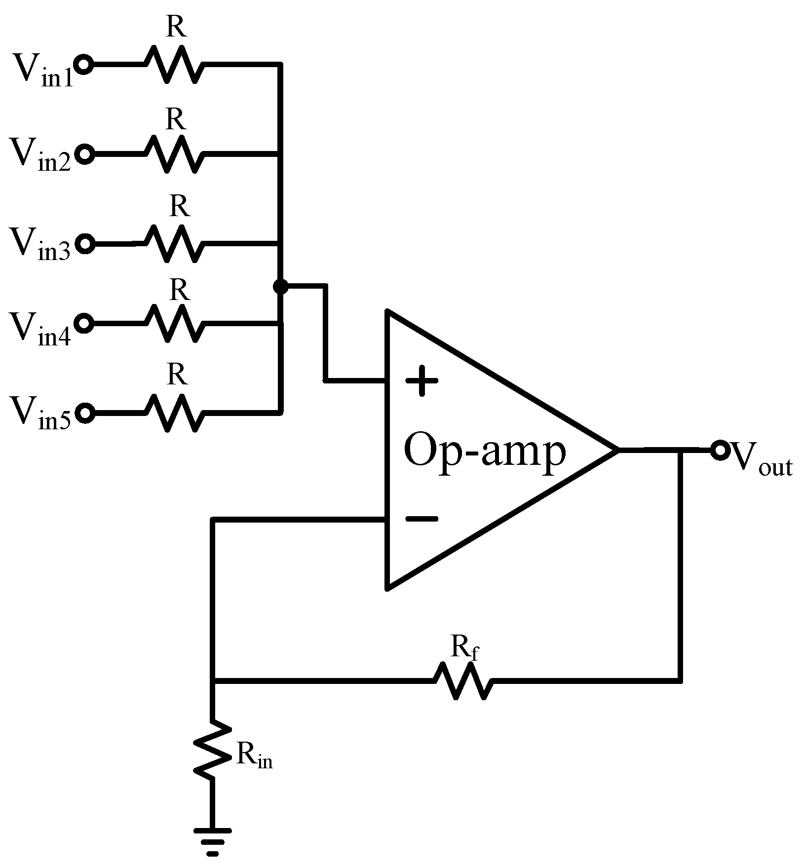
2.3. The Linear Proportional Voltage Adder

In [10,11], the multi-rectifier is used to produce a current that is proportional to the power of the radio frequency signal. The current from each rectifier flows through a resistor, then converts to the voltage which is proportional to the radio frequency signal’s power. However, if the output voltage is larger, this method is limited by the supply voltage. A too-large output voltage will push the rectifier coming into the saturation region. This will cause the dynamic range of the input signal power to become narrow. Therefore, we proposed a linear proportional voltage adder to solve this problem. Using the linear proportional voltage adder, we can combine the output voltage of each stage power detector unit, rather than the current. This keeps each stage power detector unit working in the linear region to achieve good linear characteristics. The linear proportional voltage adder is based on a rail-to-rail operational amplifier to obtain a wide voltage range for the input and output voltage. The schematic is shown in Figure 6, which consists of resistor R, Rin, Rf, and the rail-to-rail operational amplifier. The signals Vin1, Vin2, Vin3, Vin4, and Vin5 are from each power detector unit output, and the Vout is the output voltage of the proposed whole power detector. According to the virtual short principle, we can obtain
V out = R f R ( V in 1 + V in 2 + V in 3 + V in 4 + V in 5 )
A too-large output voltage for each power detector can be avoided effectively by using the linear proportional voltage adder. Thus, the power detector can detect a wide enough range of the power of the input radio frequency signal. It is necessary to focus on ensuring that the resistance value of the resistor R is large enough to ensure sufficient gain for each power detector unit.

3. Design and Implementation of the Proposed Power Detector

Based on the technique proposed in Section 2, we design a wide-input dynamic range with a high-linearity RMS power detector based on a 65 nm CMOS process. This proposed power detector supports 24 GHz to 35 GHz mm-wave frequency operation. The schematic of the proposed power detector is shown in Figure 7. To achieve a wide-input dynamic range, we adopt five parallel attenuators with different attenuation factors and five parallel detector units according to the equalization technique described in Section 2. Thus, there is always a power detector working on the suitable linear region when the input radio frequency signal is observed after five parallel attenuators. The linear proportional adder also has five inputs which connect to five power detector unit outputs, allowing five outputs from the power detector unit to be added together linearly. We can avoid using only a single resistor to convert the DC current to DC voltage of each power detector unit by using a linear proportional adder. This will prevent all power detector unit output stages working at the saturation region even if the power level is not too high. If each power detector works into a saturation region, the sensitivity and dynamic range of the power detector will be seriously degraded. Furthermore, to reduce the power consumption, the branch is formed by MN1, MP4 and Rb, which can be reused to bias each power-detector unit. In order to obtain good robustness performance, this bias branch, which generates voltage bias VBP for each power detector unit, is replaced by a feedback loop. This feedback loop, which is known as the VBP generating circuit, consists of a replica cell which is consistent with the power detection unit and an op-amp; this module is shown in the blue block in Figure 7. The replica power detector unit is only biased by the same DC voltage in the input with the power detector unit, which is used in the detection path of mm-wave signal power. The output of the replica power detector unit is output to the amplifier input. The output voltage of the amplifier VBP feeds back to the gate terminal of MOS transistor MP1 of the replica power detector, as well as to the bias voltage supply to the other power detector. This VBP-generated circuit can cause the power detector circuit unit and the replica power detector circuit unit to all have the same DC bias voltage, which is controlled by the feedback loop. Therefore, the current of MP1 must be equal to the current of MN1 rather than differing for the channel length modulation effect. It should be noted that this feedback loop can avoid the PVT difference between MOS that causes the decrease in detector accuracy. The stability simulation result of the feedback loop of the VBP-generated circuit is shown in Figure 8. This shows that the phase margin of the feedback loop is more than 80 degrees, which ensures the stability of the feedback loop. As we know, the DC offset will be amplified by the cascade amplifier. Since the five power detect units are paralleled, the DC offset will be negligible compared to the method which adopts the cascading gain amplifiers [3] or the logarithmic amplifiers [5,6]. We planned the layout of the proposed RMS power detector carefully, to ensure a good match for each key model. The die micrograph of the proposed power detector test unit is shown in Figure 9.

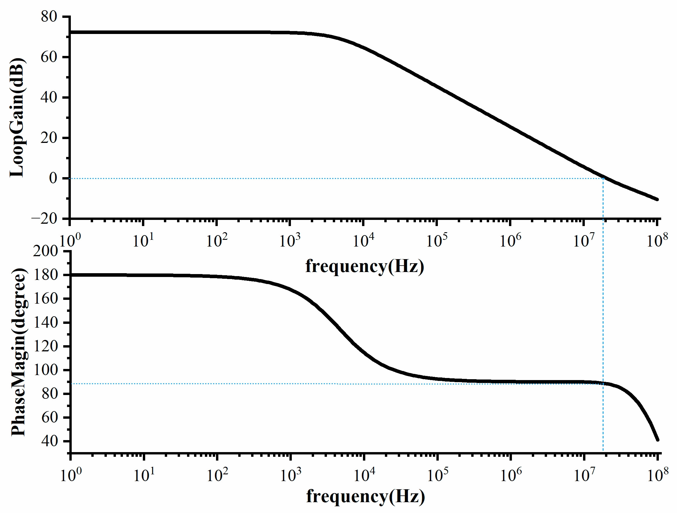
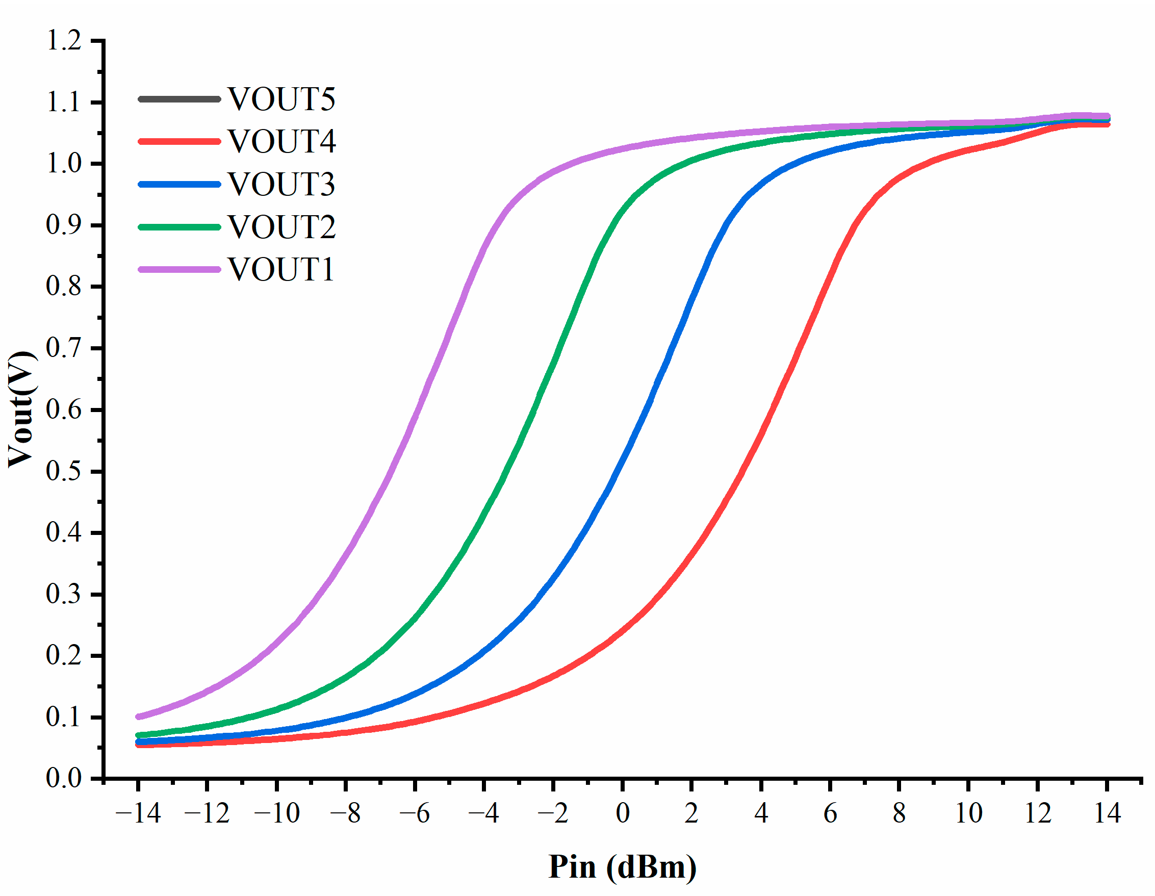
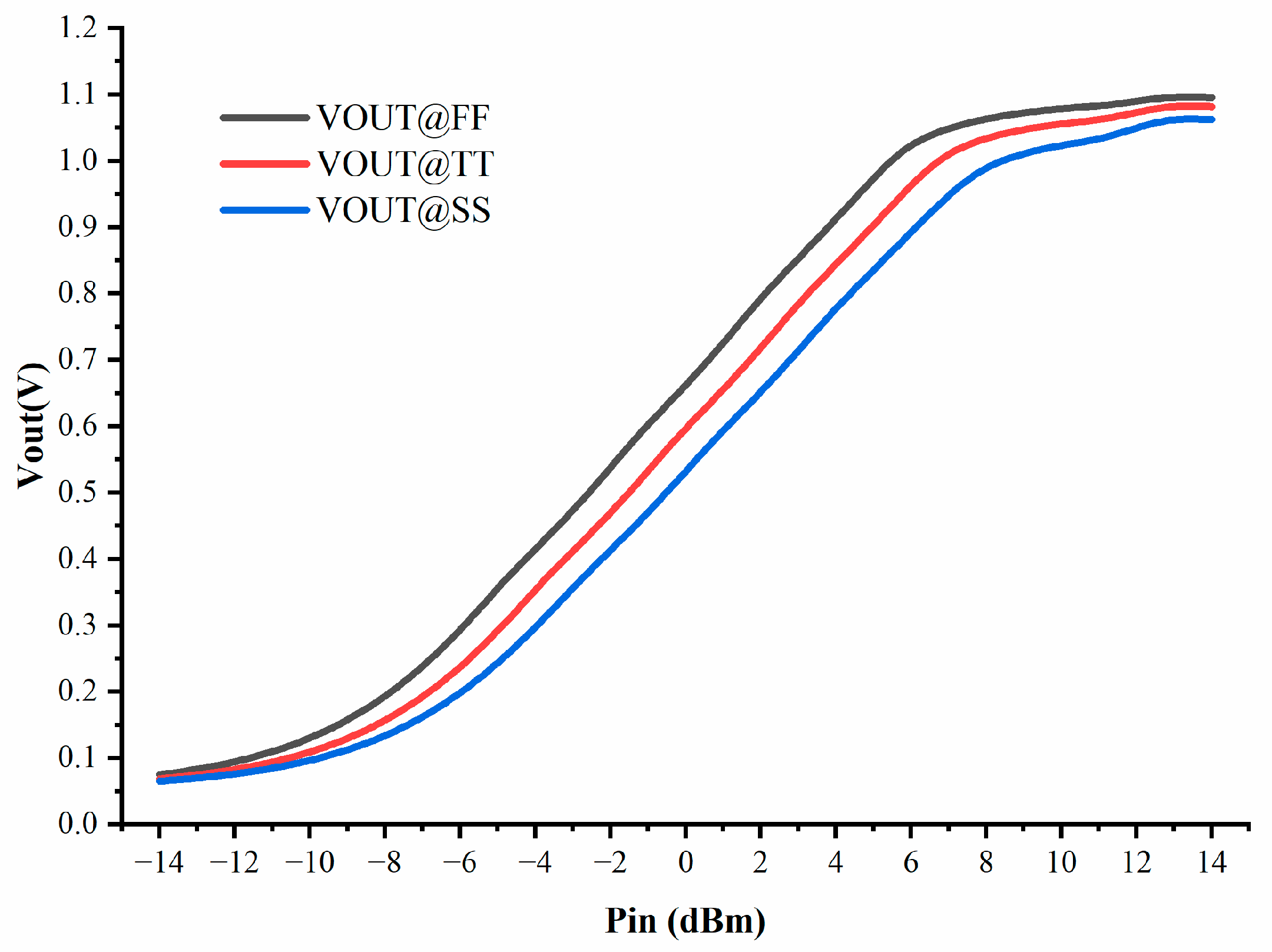
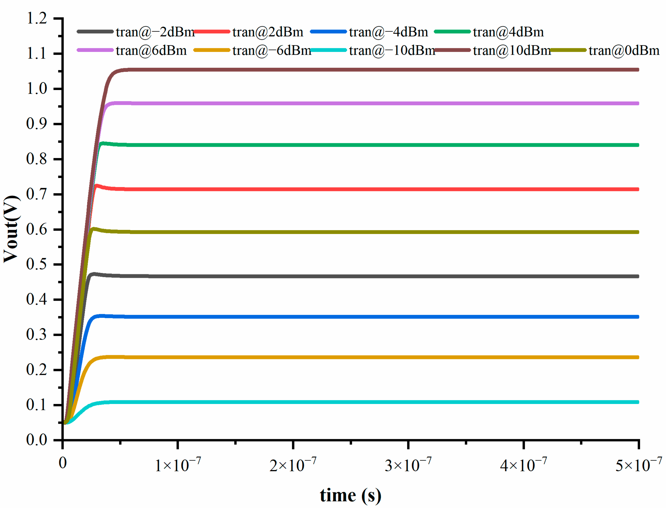
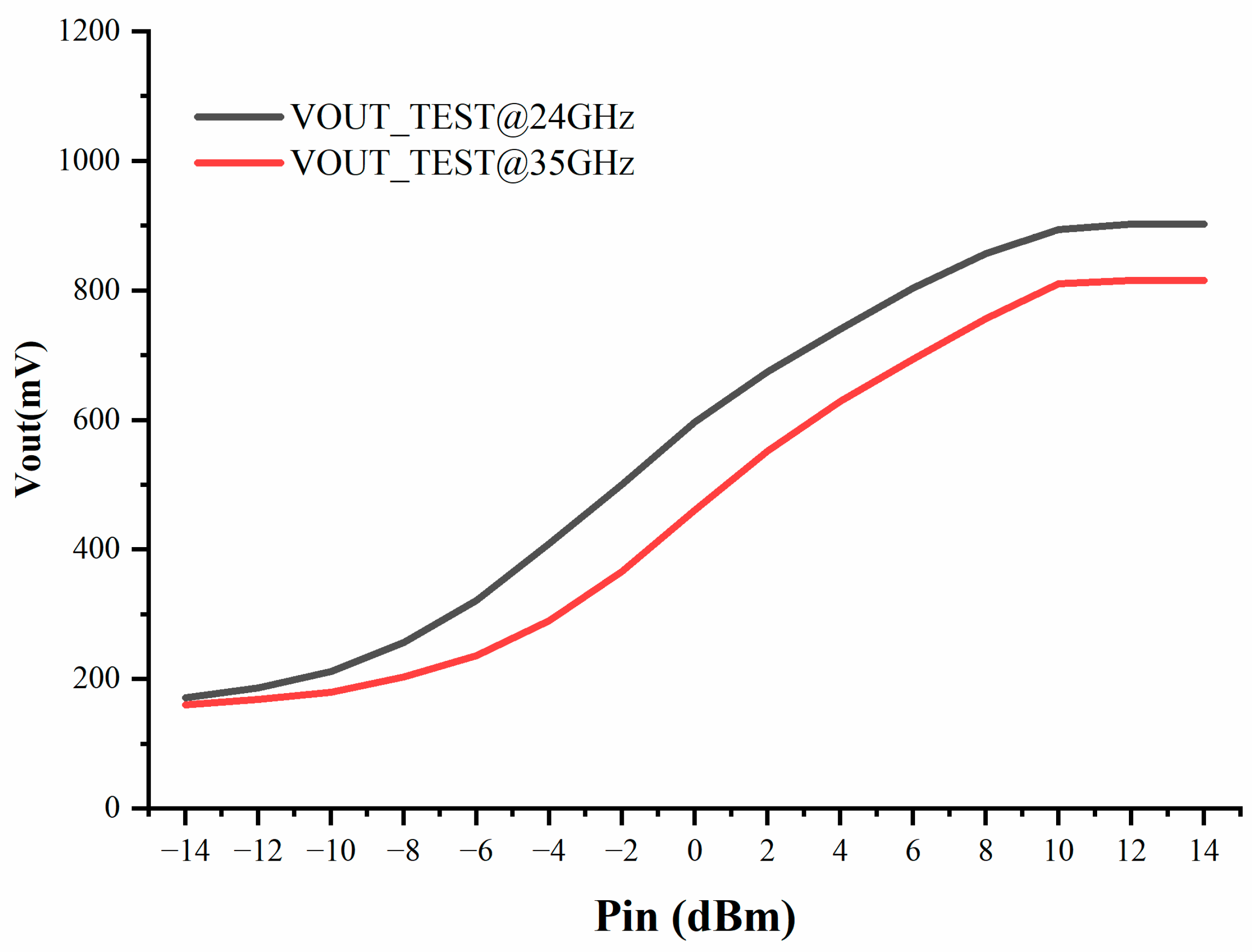
4. Simulation and Measurement Results

The simulation and measurement are carried out to verify the performance of the proposed power detector at a 1.2 V supply voltage. Figure 10 shows the simulation results of each power detector unit output voltage change versus the power variation in the input signal at 24 GHz. The output voltages are VOUT1, VOUT2, VOUT3, VOUT4 and VOUT5, which originate from five parallel power detector units. The VOUT1 versus input power has a linear feature in the range from −10 dBm to −4 dBm. The VOUT2 versus input power has a linear feature in the range from −6 dBm to −2 dBm. The VOUT3 versus input power has a linear feature in the range from −4 dBm to 2 dBm. The VOUT4 and VOUT5 versus input power have a linear feature in the range from 0 to 6 dBm. It can be seen that the output of one single power detector unit features a narrow linear range of about 6 dB. There are 2 dB-wide overlaps between the curves of output voltages that are adjacent to each other, which is featured with linear characteristics. As mentioned previously, they have the same characteristics between the output voltage curve of the fourth and the fifth power detector units for the fourth and the fifth attenuators have the same factor, allowing them to obtain an expanded input dynamic range at a high-power input range. Figure 11 is the output of the proposed power detector with the equalization technique under the different corners. The detectable range of input power is from −12 dBm to 14 dBm, and the range featured with linearity is from −10 dBm to 10 dBm, about 20 dB. The range featured with linearity is about 3.3 times greater than that achieved when only one single power detector is used, and the output voltage is from 80 mV to 1.1 V. This indicates that the proposed power detector has a wider dynamic range of input radio frequency signal power compared with Figure 10. There is a difference of 69 mV and 62 mV between ss and tt, ff and tt, which shows that a good robust performance is achieved. Figure 12 compares the slope of the output of the proposed power detector and the slope of the output of each power detector unit. K1, K2, K3, K4, and K5 stand for the slope of each power detector unit output. We find that the slope of each power detector unit varies from about 0.01 V/dBm to about 0.12 V/dBm, which is a quite large variation. The Ktot is the slope of the proposed power detector; we find that the slope of VOUT versus input power remains constant at around 0.06 V/dBm when the power of input radio frequency from −10 dBm changes to 10 dBm. Comparing the slope of the output voltage between each single power detector unit and the proposed whole power detector output, we find that the proposed power detector with the equalization technique achieves a wide input dynamic range of radio frequency signal power, and the linear characteristics are improved effectively. Figure 13 shows the transient simulation result of the proposed power detector; from this simulation result, we can determine that the output voltage is about 0.11 V, 0.59 V and 1.05 V at −10 dBm, 0 dBm and 10 dBm, respectively. The difference of output voltage when input power varies between −10 dBm and 0 dBm is 0.48 V, and the difference of output voltage when input power varies between 0 dBm and 10 dBm is 0.46 V, so there is only about 0.02 V variation. The results show that the variation of the output voltage is almost the same, when the input power changes an equal amount. These simulation results also indicate that the proposed power detector achieves good linear characteristics by adopting equalization technology. Figure 14 shows the measurement result of the power detector versus input power at different frequency; it shows that the proposed power detector can detect signal power from −14 dBm to 12 dBm over 24 GHz to 35 GHz mm-wave frequency and presents a good linearity performance from −10 dBm to 10 dBm compared to that of a single power detector unit. This figure also reveals that the detectable linear dynamic range is enhanced by 3.3 times compared to that achieved when using only one single power detector unit from the measurement result. Table 1 compares the performances of the proposed wide dynamic range and high-linearity power detector with other power detectors which have been described in the literature. Based on this comparison, we find that this work achieves a wide dynamic range and good linearity over 24 GHz to 35 GHz mm-wave frequency range in the standard CMOS process. It should be mentioned that if more power detector units and a signal attenuator are used in the design, a wider dynamic range can be achieved, but more power consumption is required.

5. Conclusions

An RMS power detector in a 65 nm CMOS process for mm-wave application has been introduced in this work. Based on the equalization technique, the multi-unit parallel detect method, the replica PD unit feedback loop and the linear proportional voltage adder, it reaches a wide dynamic range and high-linearity performance. The simulation and measurement results show that this power detector achieves about 20 dB input dynamic range from 24 GHz to 35 GHz mm-wave frequency. It only consumes about 0.75 mW under a 1.2 V supply voltage. Moreover, the dynamic range can also be further expanded by adding another power detector unit or pre-amplifier with more power dissipation. This work indicates the feasibility of the wide-input dynamic range power detector with good linearity performance in the standard CMOS. It can be applied to auto-calibrate or measure the power of radio frequency signal in mm-wave radar or another wireless communication system with greater area and cost savings.

Author Contributions

Conceptualization, X.-A.W.; methodology, X.-A.W.; validation, X.-A.W.; formal analysis, X.-A.W.; investigation, X.-A.W.; resources, T.T.; data curation, X.-A.W.; writing—original draft preparation, X.-A.W.; writing—review and editing, Z.Z., H.L. and T.T.; visualization, X.-A.W., Z.Z. and H.L.; supervision, T.T.; project administration, T.T. All authors have read and agreed to the published version of the manuscript.

Funding

This research received no external funding.

Data Availability Statement

Data are contained within the article.

Conflicts of Interest

The authors declare no conflict of interest.

References

  1. Feng, J.; Onabajo, M. Wide Dynamic Range CMOS Amplifier Design for RF Signal Power Detection via Electro-Thermal Coupling. J. Electron. Test. 2014, 30, 101–109. [Google Scholar] [CrossRef]
  2. Wu, G.; Belostotski, L.; James, W.H. A 65 nm CMOS broadband self-calibrated power detector for the square kilometre array radio telescope. J. Eng. 2014, 2014, 494–502. [Google Scholar] [CrossRef]
  3. Choi, J.; Lee, J.; Xi, Y.; Myoung, S.S.; Baek, S.; Kwon, D.H.; Bui, Q.D.; Lee, J.; Oh, D.; Cho, T.B. Wide Dynamic-Range CMOS RMS Power Detector. IEEE Trans. Microw. Theory Tech. 2016, 64, 868–880. [Google Scholar] [CrossRef]
  4. Zhou, Y.; Chia, Y.W. A Low-Power Ultra-Wideband CMOS True RMS Power Detector. IEEE Trans. Microw. Theory Tech. 2008, 56, 1052–1058. [Google Scholar] [CrossRef]
  5. Sakphrom, S.; Thanachayanont, A. A low-power CMOS RF power detector. In Proceedings of the 2012 19th IEEE International Conference on Electronics, Circuits, and Systems, Seville, Spain, 9–12 December 2012; IEEE: Piscataway, NJ, USA, 2013. [Google Scholar]
  6. Zhou, Y.; Wah, M. A wide band CMOS RF power detector. In Proceedings of the 2006 IEEE International Symposium on Circuits & Systems, Kos, Greece, 21–24 May 2006; IEEE: Piscataway, NJ, USA, 2006. [Google Scholar]
  7. Hangue, P.A.R.K.; Jaejun, L.E.E.; Jaechun, L.E.E.; Sangwook, N.A.M. A CMOS RF Power Detector Using an Improved Unbalanced Source Coupled Pair. IEICE Trans. Electron. 2009, 91, 1969–1970. [Google Scholar]
  8. Sleiman, S.B.; Ismail, M. A CMOS amplitude detector for RF-BIST and calibration. In Proceedings of the 2009 16th IEEE International Conference on Electronics, Circuits and systems, Yasmine Hammamet, Tunesia, 13–19 December 2009; IEEE: Piscataway, NJ, USA, 2010. [Google Scholar]
  9. Richardson, F.D.; Kouki, A.B.; Gagnon, G. A CMOS RF power detector for an Automatic Impedance Matching System. In Proceedings of the 2011 9th IEEE International New Circuits & Systems Conference, Bordeaux, France, 26–29 June 2011; IEEE: Piscataway, NJ, USA, 2011. [Google Scholar]
  10. Jiang, Y.; Liu, X.; Zhang, Q.; Su, X.; Yu, Z.; Zhang, H. A 55-dB Dynamic Range Wideband RF Logarithmic Power Detector with Temperature and DC Offset Compensation. IEICE Electron. Express 2021, 18, 20200426. [Google Scholar] [CrossRef]
  11. Wang, J.; Zheng, Y.; Yang, F.; Liao, H. A wide band CMOS radio frequency RMS power detector with 42-dB dynamic range. In Proceedings of the 2015 IEEE International Symposium on Circuits & Systems, Lisbon, Portugal, 24–27 May 2015; IEEE: Piscataway, NJ, USA, 2015. [Google Scholar]
  12. Serhan, A.; Lauga-Larroze, E.; Fournier, J.M. A 700 MHz output bandwidth, 30 dB dynamic range, common-base mm-wave power detector. In Proceedings of the 2015 IEEE MTT-S International Microwave Symposium, Phoenix, AZ, USA, 17–22 May 2015; IEEE: Piscataway, NJ, USA, 2015. [Google Scholar]
  13. Levinger, R.; Katz, O.; Sheinman, B.; Carmon, R.; Ben-Yishay, R.; Mazor, N.; Pivnik, S.; Elad, D.; Socher, E. An E-band 40 dB dynamic range multi-tanh power detector in 0.13 μm SiGe technology. In Proceedings of the 2014 9th European Microwave Integrated Circuit Conference, Rome, Italy, 6–7 October 2014; IEEE: Piscataway, NJ, USA, 2014; pp. 170–173. [Google Scholar]
  14. Munzer, D.J.; Mannem, N.S.; Garay, E.; Wang, H. A Broadband Mm-Wave VSWR-Resilient Joint True-Power Detector and Impedance Sensor Supporting Single-Ended Antenna Interfaces. In Proceedings of the 2022 IEEE International Solid-State Circuits Conference (ISSCC), San Francisco, CA, USA, 20–26 February 2022; IEEE: Piscataway, NJ, USA, 2022. [Google Scholar]
  15. Amer, A.E.; Ashry, A.; Abdalla, M.A.Y.; Eshrah, I.A. Gilbert Based Power Detector for 5G mm-Wave Transceivers Built-in-Self Test. In Proceedings of the 2019 IEEE International Symposium on Circuits and Systems (ISCAS), Sapporo, Japan, 26–29 May 2019; IEEE: Piscataway, NJ, USA, 2019. [Google Scholar]
  16. Stärke, P.; Rieß, V.; Fritsche, D.; Carta, C.; Ellinger, F. A wideband square-law power detector with high dynamic range and combined logarithmic amplifier for 100 GHz F-Band in 130 nm SiGe BiCMOS. In Proceedings of the 2017 IEEE Bipolar/BiCMOS Circuits and Technology Meeting (BCTM), Miami, FL, USA, 19–21 October 2017; IEEE: Piscataway, NJ, USA, 2017. [Google Scholar]
Figure 1. The application of the power detector.
Electronics 12 04402 g001
Figure 2. The system graph of the proposed power detector.
Electronics 12 04402 g002
Figure 3. The radio frequency signal attenuator.
Electronics 12 04402 g003
Figure 4. The schematic of the basic power detector unit.
Electronics 12 04402 g004
Figure 5. The concept figure of comparison between power detectors without and with equalization technique (a,b).
Electronics 12 04402 g005
Figure 6. The linear proportional voltage adder based on an operational amplifier.
Electronics 12 04402 g006
Figure 7. The key structure of the proposed PD.
Electronics 12 04402 g007
Figure 8. The loop stability simulation result of the bias voltage VBP-generated circuit.
Electronics 12 04402 g008
Figure 9. The die micrograph of the proposed PD.
Electronics 12 04402 g009
Figure 10. The output voltage of each PD unit output at 24 GHz.
Electronics 12 04402 g010
Figure 11. The result of the output of the proposed PD with equalization technique at 24 GHz under different corners.
Electronics 12 04402 g011
Figure 12. The comparison of slope between each PD unit and the whole power detector.
Electronics 12 04402 g012
Figure 13. The transient output of PD with different input power.
Electronics 12 04402 g013
Figure 14. The measurement results of PD versus different input power.
Electronics 12 04402 g014
Table 1. The performance comparison with other state-of-the-art RF PDs.
2016
[3]
2021
[10]
2015
[12]
2014
[13]
This Work
Process28 nm
CMOS
180 nm
SiGe BiCMOS
55 nm
BiCMOS
130 nm
SiGe
BiCMOS
65 nm
CMOS
Operating frequency/GHz0.7–40.001–850–6665–8624–35
Dynamic range/dB40>5030>4024
Power consumption/mW5.8–11.8680.08120.75
Disclaimer/Publisher’s Note: The statements, opinions and data contained in all publications are solely those of the individual author(s) and contributor(s) and not of MDPI and/or the editor(s). MDPI and/or the editor(s) disclaim responsibility for any injury to people or property resulting from any ideas, methods, instructions or products referred to in the content.

