Article

Digitalized Control Algorithm of Bridgeless Totem-Pole PFC with a Simple Control Structure Based on the Phase Angle

1
Department of Electrical Engineering, Gyeongsang National University, Jinju 52828, Republic of Korea
2
The Department of Electrical and Biomedical Engineering, Hanyang University, Seoul 04763, Republic of Korea
*
Author to whom correspondence should be addressed.
Electronics 2023, 12(21), 4449; https://doi.org/10.3390/electronics12214449
Submission received: 18 September 2023 / Revised: 25 October 2023 / Accepted: 28 October 2023 / Published: 29 October 2023
(This article belongs to the Section Power Electronics)

Abstract

:
Compared to the conventional boost power factor correction (PFC) converter, a totem-pole bridgeless PFC has high efficiency because it does not have an input diode rectifier stage, but a current spike may occur when the polarity of the grid voltage changes. This paper proposes a digital control algorithm for bridgeless totem-pole PFC with a simple control structure based on the phase angle of grid voltage. The proposed algorithm has a PI-based double-loop control structure and performs DC-link voltage and input inductor current control. Rectifying switches operate based on the proposed rectification algorithm using phase angle information calculated through a single-phase phase-locked loop (PLL) to prevent current spikes. The feed-forward duty ratio value is calculated according to the polarity of the grid voltage and added to the double-loop controller to perform appropriate power factor control. The performance and feasibility of the proposed control algorithm are verified through a 3 kW hardware prototype.

1. Introduction

In the power electronics field, power factor correction (PFC) converters are widely used in various industrial areas, such as network server power [1,2], electric vehicle chargers [3,4,5], and LED drivers [6,7,8]. Power conversion systems must meet harmonic regulations in international standards such as IEC 61000-3-2 [9]. Therefore, PFC converters have been essential for the power factor control of an AC grid and stable DC voltage supply.
In the modern power conversion industry, there has been a continuous need to achieve high efficiency converters [10,11,12]. Among the boost PFC topologies, there are various topologies such as single-switch boost PFC [13], semi-bridgeless PFC [14], and interleaved boost PFC [15]. These topologies essentially require diodes to rectify the grid voltage and, accordingly, bridge-less topologies that do not use diode bridges have been researched. Among them, the totem-pole bridge-less PFC (TBPFC) topology is proposed. TBPFC comprises two switches operating at high frequency, two operating slowly according to the grid voltage frequency, and one inductor as shown in Figure 1. In particular, it does not have a rectifier diode in the front end, and two low-speed switches are responsible for the rectification operation. Furthermore, it is operated through only two high-speed switches controlled by the main duty ratio. Therefore, TBPFC can achieve high efficiency due to low conduction and switching loss and high power density due to its simple circuit configuration [16,17,18].
The control system configuration of PFC is generally a two-loop system, with a voltage controller in the outer loop and a current controller in the inner loop. The control system usually uses proportional-integral (PI) control, and three main methods are mainly used for switching modulation: continuous conduction mode (CCM), discontinuous conduction mode (DCM), and critical conduction mode (CrM) control. In CCM control, the current continuously flows through the inductor at a fixed switching frequency and is controlled in a sinusoidal shape. This method has low peak values of current, resulting in low conduction losses, and the requirements for switches are also relatively small [19]. In DCM control, the inductor current is controlled discontinuously by repeatedly going back and forth between the current command and zero current. Due to this operation, zero voltage switching (ZVS) can be achieved, there is no reverse recovery of the diode, and the switching frequency can be changed depending on the phase [20]. In CrM control, the inductor current repeatedly goes back and forth between the current command and zero current, but the current is controlled continuously without a zero-current section. CrM control also has no losses due to the diode reverse recovery phenomenon. It can reduce the size of the inductor by doubling the ripple of the inductor current, thereby improving power density [21]. However, when operating DCM or CrM, it is difficult to apply to high-power applications due to high conduction loss. Accordingly, CCM control, which has a general purpose, is widely used for PFC control.
Various control methods have been proposed for the stable operation of TBPFC. In [22,23], a digital notch filter is applied to remove the 120 Hz component of sensed DC-link voltage, and in [24], the authors presented a 120 Hz reduction method of the input current by adding a notch filter between the voltage and the current controller. To reduce a zero-current spike current, a partial open-loop operation method is proposed [25,26]. This method operates high-frequency switches to a predefined duty ratio at rectification. In [27], a DC bus feed-forward and variable gain control method based on the DC-link voltage is proposed. A current control loop operates independently, with the DC-link voltage, from this control method. In [28], a model predictive current controller is proposed. An appropriate current shaping and ripple reduction is achieved by variable sampling time. In [29], a polarity detection algorithm based on the sensed grid voltage is proposed. The sensed current value is reversed when the grid voltage is in a negative cycle, to control positive and negative inductor current control. These conventional methods are relatively complicated to implement, so simplification is necessary.
In this paper, a digitalized control algorithm for TBPFC with a simple control structure that can minimize zero-current spikes is proposed. The proposed algorithm has a PI-based double-loop control structure and performs DC-link voltage and input inductor current control. In addition, control and rectification switch operation sequences are implemented through phase angle information of the grid voltage to prevent zero-current spikes without complicated sequences. The phase information of the grid voltage is extracted through a general single-phase phase-lock loop (PLL). Additionally, a feedforward technique is applied to reduce the output of closed-loop controllers. The feedforward duty value is used according to the polarity of the grid voltage and performs appropriate power factor control accordingly. The contents of this paper are as follows. Section 2 analyzes the operating principle of TBPFC. Section 3 covers the details of the proposed algorithm. Section 4 presents experimental results to verify the feasibility of the proposed algorithm. The performance of the proposed control algorithm is verified through a 3 kW hardware prototype.

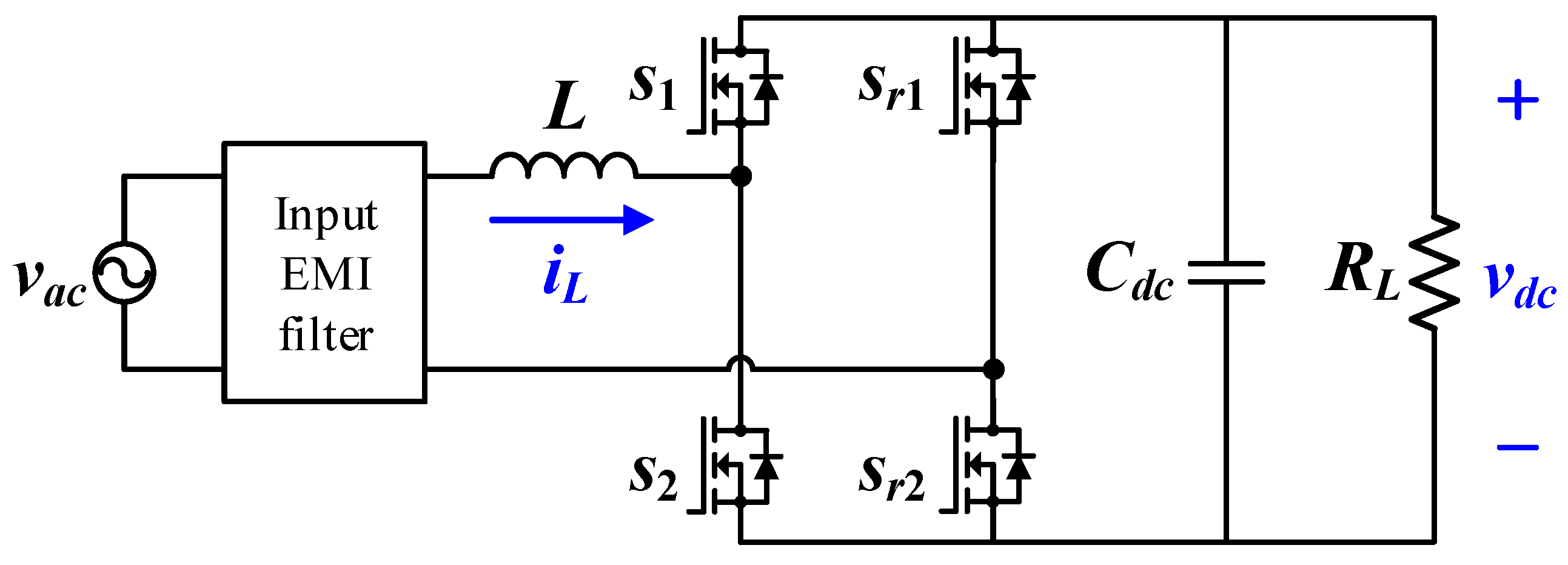
2. Operation Principle of TBPFC

Figure 1 is a circuit diagram of TBPFC. Here, vac, iL, vdc, L, Cdc, and RL mean grid voltage, inductor current, DC-link voltage, inductor, DC-link capacitor, and equivalent load resistance, respectively. Like a typical single-phase PFC circuit, an EMI filter removes high-frequency noise at the input stage. s1 and s2 are switches that operate at high switching frequencies and operate complementarily. sr1 and sr2 are rectifier switches that operate at a low switching frequency equal to the grid voltage frequency.
The current conduction path for each switching operation of TBPFC is shown in Figure 2. Figure 2a,b show the situation when vac is in a positive cycle with a positive voltage value. In this case, sr1 must be fully turn-off, and sr2 must be fully turn-on for rectifying operation. Figure 2a shows an operation mode where s1 is turned on. In a rectifying situation where power is supplied from the AC side to the DC side, the current flow is like an arrow direction as presented and, accordingly, the inductor voltage (vL) has a negative value, and the slope of iL has a (−) value. The rectified current charges the DC-link capacitor and supplies power to the load. Figure 2b shows the situation where s2 is turned on. Likewise, sr2 is turned on, and as s2 turns on, vL has a positive value, so the slope of iL becomes a (+) value. In this mode, the DC-link capacitor is discharged and supplies current to the load.
Figure 2c,d show situations when vac is in a negative cycle with negative voltage value, sr1 is fully turned on, and sr2 is fully turned off for the rectifying operation. Figure 2c shows an operation mode where s1 turns on, vL has a negative value, and the slope of the iL has a (−) value. As in Figure 2b, the DC-link capacitor is discharged and supplies current to the load. Figure 2d shows a situation where s2 is turned on and, accordingly, vL has a positive value, and the slope of iL has a (+) value. As in Figure 2a, the rectified current charges the DC-link capacitor and supplies current to the load.
A simple expression of the TBPFC according to the polarity of vac is shown in Figure 3. In the positive cycle corresponding to Figure 2a,b, s2 has the same role as the main switch of a general bidirectional boost converter, as shown in Figure 3a. When the duty ratio of the switch is D, the voltage transfer ratio M(D) and D can be expressed as Equations (1) and (2).
M ( D ) = V o u t V i n = v d c v a c = 1 1 D
D = 1 v a c v d c .
Here, Vin is the input voltage and is equal to vac, and Vout is the output voltage and is equal to vdc. The switching operation of s2 in the positive cycle should be the same as Equation (2).
On the contrary, in the negative cycle corresponding to Figure 2c,d, s1 has the same role as the main switch of the bidirectional boost converter, as shown in Figure 3b. Therefore, in the negative cycle, s2 must operate with a complementary duty ratio ( D ¯ ), as shown below:
M ( D ) = V o u t V i n = v d c ( v a c ) = 1 1 D
D = 1 + v a c v d c
D ¯ = 1 D = v a c v d c .
When a cycle changes from negative to positive, the duty ratio applied to s2 should suddenly change from 0 to 1. Likewise, the duty ratio must change rapidly from 1 to 0 when changing from a positive to a negative cycle. According to the characteristics of these switching operations, switching operations and control sequences of TBPFC should be appropriately implemented for the rectification point when the polarity of the AC voltage changes.

3. Proposed Control Algorithm

The overall control block diagram of the TBPFC proposed in this paper is shown in Figure 4. First, continuous conduction mode (CCM) control is performed through a PI-based double-loop controller to control the DC-link voltage and inductor current. And the d-axis voltage (vd) and q-axis voltage (vq) are calculated from the grid voltage through alpha-beta to the DQ transformation. A general single-phase PLL is used to extract the phase information of the grid voltage. Finally, a rectifying switch algorithm is applied to minimize the zero-crossing current spike problem. Details for each control algorithm are as follows.

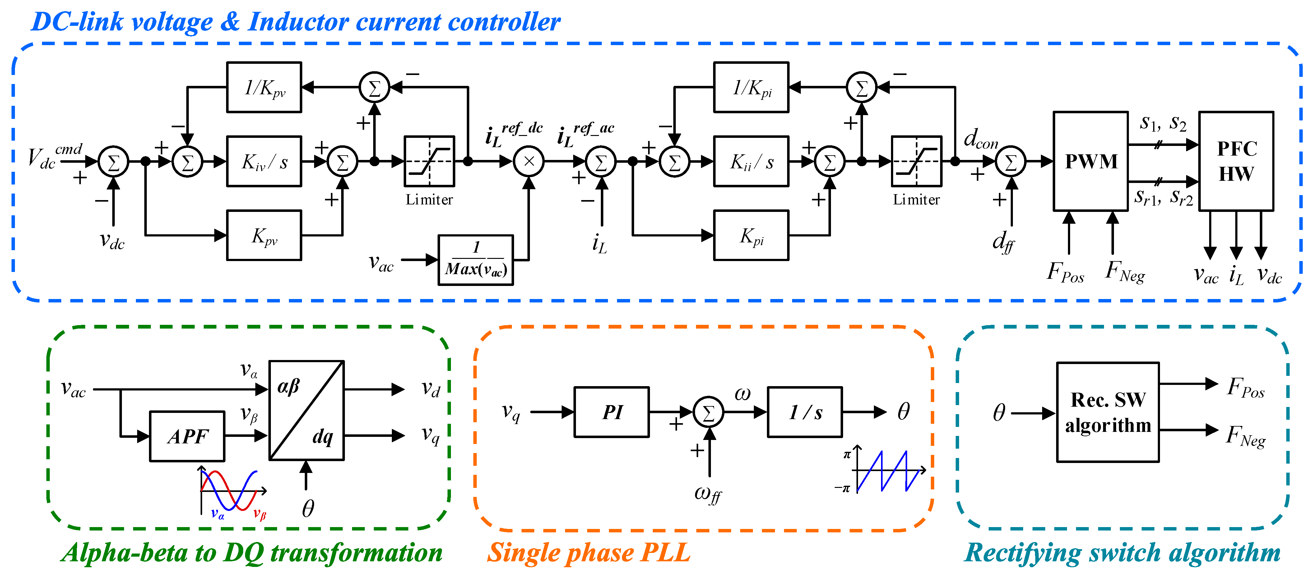
3.1. Digitalized Double Loop Controller

A double-loop control structure based on PI control is applied to simultaneously perform DC-link voltage control and power factor control on the AC input side. This control structure is implemented by a digitalized control environment within a predefined sampling time (generally the same as the switching period) in a microprocessor such as a digital signal processor (DSP). For this purpose, the PI controller and the low-pass filter must be converted from the continuous-time domain to the discrete-time domain through methods such as bilinear and backward, and the converted formula is implemented in a programming language such as C language. As a result, the control structure in Figure 4 is calculated based on the sensed data acquired by an analog-to-digital converter (ADC) interface, and the duty ratio is converted into a final switching signal through pulse-width modulation (PWM) to operate the TBPFC hardware.
The outer-loop controller is a DC-link voltage controller that performs PI control for the error between the DC-link voltage command (Vdccmd) and vdc. Kiv and Kpv refer to the I gain and P gain of the voltage controller, respectively. A limiter and an anti-windup control structure are applied to avoid excessive accumulation of error in the integral term. The output of the DC-link voltage controller is the inductor current reference, which means the maximum value of the inductor current to be controlled. Therefore, the DC reference value (iLref_dc) must be converted to the AC reference value (iLref_ac). Additionally, to maintain the power factor as an almost unity value, the phase of vac must be reflected in iLref_ac, which is expressed in Equation (4).
i L r e f _ A C = i L r e f _ D C v a c M a x ( v a c ) .
Here, Max(vac) means the maximum value of vac. The proposed algorithm uses the periodic average of the vd[n] (sampled value of vd) to minimize unnecessary fluctuations due to disturbances such as sensing noise in calculating Max(vac), as shown below.
M a x ( v a c ) = 1 N n = 1 N v d [ n ] .
Here, N is the number of data for periodic average calculation and, in this paper, the sampling frequency is set to 10 kHz, and N is set to 10,000 to reflect the Max(vac) value every one second.
The inner-loop controller is an inductor current controller that performs PI control for the errors of iLref_ac and iL. Kii, and Kpi refer to the I gain and P gain of the current controller, respectively. Due to the topological characteristics of TBPFC, the duty ratio must change suddenly at the zero-crossing point of vac, and this change is challenging to handle with the output of the PI controller. Therefore, the feed-forward duty ratio (dff), as shown in Equation (6), is added to the output of the current controller (dcon) to perform stable control.
d f f = { 1 v a c v d c    ,    P o s i t i v e    c y c l e    o f    v a c v a c v d c       ,    N e g a t i v e    c y c l e    o f    v a c .
The relationship in Equation (6) is the same as that derived in Equations (2) and (3). The final duty ratio is output as s1 and s2 through PWM, and sr1 and sr2 operate according to the positive flag (FPos) and negative flag (FNeg) of the rectifying switch algorithm, which will be described in Section 3.3.

3.2. Coordinate Transformation and PLL

The coordinate transformation used in the proposed algorithm is alpha-beta to DQ transformation, and vd is used to calculate the maximum value of the grid voltage shown in Equation (5). vq is used as an input variable of single-phase PLL. For coordinate transformation, an all-pass filter (APF) is used to make a 90° lagging voltage based on vac. The transfer function of APF, GAPF(s), is shown in Equation (7).
G A P F ( s ) = s + ω c s + ω c
ω c = 2 π f c .
Here, ωc and fc mean a cut-off angular frequency and a cut-off frequency, respectively, and fc is set equal to the frequency of the grid voltage (fac). The alpha-axis voltage (vα) is the same as vac, and the beta-axis voltage (vβ) is 90° lagging voltage through APF. The formulas for vd and vq calculated through coordinate transformation are as follows.
[ v d v q ] = [ cos θ sin θ sin θ cos θ ] [ v α v β ] .
In single-phase PLL, phase angle information is extracted using the vq value, and the angular frequency based on fac is added as a feed-forward term (ωff), as shown in Equation (10), assuming that the frequency variation of the grid voltage is slight.
ω f f = 2 π f a c .

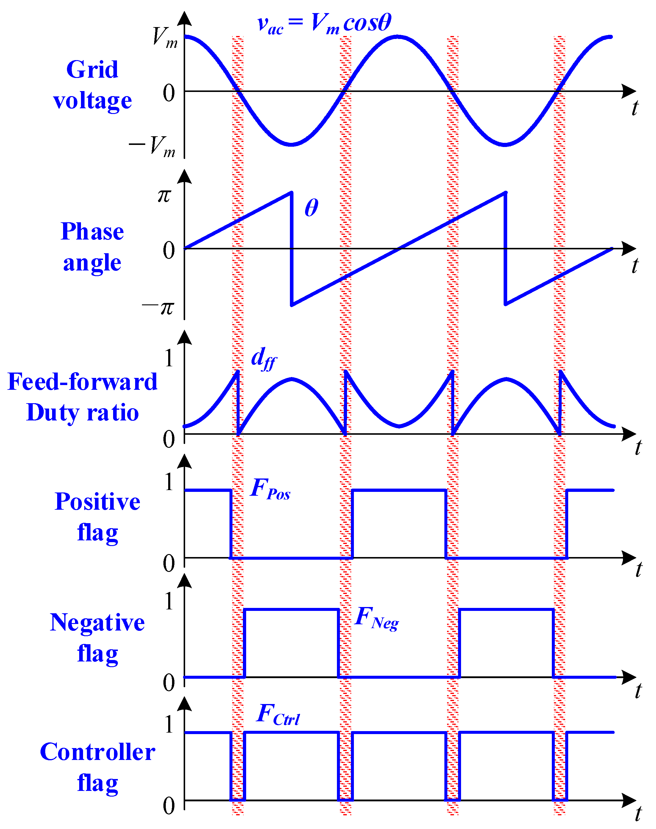
3.3. PLL Rectifying Switch Algorithm

The rectifier switch of TBPFC must be appropriately turned on and off according to the polarity of the grid voltage. The simplest way to implement an on/off sequence of rectifying switches is to use the sensed value of grid voltage directly. Although it has the advantage of being easy to implement, it may operate inappropriately due to a sensing noise. Accordingly, the rectifying switches may operate at an unwanted time, resulting in a zero-crossing spike current. As another method, a partial open-loop operation method is proposed. This method operates high-speed switches to a predefined duty ratio at rectification timing. This method requires initializing the closed-loop controller when operating the open-loop sequence, and there is a problem—that the transient response is repeated when the closed-loop control is reactivated. In addition, the complexity of the overall control sequence increases.
The rectifying switch algorithm proposed in this paper turns the rectifying switch on and off through the grid voltage phase angle (θ) extracted through the PLL. Basically, θ has a value from −π to +π and is a value that increases at every sampling time, so it is relatively robust to noise compared to conventional algorithms that directly use sensed values. In addition, because accurate judgment of the commutation point can be made through simple conditioning, false turn-on-off of the rectifying switch can be eliminated. And because there is no complicated switching sequence, it is easy to implement. The operating principle of the proposed rectifying switch algorithm is shown in Figure 5.
If the grid voltage is based on the cosine term, the θ value where a zero crossing of vac occurs is approximately 0.5π and −0.5π. Therefore, turn-off all switches before and after θ reaches 0.5π. Similarly, in the section before and after θ becomes −0.5π, all switches are equally turned off to prevent a zero-crossing spike current. The area where all switches turn off is the same as the red color section in Figure 5. At this time, the voltage-current controller also stops calculating to prevent unnecessary values from accumulating in the integral term and causing the output not to fluctuate significantly.
When the grid voltage is in a positive cycle, FPos is set to 1, and at this time, sr1 is turn-off, and sr2 is turn-on. Conversely, during a negative cycle, FNeg is set to 1; at this time, sr1 is turned on, and sr2 is turned off. The conditions for generating flag signals are as follows.
F P o s = 1     w h e n    ( π 2 + Δ θ )     θ     < ( π 2 Δ θ ) F N e g = 1     w h e n    θ ( π 2 + Δ θ )    o r    θ     < ( π 2 Δ θ )
Δ θ = 2 π f a c T s a m p N h y s
Here, ∆θ means the hysteresis band for phase angle, and Tsamp is the sampling period time. Nhys is a value that determines the width of the hysteresis band, and in this paper, Nhys is set to one to minimize the rectification area. In other words, since all switches turn- off only for two sampling times, a spike current does not occur, and a high power factor can be maintained due to the short rectification period. FCtrl is a flag signal for driving the voltage-current controller, and when FPos or FNeg is 1, FCtrl also becomes 1. There is no need to initialize the values in the digital controller because the calculations of controller are stopped for only a short period.

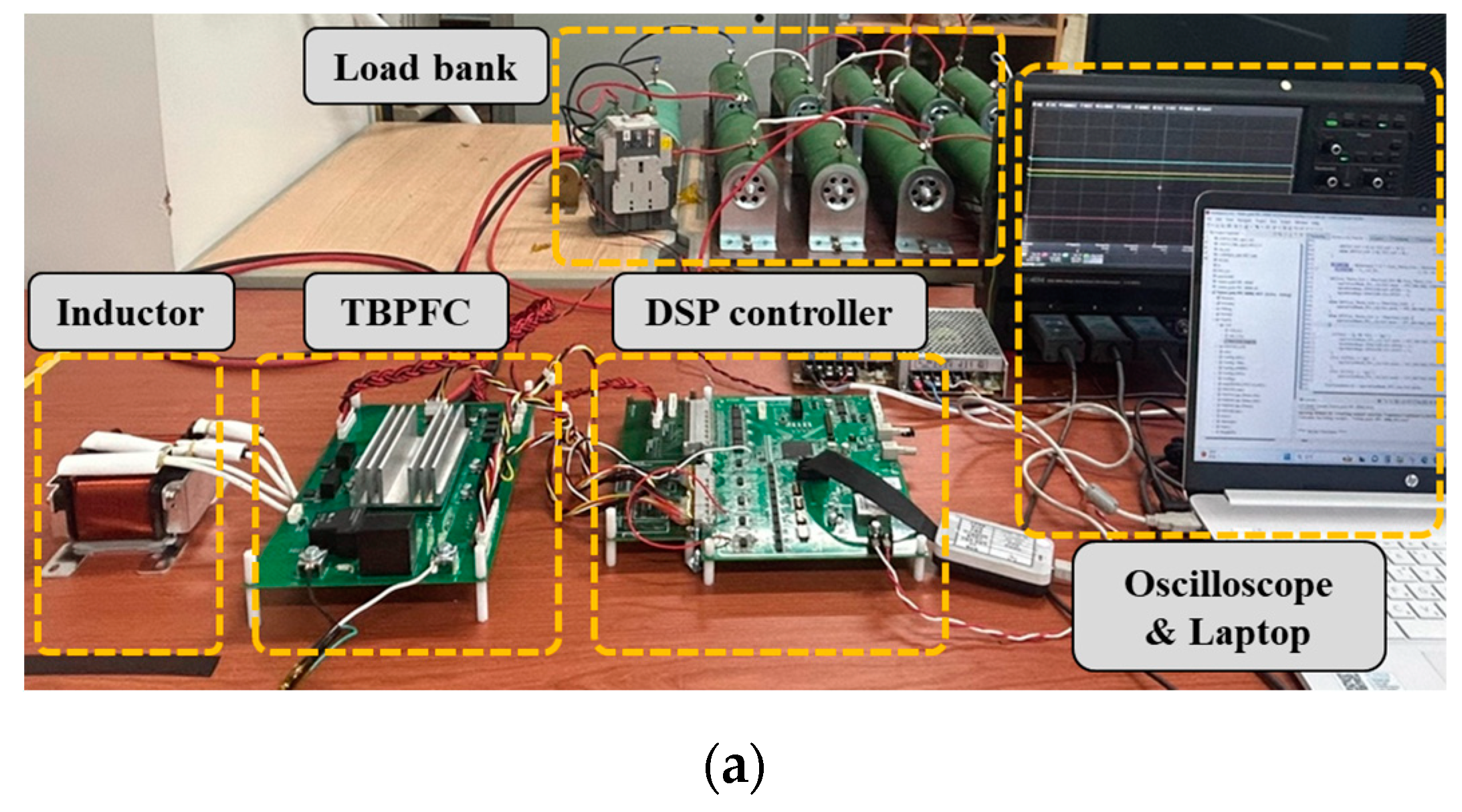
4. Realization and Experimental Results

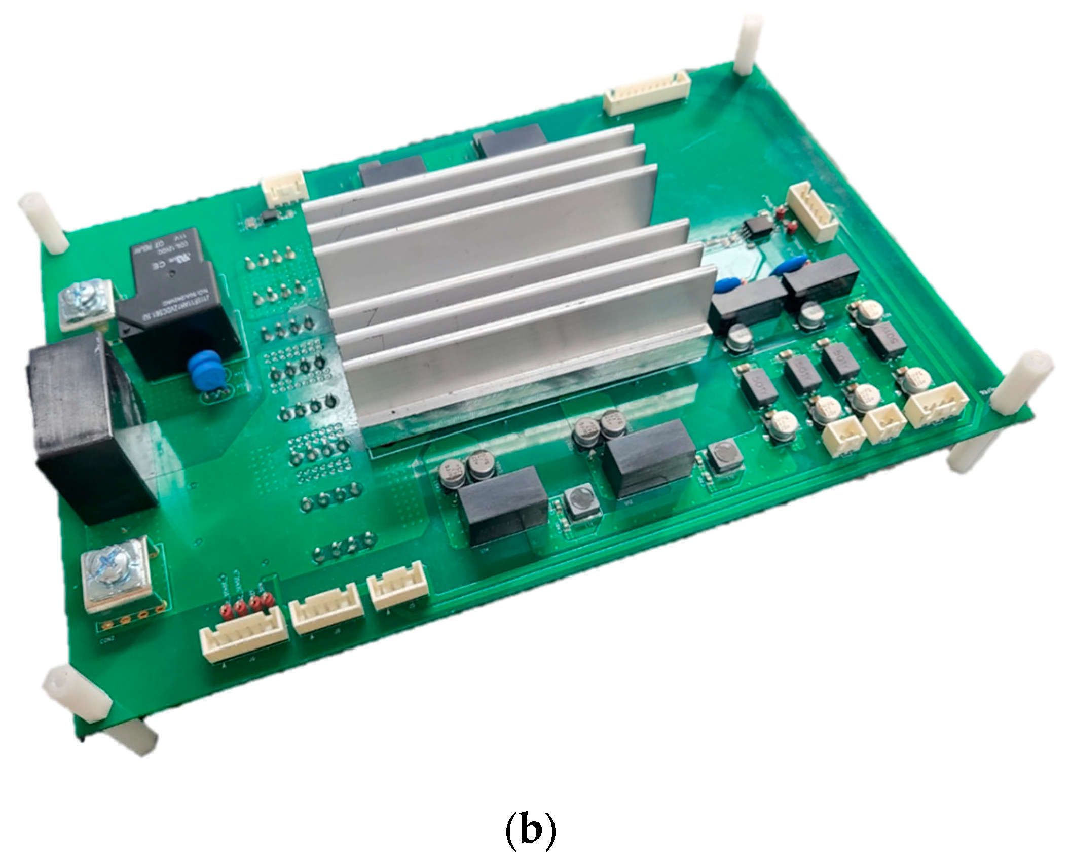
4.1. Hardware Specifications

A photograph of the prototype for verifying the proposed TBPFC control algorithm is shown in Figure 6. The input side consists of a relay and a thermistor to charge the initial DC-link voltage. The switch legs in Figure 1 are constructed using MOSFET switches and heatsink. Three sensors are used for DC-link voltage control and PFC control: input voltage, inductor current, and DC-link voltage. A control board based on TI’s DSP (TMS320F28377D) is used to implement the proposed algorithm. The detailed design specifications of the hardware prototype are listed in Table 1. The gains of the PI controller are shown in Table 2.

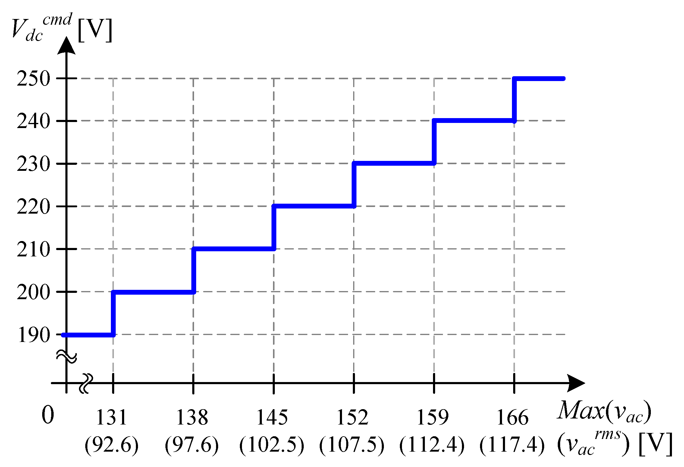
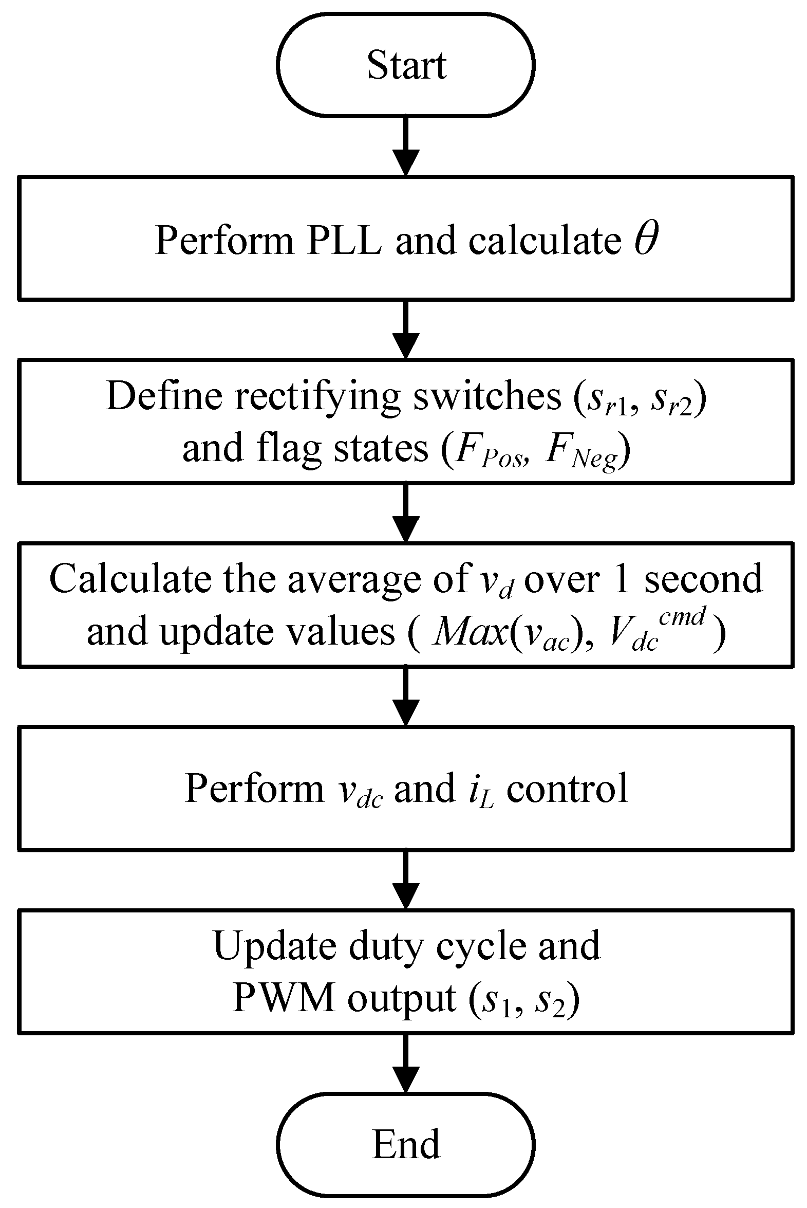
4.2. Algorithm Implementation

Figure 7 shows a graph of the DC-link voltage profile that varies depending on the magnitude of the input grid voltage. TBPFC is a boost PFC, so it is possible to boost the output voltage compared to the input voltage. In this paper, we verify the variation and control of the output voltage by implementing a sequence that allows the DC-link voltage to be varied according to input conditions without additional firmware modification. Based on the input voltage, it is divided into sections at approximately five Vrms intervals from 90 Vrms to 120 Vrms, and the corresponding DC-link voltage is defined to vary from 190 V to 250 V at 10 V intervals.
Figure 8 shows a flow chart of the entire controller sequence of TBPFC, including the rectifying switch algorithm. First, PLL is performed based on the sensing information, and the phase angle is calculated. Based on the phase angle, rectifying switches and flag states are predefined before activating the closed-loop controller. When the switching starts operating from the turn-off to the switching state after passing the rectification area, the switching status of sr1 and sr2 must be predefined before s1 and s2 operate, thereby preventing zero-crossing spike currents. In this paper, for sr1 and sr2 switching, the DSP peripheral is set to GPIO rather than PWM settings to activate immediately during control operations without on-off delay. Next, calculate the periodic average value of the vd and calculate Max(vac) shown in Equation (5). Additionally, as defined in Figure 7, the Vdccmd is determined according to vac. Likewise, to prevent unnecessary changes in DC-link voltage, a calculation sequence of Vdccmd is performed every one second. Next, DC-link voltage control is performed according to the defined Vdccmd, and inductor current control is performed according to the output current command of the voltage controller. Finally, the final duty ratio with the feed-forward term is calculated, and the switching status of s1 and s2 is determined through PWM.

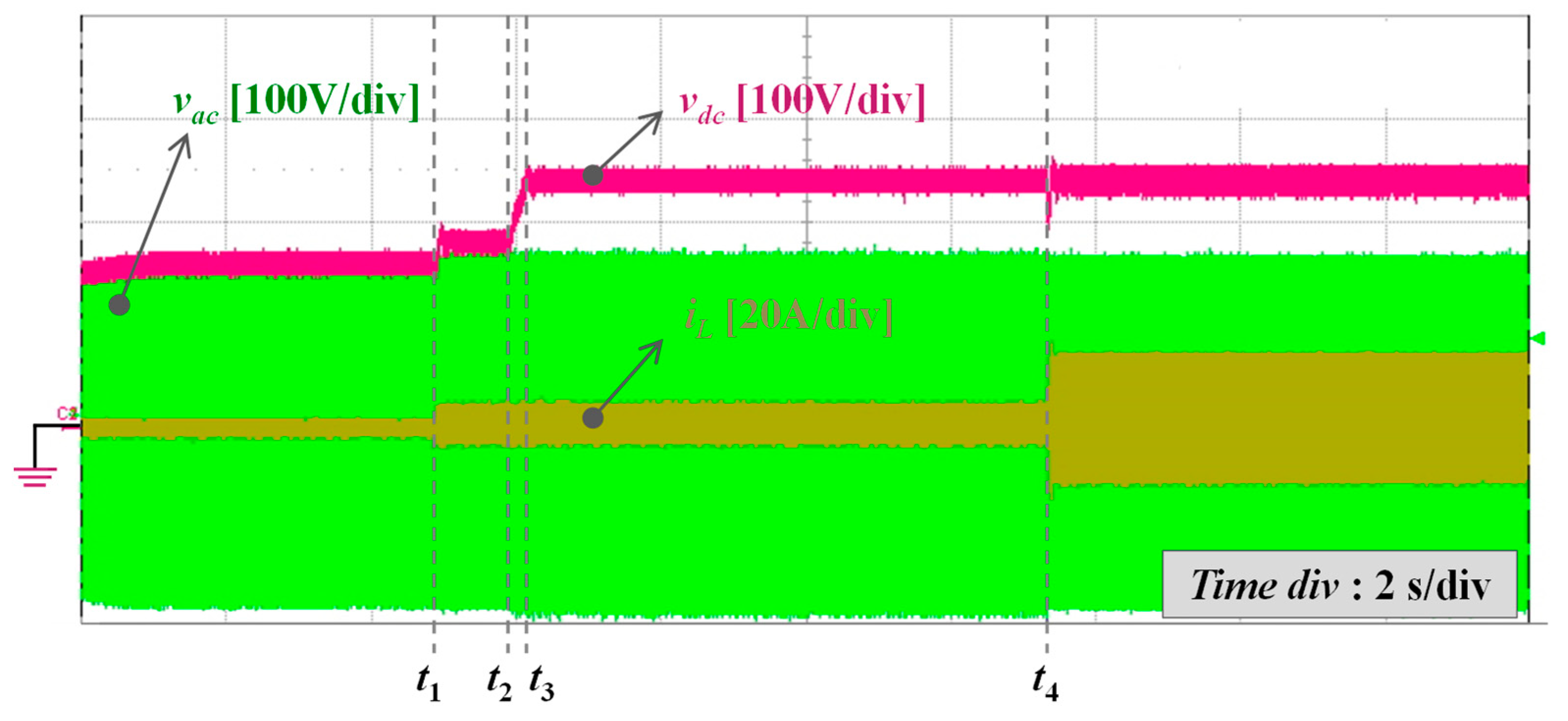
4.3. Experimental Results

Figure 9 shows the initial start-up sequence to which the proposed algorithm is applied. First, before t1, the DC-link voltage is charged through the initial charging resistance and relay, and the control algorithm is not applied. Afterward, control begins at t, and to prevent an excessive initial rise in DC-link voltage, Vdccmd is set to increase only +20 V to the voltage before applying control. The sequence shown in Figure 8 is then used to increase Vdccmd from t2 to t3. At this time, Vdccmd value follows the voltage profile shown in Figure 7. Additionally, to prevent a sudden increase in the Vdccmd value, a ramp-up function is used to output the command value. Through this, it takes a certain amount of time from t2 to t3 to reach the final command value, but excessive overshoot of voltage or current can be prevented.
Next, t3 to t4 show the operating waveform in a no-load situation. Although there is no load on the output, the inductor current has a ripple component due to the voltage difference between the input and output. At t4, the output load increases to about 600 W, and the inductor current increases accordingly. Through this, it can be confirmed that the initial no-load control is smoothly performed and adequately controlled without a sizeable transient state when the load suddenly changes.
Figure 10 shows the experimental results applying the proposed TBPFC control algorithm. The experiment is performed according to the input and output voltage conditions shown in Table 1 and Figure 7, and vac, iL, and vdc waveforms are measured at the maximum load of 3 kW. Figure 10a shows the situation when the minimum input voltage (90 Vrms) is applied. Vdccmd at this time is 190 V, and it can be confirmed that DC-link voltage control is performed according to the command. Likewise, Figure 10b,c show situations when the input voltage is 100 Vrms and 110 Vrms, respectively, and it can be seen that DC-link voltage control is properly performed depending on the input voltage conditions. Figure 10d shows the situation when the maximum input voltage (120 Vrms) is applied and, at this time, Vdccmd is 250 V, so DC-link voltage control is properly performed. Due to the topology characteristics of single-phase PFC, a ripple component of 120 Hz is inevitably present in the DC-link voltage, so it can be confirmed that low-frequency voltage ripple exists in all waveforms. However, it can be confirmed through the waveform that the low-frequency voltage ripple does not affect current control.
From Figure 10, it can be seen that, when the input voltage is gradually increased under the equal load conditions, the inductor current gradually decreases. Additionally, it can be confirmed that iL has the same phase as vac for all operating situations and that appropriate power factor control is performed. In addition, it can be confirmed that zero-crossing current spike does not occur in all experimental conditions, which proves the validity of the proposed rectifying switch algorithm.

5. Future Considerations

In this paper, a general single-phase PLL was used to calculate the phase angle. However, in environments where the frequency variation range is significant due to a weak grid or the size of the grid voltage varies frequently, advanced PLL techniques must be applied to extract appropriate phase angle information, even under adverse conditions. In the future, we plan to use advanced PLL methods to enhance the performance of the proposed algorithm. Additionally, if the capacitance of the DC-link capacitor reduced, the 120 Hz voltage ripple component increases, and PFC control performance may also be reduced accordingly. We plan to incorporate research into the proposed method to improve the performance of DC-link voltage control.

6. Conclusions

This paper proposed a digitized control algorithm for TBPFC with a simple control structure. The proposed algorithm consisted of a PI-based voltage and current controller, coordinate transformation and PLL, and a rectifying switch algorithm. The phase angle information of the grid voltage was used to implement overall control sequences to prevent current spikes at zero crossing. In the voltage and current controller, a feedforward term of duty ratio was applied for stable power factor control. A predefined voltage profile was implemented to change the command of DC-link voltage according to grid voltage. The performance of the proposed control algorithm was verified through a 3 kW hardware prototype. From the results of the experiment, the accurate performance of DC-link voltage and power factor control was verified.

Author Contributions

Conceptualization, G.-Y.L. and R.-Y.K.; methodology, G.-Y.L.; software, G.-Y.L.; validation, G.-Y.L., H.-C.P. and M.-W.J.; formal analysis, H.-C.P.; investigation, M.-W.J.; resources, R.-Y.K.; data curation, G.-Y.L.; writing—original draft preparation, G.-Y.L. and M.-W.J.; writing—review and editing, G.-Y.L., H.-C.P. and R.-Y.K.; visualization, G.-Y.L.; supervision, R.-Y.K.; project administration, R.-Y.K.; funding acquisition, G.-Y.L. All authors have read and agreed to the published version of the manuscript.

Funding

This results was supported by “Regional Innovation Strategy (RIS)” through the Natinal Research Foundation of Korea (NRF) funded by the Ministry of Education (MOE) (No. 2021RIS-003).

Data Availability Statement

Not applicable.

Conflicts of Interest

The authors declare no conflict of interest.

References

  1. Lee, Y.-D.; Kim, C.-E.; Kim, D.-M.; Choi, S.-H.; Moon, G.-W. A New Bridgeless PFC Converter having Low Common-Mode Noise and High Efficiency for Server Power Application. In Proceedings of the 2019 10th International Conference on Power Electronics and ECCE Asia (ICPE 2019—ECCE Asia), Busan, Republic of Korea, 27–30 May 2019; pp. 1–6. [Google Scholar]
  2. Baek, J.; Kim, J.-K.; Lee, J.-B.; Park, M.-H.; Moon, G.-W. A New Standby Structure Integrated with Boost PFC Converter for Server Power Supply. IEEE Trans. Power Electron. 2019, 34, 5283–5293. [Google Scholar] [CrossRef]
  3. Patel, N.; Lopes, L.A.C.; Rathore, A.K. Analysis and Design of Soft-Switching Single-Stage Single-Phase PFC Converter for Bidirectional Plug-in EV Charger. In Proceedings of the 2022 IEEE Energy Conversion Congress and Exposition (ECCE), Detroit, MI, USA, 9–13 October 2022; pp. 1–7. [Google Scholar]
  4. Pandey, R.; Singh, B. Bridgeless PFC Converter Based EV Charger. In Proceedings of the 2020 IEEE International Conference on Computing, Power and Communication Technologies (GUCON), Greater Noida, India, 2–4 October 2020; pp. 290–295. [Google Scholar]
  5. Rajasekaran, S.; Suresh, S.; Karthikeyan, K.; Bhuvanesh, A. Implementation of an A-Source DC–DC Boost Combination Phase-Shifting Full-Bridge Converter for Electric Car Rapid Charging Applications. J. Electr. Eng. Technol. 2023, 18, 2871–2884. [Google Scholar] [CrossRef]
  6. Kumar, K.A.; Veeramallu, V.K.S.; Narasimharaju, B.L. Performance Analysis of Coupled Inductor Based Ripple Free Boost PFC AC-DC LED Driver. In Proceedings of the 2020 IEEE International Conference on Power Electronics, Drives and Energy Systems (PEDES), Jaipur, India, 16–19 December 2020; pp. 1–4. [Google Scholar]
  7. Jha, A.; Singh, B. A bridgeless boost PFC converter fed LED driver for high power factor and low THD. In Proceedings of the 2018 IEEMA Engineer Infinite Conference (eTechNxT), New Delhi, India, 13–14 March 2018; pp. 1–6. [Google Scholar]
  8. Ponce-Silva, M.; Salazar-Pérez, D.; Rodríguez-Benítez, O.M.; Vela-Valdés, L.G.; Claudio-Sánchez, A.; De León-Aldaco, S.E.; Cortés-García, C.; Saavedra-Benítez, Y.I.; Lozoya-Ponce, R.E.; Aquí-Tapia, J.A. Flyback Converter for Solid-State Lighting Applications with Partial Energy Processing. Electronics 2021, 10, 60. [Google Scholar] [CrossRef]
  9. IEC 61000-3-2, Part 3–2; Limits for Harmonic Current Emissions (Equipment Input Current ≤16A per Phase). IEC: Geneva, Switzerland, 2005.
  10. Lee, D.G.; Kim, R.Y. Control of Hybrid Active Power Filter to Reduce Harmonics of 3-Phase Cap-Less Inverter. J. Electr. Eng. Technol. 2023, 18, 261–270. [Google Scholar] [CrossRef]
  11. Park, J.W.; Le, T.-V.; Kang, F.-S.; Park, S.-J. Novel Current Slope Control in Dual-Active-Bridge Converter Using Periodic Filters and Direct Access Memory in DSP. J. Electr. Eng. Technol. 2023. [Google Scholar] [CrossRef]
  12. Lee, G.-Y.; Cho, M.-S.; Kim, R.-Y. Lumped Parameter Modeling Based Power Loop Analysis Technique of Power Circuit Board with Wide Conduction Area for WBG Semiconductors. Electronics 2021, 10, 1722. [Google Scholar] [CrossRef]
  13. Araumi, R.; Yamada, R.; Wada, K. Improvement of Characteristics in CRM-PFC Using a Control Method based on Switching Frequency Limitation. In Proceedings of the 2022 International Power Electronics Conference (IPEC-Himeji 2022-ECCE Asia), Himeji, Japan, 15–19 May 2022; pp. 2213–2218. [Google Scholar]
  14. Dacol, R.P.; Heerdt, J.A.; Waltrich, G. Non-Isolated High Current Battery Charger with PFC Semi-Bridgeless Rectifier. In Proceedings of the 2019 IEEE 15th Brazilian Power Electronics Conference and 5th IEEE Southern Power Electronics Conference (COBEP/SPEC), Santos, Brazil, 1–4 December 2019; pp. 1–6. [Google Scholar]
  15. Dong, S.; Yang, X.; Xu, Y.; Wei, J.; Wang, K. GaN-based Interleaved CRM Totem-pole PFC Rectifier with Variable-step Adaptive ZVS Control. In Proceedings of the 2022 IEEE International Power Electronics and Application Conference and Exposition (PEAC), Guangzhou, China, 4–7 November 2022; pp. 247–251. [Google Scholar]
  16. Fan, C.; Liu, F.; Zhao, S. Research on SiC-based Totem-pole Bridgeless PFC Converter and Control Strategy. In Proceedings of the 2023 6th International Conference on Energy, Electrical and Power Engineering (CEEPE), Guangzhou, China, 21–23 April 2023; pp. 654–659. [Google Scholar] [CrossRef]
  17. Kwak, B.; Kim, J. Digital Implementation Method for Synchronous PWM Control of GaN Transistor at Zero-Crossing of Totem-Pole PFC in Energy Storage Applications. Electronics 2021, 10, 30. [Google Scholar] [CrossRef]
  18. Lee, Y.-D.; Baek, J.; Moon, G.-W.; Kim, C.-E. A Reconfigurable Totem-pole PFC Rectifier with Light Load Optimization Control Strategy and Soft-Switching Capability. IEEE Trans. Power Electron. 2021, 36, 4371–4382. [Google Scholar] [CrossRef]
  19. Naraharisetti, K.; Channegowda, J.; Green, P.B. Design and modeling of CCM average current control PFC AC-DC Boost converter. In Proceedings of the 2021 IEEE Green Technologies Conference (GreenTech), Denver, CO, USA, 7–9 April 2021; pp. 403–408. [Google Scholar]
  20. Gandhi, B.; Ezhilmaran, M. Achieving high input power factor for DCM boost PFC converters by controlling variable duty cycle. In Proceedings of the 2013 International Conference on Computation of Power, Energy, Information and Communication (ICCPEIC), Chennai, India, 17–18 April 2013; pp. 18–20. [Google Scholar]
  21. Chen, X.; Son, G.; Jin, F.; Li, Q. A Microcontroller-Based High Efficiency Critical Conduction Mode Control for GaN-Based Totem-Pole PFC. In Proceedings of the 2021 IEEE 22nd Workshop on Control and Modelling of Power Electronics (COMPEL), Cartagena, Colombia, 2–5 November 2021; pp. 1–7. [Google Scholar]
  22. El Aroudi, A.; Haroun, R.; Cid-Pastor, A.; Martinez-Salamero, L. Suppression of Line Frequency Instabilities in PFC AC-DC Power Supplies by Feedback Notch Filtering the Pre-Regulator Output Voltage. IEEE Trans. Circuits Syst. I Regul. Pap. 2013, 60, 796–809. [Google Scholar] [CrossRef]
  23. Rao, V.M.; Jain, A.K.; Reddy, K.K.; Behal, A. Experimental Comparison of Digital Implementations of Single-Phase PFC Controllers. IEEE Trans. Ind. Electron. 2008, 55, 67–78. [Google Scholar] [CrossRef]
  24. Cabezas, J.J.; González-Medina, R.; Figueres, E.; Garcerá, G. Comparison and combination of digital controls for single-phase boost PFC converters in avionic power systems. In Proceedings of the 2017 IEEE 26th International Symposium on Industrial Electronics (ISIE), Edinburgh, UK, 19–21 June 2017; pp. 645–650. [Google Scholar]
  25. Sun, B. How to reduce current spikes at AC zero-crossing for totem-pole PFC. Analog. Appl. J. 2015. Available online: https://www.ti.com/lit/slyt650 (accessed on 1 September 2023).
  26. Sun, B. Control challenges in a totem-pole PFC. Analog. Appl. J. 2017. Available online: https://www.ti.com/lit/pdf/slyt718 (accessed on 1 June 2023).
  27. Gong, X.; Wang, G.; Bhardwaj, M. 6.6kW Three-Phase Interleaved Totem Pole PFC Design with 98.9% Peak Efficiency for HEV/EV Onboard Charger. In Proceedings of the 2019 IEEE Applied Power Electronics Conference and Exposition (APEC), Anaheim, CA, USA, 17–21 March 2019; pp. 2029–2034. [Google Scholar]
  28. Koh, H.-G.; Ko, H.-J.; Choi, Y.-J. A MPCC-Based Variable Sampling Time Interleaving Method for a Two-Phase Totem-Pole Bridgeless Boost PFC Converter. IEEE Access 2023, 11, 104295–104304. [Google Scholar]
  29. Lee, J.-Y.; Chen, J.-H.; Lo, K.-Y. Design of a GaN Totem-Pole PFC Converter Using DC-Link Voltage Control Strategy for Data Center Applications. IEEE Access 2022, 10, 50278–50287. [Google Scholar]
Figure 1. Circuit diagram of TBPFC.
Electronics 12 04449 g001
Figure 2. Operation mode of TBPFC: (a) vac positive cycle with s1 turn-on; (b) vac positive cycle with s2 turn-on; (c) vac negative cycle with s1 turn-on; (d) vac negative cycle with s2 turn-on.
Electronics 12 04449 g002
Figure 3. Simplification of TBPFC according to the polarity of input voltage: (a) At positive cycle; (b) At negative cycle.
Electronics 12 04449 g003
Figure 4. Overall control block diagram of TBPFC.
Electronics 12 04449 g004
Figure 5. Operation waveform of proposed rectifying switch algorithm.
Electronics 12 04449 g005
Figure 6. Photographs of the experimental environment: (a) Overall experimental setup; (b) hardware photograph of TBPFC prototype.
Electronics 12 04449 g006aElectronics 12 04449 g006b
Figure 7. Profile of DC-link voltage variation.
Electronics 12 04449 g007
Figure 8. Overall flow chart of proposed TBPFC control algorithm.
Electronics 12 04449 g008
Figure 9. Experimental waveform during the start-up sequence.
Electronics 12 04449 g009
Figure 10. Experimental waveform at 3 kW full-load: (a) vac = 90 Vrms, vdc = 190 V; (b) vac = 100 Vrms, vdc = 210 V; (c) vac = 110 Vrms, vdc = 230 V; (d) vac = 120 Vrms, vdc = 250 V.
Electronics 12 04449 g010
Table 1. Hardware specification of TBPFC.
ParametersSymbolValues
Rated powerP3 kW
Input grid voltage vac90~120 Vrms
Output voltage vdc190~250 V
Inductance L1.3 mH
Capacitance C1.05 mF
Switching frequency fsw10 kHz
Sampling time Tsamp100 μs
Table 2. PI gains of proposed algorithm.
ParametersSymbolValues
P gain of voltage controllerKpv0.08
I gain of voltage controllerKiv10.0
P gain of current controllerKpi0.02
I gain of current controllerKii5.0
Disclaimer/Publisher’s Note: The statements, opinions and data contained in all publications are solely those of the individual author(s) and contributor(s) and not of MDPI and/or the editor(s). MDPI and/or the editor(s) disclaim responsibility for any injury to people or property resulting from any ideas, methods, instructions or products referred to in the content.

