1. Introduction
Electronic devices have permeated nearly every facet of our lives, enabling convenience, efficiency and connectivity previously unimaginable. These devices encompass a broad spectrum, ranging from consumer electronics like smartphones and laptops to critical infrastructure [
1] components in healthcare, energy and transportation systems. However, as our reliance on these devices grows, so does the imperative of securing them against an array of threats, both digital and physical. In the realm of electronic device security, the focus extends beyond safeguarding data and digital assets; it also encompasses the physical security of these devices [
2]. Physical security plays an equally crucial role in ensuring the overall integrity of electronic systems, as unauthorized physical access can be as damaging as cyberattacks [
3]. From protecting sensitive hardware components to preventing tampering and theft, robust physical security measures are essential to maintain the reliability and functionality of electronic devices [
4].
Security threats come in various forms, with invasive and side-channel attacks representing the two most prominent categories. Invasive attacks involve physical tampering with the device, where adversaries gain unauthorized access to its internal components. Such attacks often include the insertion of hardware trojans or counterfeit components, potentially compromising the device’s functionality and security. On the other hand, side-channel attacks exploit unintentional information leaks during the device’s operation. These attacks analyze physical characteristics like power consumption, electromagnetic emissions or execution time to extract sensitive information such as cryptographic keys. Both invasive and side-channel attacks pose significant challenges to electronic device security, highlighting the need for comprehensive countermeasures to protect against both digital and physical threats.
Each protection method has specificities depending on which aspect is being kept confidential [
5]. One scenario involves securing sensitive information on the hardware, whether a known or unknown implementation, where the attacker seeks to gain access to this information [
6]. The other scenario is where the attacker attempts reverse engineering to reconstruct the hardware and/or software without directly accessing the information on the targeted device. In both cases, the level of protection must be proportional to the value of the information. When protecting low-value information, the implemented hardware or software does not necessarily have to be complex or advanced [
7]. The fundamental rule is that the time or resources invested in acquiring the necessary information should not be justified by the value of the obtained data.
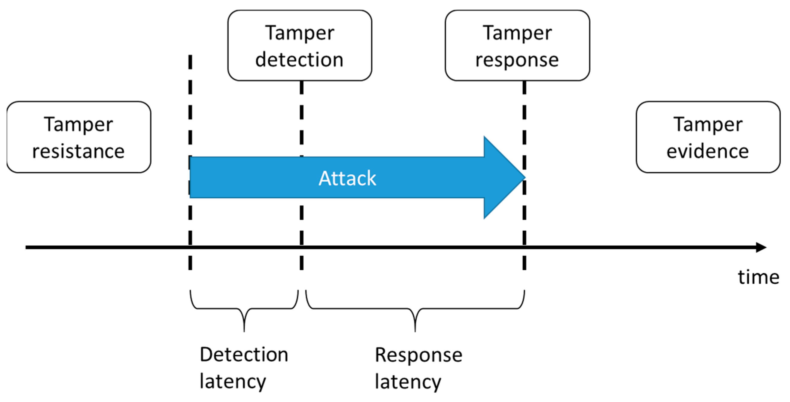
Protection against physical manipulation, or anti-tampering protection, is necessary for secure hardware [
8]. There are four levels of anti-tampering protection: tamper resistance, tamper evidence, tamper detection and tamper response. Tamper resistance signifies that the device incorporates a method or methods that make it challenging for an attacker to access the device’s internals. Tamper evidence is a technique that ensures any manipulation, such as opening the device’s casing, leaves visible proof. The technique itself does not prevent the attacker but merely provides evidence of manipulation. Tamper detection is a technique that ensures the device can detect attempted manipulation in real-time, achieved through the implementation of various sensors. The tamper response builds upon the tamper detection. The most common approach is that, once manipulation is detected, all confidential data on the device are erased. From the perspective of developing a mobile cryptographic device, it is advisable to implement all four anti-tampering techniques. In cases where selection is necessary, preference should be given to the combination of tamper detection and tamper response techniques.
In the contemporary world, electronic components are nearly ubiquitous in all aspects of daily life, including Internet of Things (IoT) systems [
9], industrial applications, military applications and more. Since most of these devices are based on microcontrollers, side-channel attacks emerge as a primary concern for hardware security. In the realm of cryptography, side-channel attacks are recognized as a threat to the security of computer and communication systems that seek to ensure the confidentiality and integrity of sensitive data. By analyzing information from physical side-channels such as power consumption, timing or electromagnetic emissions, even mathematically secure cryptographic algorithms can be effectively compromised. The relevance and necessity of hardware device protection [
10] are further underscored by standards that define required levels of physical protection for specific classes and types of devices. Some notable standards that encompass hardware protection include Common Criteria, TEMPEST, FIPS, IEEE and IEC CISPR, to name a few.
This work describes both invasive and non-invasive attacks, as well as methods to combat these attacks. It is essential to note that protection against non-invasive attacks begins during the device’s design and construction phase. Designers take specific measures to protect the device and prevent such attacks [
11]. This paper provides a comprehensive review of the scientific literature and patents describing hardware-based protection methods against invasive and non-invasive attacks.
Section 2 describes various types of invasive and non-invasive attack methods targeting electronic devices.
Section 3 and
Section 4 describe hardware-based protection methods against invasive and non-invasive attacks, respectively. In each section, a comparative analysis of listed methods is given. This paper concludes with a conclusion section and a list of references used.
2. Attack Types
Attack techniques are divided into categories according to the invasiveness they require. We distinguish between non-invasive and invasive attacks (
Figure 1). Non-invasive attacks are considered to be generally cheaper as they are based on the observation or manipulation of devices without physical damage. They require only moderately sophisticated equipment and knowledge to implement and execute the attack. Non-invasive attacks allow an attacker to monitor the analog characteristics of power connections, interfaces of any kind and the device’s electromagnetic radiation. With the help of these methods, it is possible to get to the information contained inside the device without physically disassembling it or leaving traces of unauthorized use.
Invasive attacks are considered more expensive to execute, but they have higher rewards for the attacker. Invasive attacks provide almost unlimited possibilities of extracting information and functionalities from devices. They require expensive equipment, knowledgeable attackers and sufficient time to execute the attack.
The simplest invasive attack type is micro-probing, which can be used to directly access the surface of the chip, so that the device can be observed, manipulated and disrupted. On devices that do not have physical protections implemented or are bypassed, it is possible to use microprobes to monitor data buses that should not be accessible to the user. Some of these buses may be unencrypted or contain raw data. In general, micro-probing allows for tapping signals inside the chip, injecting test signals and observing the reaction, which can be used to extract secret keys and memory contents. More complex invasive attacks require decapsulation of the device or integrated circuit. This can be achieved using laser etching to remove the polymer layer of the surface of the chip, to remove the passivating layer and to enable micro-probing attacks. Laser attacks can also be used to precisely cut metal traces inside the chip.
“Traditional” side-channel attacks, which involve monitoring power consumption or electromagnetic emissions, require an attacker to be in physical possession of the device to observe and analyze the leaked information. Still, different attacks assume different types of attackers and different levels of invasiveness [
12]. More specifically, in order to systematically analyze side-channel attacks, they are categorized into two orthogonal groups: passive vs. active and physical properties vs. logical properties.
Passive vs. active: This category distinguishes between attackers who passively observe side-channel information leaks and attackers who actively influence the target through any side-channel. For example, an attacker can manipulate a target, its input or its environment through any side-channel to subsequently observe information leakage through the target’s abnormal behavior or to bypass security mechanisms. The same division is proposed by the authors in the paper [
13].
Physical properties vs. logical properties: This category classifies side-channel attacks according to the information used, i.e., depending on whether the attack exploits physical properties (hardware) or logical properties (software features). Physical properties include power consumption, electromagnetic emissions or physical movements of the mobile communication device during operation. Logical properties include usage statistics provided by the operating system, such as data usage statistics or an application’s memory footprint. This work is based on protection against side-channel attacks through physical properties, i.e., hardware approach.
2.1. Passive Attacks
Power analysis: The power consumption of a device also depends on the data processed and the actions performed. Power analysis attacks exploit this information leakage to make inferences about sensitive information. As the name suggests, the power consumption, which is usually measured as the voltage drop across a resistor embedded in the power line, serves as a side-channel. State-of-the-art printed circuit board designs, including multi-layer constructions, as well as surface mount devices and packaging techniques (BGA—ball grid array), make it difficult to access a suitable feed line without permanent modifications. Depending on whether a single measuring line or multiple conductors are required, we distinguish between simple power analysis attacks and differential power analysis attacks [
13].
Exploiting information leaks (e.g., from software or hardware implementation of cryptographic modules) from side-channel attacks is an important challenge for designers and evaluators of such modules. When the cryptographic module performs encryption or decryption, secret keys can be discovered from side-channel information, such as runtime and power consumption. A typical example of a side-channel attack is a power analysis attack.
Electromagnetic analysis using EM fields generated by a cryptographic module has also been proposed as an extension of power analysis attacks [
14]. EM analysis attack is based on measuring and analyzing the device’s electromagnetic radiation. Multiple measurements and detailed analysis are often required to detect patterns in EM radiation. In the paper [
15], the authors demonstrated that it is possible to reconstruct an image from a laptop screen by measuring and analyzing the laptop’s EM radiation.
Therefore, PCB-level EM analysis also poses a significant threat to a cryptographic device (i.e., electrical devices containing cryptographic modules), even if the modules are equipped with conventional countermeasures against direct access and measurement of EM radiation, such as shielding. In the paper [
14], the authors present a practical example of a method for identifying critical parts associated with information leakage at the PCB level, which enables the design of effective EMC countermeasures to suppress information leakage.
EM side-channel attacks, although they do not require physical changes to the system being attacked and allow the attacker to select a location with maximum information leakage, introduce additional challenges compared to side-channel power analysis attacks. For example, as EM signals undergo a power-to-EM transformation that reduces the amplitude compared to measurement noise, this means that more measurements or more expensive measurement equipment will be required to perform an attack.
Given the limitations of current attack systems, the authors in the paper [
16] propose a low-cost, fully automated, end-to-end platform for performing effective EM side-channel attacks. The platform integrates EM scanning, measurement collection and attack/analysis in one step. Such an automated low-cost attack platform significantly increases the range of possible threats to IoT devices; however, it should be noted that the platform itself does not constitute a new attack, and existing countermeasures against EM side-channel attacks are effective against the presented platform.
2.2. Active Attacks
An active attacker manipulates a target, its input or its environment to subsequently observe information leakage through the target’s abnormal behavior or to bypass security mechanisms directly. While the transition between local and nearby attackers is seamless in passive attacks, active attacks always assume that the attacker is in possession of the device (at least temporarily).
Clock/Power Glitching: Variations in the clock signal, e.g., overclocking, have been shown to be an effective method of introducing errors into embedded devices. One of the prerequisites for this attack is an external clock source. Microcontrollers used in mobile communication devices usually have an internal clock generator, making tampering with the clock difficult. In addition to disrupting the clock, predicted power supply variations provide an additional method for introducing errors. With minor hardware modifications, power tampering can be implemented on most microcontroller platforms.
Electromagnetic Fault Injection (EMFI): Transistors placed on microchips can be affected by electromagnetic emissions, which is the basic assumption for this type of attack. EMFIs use short (in the nanosecond range) high-energy EM pulses to, for example, change the state of memory cells, resulting in erroneous calculations. Unlike voltage faults, where the injected fault is usually global, EMFI allows for targeting specific areas of the microchip by precisely placing the EM probe, e.g., in instruction memory, data memory or CPU registers. Compared to optical fault injection, EMFI attacks do not necessarily require chip unpacking, making them more practical.
Laser/Optical Faults: Laser beam optical attacks are among the most effective fault injection techniques. These attacks take advantage of the fact that a focused laser beam can change the state of a transistor on a microcontroller, resulting in, for example, flipping bits in memory cells. Compared to other fault injection techniques (e.g., EMFI), this method is more demanding. First, decapsulation of the chip is a prerequisite for accessing the silicon with a laser beam. Second, finding the correct spot for the laser beam is also not easy.
Temperature variation: Operating the device outside its specified temperature range may cause erratic behavior. Heating the device above the maximum specified temperature can cause errors in the memory cells. Cooling the device affects the rate at which RAM content disappears after shutdown (RAM remanence effect).
3. Methods of Protection against Invasive Attacks
The goal of anti-tampering mechanisms is to prevent any attempt by an attacker to perform an unauthorized physical or electronic action against the device. Anti-tampering techniques include tamper resistance, tamper detection, tamper response and tamper evidence (
Figure 2). Anti-tampering techniques are designed to make it difficult for an attacker to carry out and succeed in an attack. These techniques can include physical protection mechanisms (e.g., packaging) and the hardware design itself (e.g., implementing additional circuits). In case an attack is launched despite the prevention techniques used, tamper detection techniques try to detect the attack as soon as possible. The elapsed time interval between the initiation of an attack and its detection (detection latency) and the time interval between detection and response (response latency) represent the period of vulnerability and should be kept as low as possible.
Tamper resistance is the ability to resist unauthorized access attempts, i.e., to make access to the device difficult. It is most often used at the level of the device housing. The following can be used to create a protected housing: safety screws, adhesives, encapsulation and ultrasonic welding. Safety screws have specialized heads that cannot be opened with standard screwdrivers. They are only useful for low-motivation attackers. Adhesives are used to assemble the device and are released by applying heat. Ultrasonic welding is used to weld, for example, plastic casings to prevent opening and reduce the cost of production. Ultrasonic welding of the housing creates a housing that is effectively one piece of the material. It is difficult to open it without leaving traces of tampering. Encapsulation or coating (acrylic, epoxy or silicone) is used for protection from the elements (against dust, moisture, corrosion, etc.), tampering (modification of the circuit for functions that are not enabled at the factory), reverse engineering (to protect intellectual property) and cloning (for preventing counterfeit products from being placed on the market).
Tamper detection is the ability of the system to detect tampering. The goal of tamper detection mechanisms is to distinguish authorized use of the device from unauthorized use. The most common mechanisms used are tamper switches, tamper sensors and tamper circuits. Tamper switches are used to detect the opening of the device housing. When the cover is removed from the housing, the microswitch makes contact or breaks it, thus detecting the opening of the housing. They can be made with mechanical microswitches, magnetic switches and pressure contacts. Tamper sensors are used to detect parameter changes, so if any parameter is outside the circuit’s normal operating conditions, manipulation (accidental or intentional) is detected: temperature sensors that can detect changes in operating temperature (e.g., cold start attack); voltage sensors that can detect changes in operating voltage (e.g., glitch attacks); radiation sensors that can detect X-rays, ion beams and infrared radiation; capacitive or inductive sensors; resistive sensors; ultrasonic sensors; and optical sensors. Vibration sensors can detect mechanical attack attempts from grinding or drilling. Applying the same functionality using an accelerometer can make it significantly more difficult for an attacker to find and bypass the sensor. Light sensors such as photodiodes or photoresistors can detect the opening of the case through the presence of light inside the opaque case. Protective circuits (i.e., protective envelopes) are used to detect unauthorized access or make it difficult to create a functional circuit diagram. The most common examples of attack detection protection circuits are conductive networks wrapped around critical hardware circuits to detect attack attempts. At the ends of sensors of this type, some circuits can detect small changes in the sensor’s electrical properties or interruptions in optical fiber conduction. Protective envelopes belong to more advanced methods and are described in more detail in the rest of the chapter.
Tamper response is the device’s ability to react to detected tampering. Types of responses to detected unauthorized access are turning off or blocking the device, erasing critical parts of the memory or the entire memory, and physically destroying the device. Device blocking is an effective way to protect data. Erasing critical parts of memory (memory zeroization) includes erasing all key data that can be used for the future decryption of information or the information itself that is being protected. Physical destruction of the device is most often performed by significantly raising the supply voltage. This functionality is easy to implement with a boost converter on the power supply. A different method is to make a circuit or chip on a glass substrate. The base is fragile and sensitive to drops/vibrations or sudden changes in heat. It can be used for detection, response and proof of tampering.
Tamper evidence or tamper-proof is the ability of a device to retain evidence of tampering for a more extended time period. Examples of tamper-proof methods are the use of cases with tamper-evident labels or security locks, coatings or encapsulation materials that show traces of tools or other forms of tampering, and paint that contains bubbles of a different color (e.g., bleeding color). When the bubbles are broken, the colors are mixed and a third color is created that is easily visible. The scientific literature and published patents describing anti-tampering methods represent the following three areas: conductive meshes, sensors and PUF techniques. All three methods enable tamper detection, and depending on the type of manipulation, they can also provide tamper evidence.
3.1. Conductive Meshes
The anti-tampering technique using conductive meshes is based on armor around the protected assembly (or part of the assembly) on which a parameter change is easily detected (tamper-proof). Continuous measurement within the system detects tampering and can be used as a trigger to initiate a tamper response. In the paper [
17], a hardware design is proposed, i.e., a protective conductive mesh structure that can detect manipulation or changes on the PCB. The device does not use auxiliary power in the form of a battery. While the hardware is turned off, there is no protection, i.e., the mechanisms do not detect circuit manipulation. Security is achieved by initializing the device when it is turned on and monitoring the state of the hardware. Changes to the physical structure affect the generated cryptographic key. If the key does not match the factory key, tampering has been detected and the device reports an error. Any change in the structure of the protective mesh results in tamper detection.
The authors in [
18] describe hardware protection based on a conductive mesh. Manipulation of the conductive mesh must be detected during device initialization. Different responses of the conductive mesh made of thicknesses of 0.3 and 0.6 mm at different temperatures and frequencies were demonstrated. The paper [
18] presents a security solution for protecting small- and medium-sized electronic devices, such as IoT and IoE devices. The solution is based on a conductive mesh that is used to protect against unauthorized access or manipulation. An active tamper detection circuit examines the conductive mesh with signals and generates a cryptographic key. This key is used to decrypt the device’s software at device startup. If the conductive mesh properties are changed, the software will decrypt incorrectly. In this way, the software and the contained data are secured.
The work described in [
19] is based on hardware protection using a conductive mesh for tamper detection and PUF key generation. The dimension of the conductive mesh is designed to protect the device from drilling with mechanical drills larger than 300 µm in diameter. Two conducting meshes have a mutual property of capacitance and each an individual property of resistance or conductance. Replacing one conductive mesh with a resistor would satisfy the conductivity condition but degrade the capacitance. Another function of the metal mesh is to protect against external EM radiation and, at the same time, prevent the analysis of the EM spectrum using magnetic probes.
The capacity and conductivity of the protective layers are continuously monitored during device operation. The paper [
19] describes ways of compensating and calculating the capacity of the device due to differences in the assembly. The circuit for measuring system capacity is taken from the paper [
20]. Micro-probing enables data interception directly on the chip bus or individual transistors, as well as error injection. This is a common attack technique. For protection, an LAPD (Low-Area Probing Detector) can be used as an effective approach to detect micro-probing proposed in the paper [
21]. The detection technique boils down to comparing the delay difference between symmetrical lines, such as bus lines, to detect the timing asymmetry introduced by the capacitive load of the probe.
Probing detection is based on measuring the delay between two digital signals caused by the capacitive loading of one line by a microprobe. In case the line capacity of the device is significantly higher than the capacity of the microprobe, the detection would not be successful. The detection accuracy of the LAPD assembly depends on the capacity of the microprobe. The higher the probe capacity, the greater the chance that the attempt will be detected. Conductive mesh protection methods are the most commonly used methods among published patents. Patents with different methods based on conductive meshes are described below.
Patent “Mobile terminal provided with security function” [
22] describes a method of tamper detection by measuring the change in resistance of a conductive rubber (due to a change in pressure) that is placed between two parts of the device housing. The resistance of the rubber is changed by changing the pressure on the rubber, which is a consequence of the closing of the upper and lower halves of the housing of the protected device. By opening the housing, the pressure on the conductive rubber changes and the opening is detected by this mechanism. The proposed innovative concept applies to mobile communication terminals, payment terminals and various computers and tablet PCs, particularly to the payment terminal industry.
Patent “Tamper detection” [
23] describes the method of detecting manipulation by measuring the change in resistance of the conductive mesh that covers sensitive hardware. A random signal (that cannot be externally replicated and bypassed) is transmitted through the conductive mesh. If the transmitted signal at one end of the conductive mesh does not reach the receiver, damage to the conductive mesh is detected. After that, the processor decides the system’s reaction to the detected manipulation. If the module detects tampering, it is configured to clear the memory immediately, even if the rest of the system is disabled or destroyed. The invention can also detect attacks with a high-frequency EM signal. An attack is detected if the transmitted signal reaches the receiver too quickly.
Patent “Tamper Detection Techniques” [
24] describes a tamper detection method by measuring the change in resistance difference of a conductive mesh. Each conductive mesh represents the resistance with which the resistive divider is formed, and reference voltage values are compared with those obtained on the resistive divider of the conductive meshes. In addition to cutting conductive networks, detecting the conductivity difference between two conductive meshes can be implemented. In this way, the detection threshold’s sensitivity increases and the protection level rises to a higher level. With the described methods, it is possible to detect damage to the conductive meshes, the cutting of each conductive network, the short-circuiting of conductive mesh lines or the mutual connection of two branches of conductive meshes. A comparison of changes in the conductive meshes is performed using operational amplifiers and/or voltage comparators with multiple inputs.
The patent “Tamper detector with hardware-based random number generator” [
25] describes a method of detecting manipulation by measuring the change in signal delay through a conductive mesh. The signal generated by the random number generator is sent through the conductive mesh and arrives at the other end if the mesh is not interrupted. Implementing linear feedback shift registers (LFSRs) to generate a pseudo-random coded signal is also proposed to achieve a higher protection level. A hardware-based random number generator generates random seed values directly loaded into the LFSR from the hardware random number generator. Therefore, random initial values are loaded into the LFSR without software interaction and without software visibility. The received input signal (which passes through the conductive mesh) is processed and compared with the original transmitted signal. Interruption of the conductive mesh or any other manipulation that causes variations in the transmitted signal triggers the protection mechanisms of the device.
The patent “Anti-tamper system” [
26] describes an anti-tamper system that uses a universal anti-tamper housing design. The presented invention relates to a system with anti-tamper properties and a modular, functionally isolated architecture. The device is configured to trigger a reset after tampering. The universal housing can be configured to allow the replacement of the information processing module or the cryptographic module without resetting the system after receiving and authenticating the message. The presented invention further provides an anti-tampering system configured so that its design can be reused in connection with different information processing modules or cryptographic modules.
Patent “Tamper-respondent assembly with interconnect characteristic (s) obscuring circuit layout” [
27] describes a method to protect against reverse engineering. The invention describes techniques for hiding conductive mesh interconnections. The patent includes multiple protections for proprietary information but concentrates on protection against reverse engineering. The protection is performed by making it difficult to reverse-engineer the connection scheme of the conductive network by making it difficult to detect the lines recorded by the X-ray device. Conductive lines can be formed of conductive material that can be detected using X-rays, which, combined with X-ray invisible interconnect material, makes the interconnections between layers of the printed circuit board, and thus the circuit layout, difficult to determine. In addition, it is possible to make fake interconnections visible through X-ray analysis, but which do not create a conductive connection between the layers.
The patent “Secure electronic circuitry with tamper detection” [
28] describes a tamper detection method by integrating conductive meshes into the device housing. The patent describes a method of protecting elements enclosed in a security enclosure that includes conductive meshes as protection against unauthorized openings that extend along its inner surface and are part of the enclosure and circuit to detect unauthorized access. The tamper detection circuit also detects tampering by monitoring the voltages at the reference points. The on-board part of the tamper detection circuit is connected to the conductive meshes via multiple connector parts. When tampering is detected, it can be localized based on voltages measured at multiple indentations along the chassis. The tamper detection circuit can be arranged in a Wheatstone bridge for better tolerance. The intrusion detection circuit can detect if the current stops flowing through one or more lines of conductive networks or if a short circuit occurs between the lines, which are the most common changes that occur if a malicious party intrudes the security enclosure by drilling, attempting to divert current within the tamper detection circuit, or by dousing part of the tamper detection circuit with conductive ink.
The patent “Enclosure to board interface with tamper-detect circuit” [
29] describes a tamper detection method to protect against the opening of the enclosure using glued lines of conductive meshes. The patent describes the method of creating conductive mesh lines so that they are sensitive and easily damaged by the application of a small force. The traces are made on the surface of the printed circuit board (upper or lower) in wavy shapes that cover a specific zone to which the cover or case of the protected assembly is glued. When attempting to remove the covers, the adhesive holding the cover secured to the chassis separates the conductive mesh from the printed circuit board and breaks the electrical connection of the conductive network.
3.2. Sensors
In addition to the classic approach of using additional sensors that can detect changes in environmental parameters to detect manipulation, consumption sensors can also be used to detect hardware trojans (HT). The trend of outsourcing hardware production to third parties increases the possibilities of malicious activities and consequently the security risk for hardware systems. Damage to the system can be caused by destructive modifications and spy versions called hardware trojans [
30,
31]. A hardware trojan is a malicious piece of hardware that is covertly deployed for a number of reasons, including information gathering, spoofing, control, etc. PCB manufacturing and sourcing components through unsecured or unverified suppliers can result in compromised hardware security even before the final device is assembled [
32,
33]. Trojans can be inserted into an integrated circuit [
34] or printed circuit board (PCB) and gain control over data communication between processors and external components [
35,
36]. Destructive trojan activities can cause catastrophic consequences, including paralyzing large financial or military systems, shortening the service life of hardware or complete system failure [
37]. Hardware trojans on a PCB or IC can give an attacker unauthorized access to the hardware and initiate the leakage or corruption of important information [
38]. There has been a dramatic increase in the number of publications since the original work by Agrawal et al., 2007 [
39], where a new side-channel-based approach was proposed to detect the presence of HT circuits in ICs. Since then, research has mainly focused on trojan design, detection and prevention at the IC level [
40]. The difficulty of detecting hardware trojans is determined by their triggers. Considerable research has been conducted on IC trojan design and the evaluation of new triggers [
41,
42,
43,
44]. However, much more research has been performed on the development of methodologies for countermeasures, which can be broadly classified as detection methods [
39,
45,
46,
47,
48], and prevention methods [
49,
50,
51,
52,
53,
54].
Hardware trojans implanted on the PCB can have different power sources, including the built-in battery or energy harvester, mains power, power distribution network of the PCB, and I/O pin of the legitimate chip [
55]. Differential power analysis (DPM) is proposed as a method to detect hardware trojans on a PCB powered from an on-board power supply. Continuous power consumption measurement provides information on internal PCB activities and trojan activation. Assuming the PCBs are not faulty, the source of any deviation from expected power consumption patterns is concluded to be a hardware trojan.
A similar approach for IC hardware trojan detection was applied in [
42], where the goal was to detect hardware trojans before using the device in the operating environment. This work implements a system for detecting trojans during operation, where each legitimate IC has a dedicated digital power sensor. A similar detection method was also proposed in [
34], where the current consumption was calculated using a local sensor inside the IC. Using the current method, the data were post-processed to detect anomalies. In the method in [
56], the difference between the global energy consumption sensor and the sum of the local energy consumption sensors was calculated to detect hardware trojans.
In addition to the scientific literature, protection based on sensors is also described in published patents. The patent “Method and device for detecting the opening of a cover enclosing the device” [
57] describes a detection method to protect against the opening of the case by using transparent pads and detecting the pattern of light they pass through. The cover is fixed with screws to a base (or the other side of the case). Some or all of the screws pass through two or more washers that are made of transparent material with specific patterns. The mechanism for detecting the opening of the case contains a light source and a light detector. The light source shines through the transparent pads and creates a unique light pattern that depends on the mutual orientation and position of the pads. The detector must be sensitive enough to detect a change in the light pattern if the transparent pads are moved relative to each other and the light pattern they create changes. The previous light pattern is saved in permanent memory. Each time the sample is checked, it must match the previous sample. Otherwise, the unauthorized opening of the case is detected. Each rotation of the screw also changes the pattern because the shape of the screw is such that it has a larger contact surface with one washer than with the other. In this way, it is ensured that one washer will rotate more in relation to the other washer, thus creating a unique pattern with each turn of the screw.
The patent “Anti-tamper enclosure system comprising a photosensitive sensor and optical medium” [
58] describes an optical method of detecting manipulation to protect against the opening of the enclosure using transparent structural elements of the enclosure. The patent describes a method of placing transparent mechanical structural elements in a case that defines a safe volume. Each time the case is opened, the transparent elements change their transparency properties. An example is scratching the transparent plastic spacer when screwing a screw into its construction. This change can be detected with the help of a light source and an optical detector that can detect changes in the light pattern generated after scratching or mechanical stress on the transparent element. Any detected change is evidence of the unauthorized opening of the case. In some embodiments, a high-strength adhesive material is also used to assist in breaking, bending or otherwise damaging the optical medium when the optical medium is mechanically disturbed during tampering. Thus, any access attempt within the housing system will cause the optical media to bend or break. Once power is restored, the logic circuit will detect a change in characteristics indicating an unauthorized event and initiate security measures.
The patent “Tamper-proof electronic packages with two-phase dielectric fluid” [
59] describes a method of detecting manipulation by measuring the pressure and temperature of a two-phase dielectric fluid. Inside the closed safe volume, there is a two-phase dielectric fluid that changes its state depending on the temperature. In the same volume, there is a pressure and temperature detector. In cases of regular operation, certain combinations of pressure and temperature are expected. Any deviation is a sign that the secure volume has been breached by an attack, such as drilling that causes a liquid or gas leak.
The patent “Self-powering tamper detection and response system architecture” [
60] describes a method of detection and response to manipulation by measuring the properties of a transformer integrated into a printed circuit board. The patent defines a way to detect the opening of the case that defines the safe volume. Detection is performed by a transformer integrated into the printed circuit board. The screw passes through the housing and the primary and secondary traces of the PCB transformer. As such, the screw acts as a transformer core. When a screw is removed during tampering to gain access inside the chassis, the core is removed from the built-in transformer, thereby reducing the magnetic flux coupling between the primary and secondary winding. As the oscillator and signal conditioner continue to provide a time-varying AC voltage on the primary side of the built-in transformer, the voltage potential on the secondary side is reduced due to reduced magnetic flux coupling. Accordingly, the decoder stops producing the periodic signals, and the timer responds to the absence of the periodic signals, thereby providing an input to the tamper controller indicating that a tamper event has occurred.
3.3. PUF Methods
A PUF represents a system characteristic that is unique to that system and does not change. An example is PCB parts that have their own unique impedances. In case they do not change physically, their properties are constant. The influence of temperature can change their parameters, but it is easy to compensate for them. The trace of manipulation is permanent and affects the generated PUF value. Using a combination of PUF and conductive networks, manipulation of a switched-off device can be detected without needing a battery. The paper [
61] addresses the authentication of electronic boards by checking the characteristics of the I/O pins of individual chips on the board. The function is achieved so that there must be one central chip on the board with the possibility of sampling the input and output pins of the individual chips on the boards. The central chip generates and sends digital signals to the input and output pins of the chip under test. The feedback times are characteristic for each chip and change if the chip is modified. The central chip has stored information about the characteristics of each chip and the routines by which the chips are tested. By scanning all available chips, it can be checked if the PCB has been modified.
PUFs are applicable as identifiers or key generators for various security purposes. Scientific papers describe different methodologies for generating PUFs. The PUF described in [
62] is based on the fact that the drain voltage of each CMOS is slightly different. The PUF from [
63] uses random delay differences of two signals. The SRAM PUF [
64] uses unstable SRAM initial values as the PUF function. The PUF in [
65] has an additional coating layer that affects the capacitance of the individual MOSFET. This property of unpredictable capacity is used to generate the PUF value. Most PUFs have weaknesses. Some PUFs have permanent and random values but consist of complicated circuits or require additional processes [
65]. Other PUFs have simple structures, but their values are predictable or sensitive to environmental changes such as temperature variations. Since most of these PUFs are based on variations in electrical characteristics, it is challenging to maintain stable values that are not affected by external factors. For PUFs to be used as identifiers or keys, the following characteristics are needed: each device should have a different PUF value compared to other devices with the same design, the PUF should permanently retain the same value after it is produced, and each PUF value should be difficult to predict, i.e., it should be random.
PUF methods are also represented among patents. Patent “Method and apparatus for tamper detection” [
66] describes the method of detecting manipulation by detecting changes in the properties of conductive glue. The method includes measuring the value of the reference circuit property, storing the value of the reference circuit property in the device, measuring the value of the current property of the circuit, comparing the value of the reference property of the circuit with the current value of the property of the circuit, and raising the alarm on the device if the current value of the property does not match the reference value of the property. The measured values of the resistance of the conductive adhesive can be used as manipulation detection and as a safe key for generating PUF values.
The patent “Mechanisms for detecting tampering of an electronic device” [
67] describes a method of detecting manipulation through the detection of a change in the properties of a conductive adhesive that is used as a PUF characteristic. The electronic device has a housing and a printed wiring board (PWB) with a hole. A fastener is installed in the hole that secures the PWB to the chassis. A certain amount of conductive adhesive covers a portion of the fastener and fills the electrically insulating gap between the two lines, thereby forming a conductive path connecting the two lines. A sensing circuit is connected to the lines to detect a change in path impedance and signal a tamper event warning. On the protected device, several sensors can be connected to one circuit for detection via the sensor selector. Each conductive connection has its specific resistance, stored in the device’s memory. When measuring each specific resistance, the read value is compared with the saved value and, in this way, manipulation is detected.
The patent “Tamper protection device for protecting a field device against tampering” [
68] describes a method of protection against manipulation using distributed memory. Tamper detection refers to checking memory integrity by continuously writing new values and checking the previously written ones. The last value stored in memory is taken as a confirmation of the correctness of the device, i.e., its unmodified state. In the case of manipulation, at least one part of the memory will be damaged, and manipulation will be detected by checking the last state of the memory.
3.4. Comparative Analysis of Methods of Protection against Invasive Attacks
A comparative analysis is given in
Table 1. The analysis is focused on methods presented in patents, as they are solution-oriented. At the same time, the methods described in scientific papers also tend to cover the possible improvements and variations in the proposed solution with regard to specific use-cases.
In
Table 1, the scale for the properties of the methods ranges from 1 to 10 (1 = low value of the specified property, 10 = high value of the specified property). All methods are mutually compatible (no method directly excludes the other). A larger number is not necessarily better (read the title of the category being evaluated). Methods that require non-volatile memory and/or a battery for a security mechanism are no less valid if a device already contains non-volatile memory and/or a battery. The sign “+” next to AT techniques indicates that a specific patent supports the specified AT technique.
Methods of protection against invasive attacks are divided into four functionalities (tamper resistance, tamper detection, tamper response, tamper evidence), where each method can support more than one functionality. From the scientific papers and published patent, it can be seen that three main method types have emerged: conductive meshes, sensor-based methods and PUF-based methods. All three method types are based on measuring a value of certain physical properties of the device or device enclosure.
For conductive meshes, physical properties such as conductivity, resistance, impedance, capacitance, propagation time and delay time are measured. The measured value is compared to a known “correct” value (or range of values). Conductive meshes are deliberately made to be delicate and sensitive to any physical manipulation so that any deviation from the “correct” values indicates that there has been manipulation to the device protected by the conductive mesh. The change inflicted on the conductive mesh is permanent, and all conductive meshes have tamper evidence functionality. Since they are delicate, they do not provide tamper resistance. Still, if their physical properties are constantly monitored, they provide fast tamper detection, which can trigger a tamper response (device zeroization, sensitive data deletion, etc.).
Sensor-based methods can be divided into two groups: those that measure environmental properties (temperature, pressure, moisture, illumination, vibration, noise levels, etc.) and those that measure device properties (voltages, currents, power consumption). Each change, e.g., a sudden voltage level drop or increase in power consumption, can indicate that a hardware trojan has been activated or that an additional external circuit (probe, analyzer, generator) has been connected to the device.
It is important to emphasize that PUF-based methods also measure device properties, but they rely on measuring the unique physical properties of each individual device. For example, the PUF method can also be based on voltage measurement, but it will measure a threshold voltage of an MOSFET that changes from transistor to transistor and can be used to identify if this particular MOSFET has been altered. PUF-based methods are, in that respect, similar to conductive meshes, as they compare the measured value to the known “correct” value. The device changes affecting PUF values are most often permanent and can serve as tamper evidence similar to the tamper evidence of conductive meshes. Due to this inherent similarity, conductive meshes and PUF-based methods are compatible, complement each other, and their joint implementation offers a higher level of protection against invasive attacks.
4. Methods of Protection against Non-Invasive Attacks
Several mechanisms have been proposed to counter individual side-channel attacks. Techniques to counter power analysis attacks [
69] include masking data to hide sensitive information, using reduced signal amplitudes and introducing noise into power analysis data (power analysis protection). These mechanisms provide tamper resistance by increasing the number of samples required for a successful power analysis attack to an unfeasibly large number. Aggressive shielding techniques and methods that disrupt the locality of the chip layout allow the components in the chip to be distributed over the entire surface of the chip. The mentioned methods are effective in suppressing attacks through electromagnetic analysis. In the following two subsections, methods for shielding and masking are described.
4.1. Shielding Methods
In [
70], methods of reducing emissions by shielding devices are presented. Different types of conformal coatings are discussed: sprayed conductive conformal shield, sputtered metal conformal shield, painted conductive conformal shield and plated electroless metal conformal shield. The following properties of the coating should be achieved: the coating is uniform, it has good conductivity, coating thickness can be controlled and the coating has high shielding efficiency.
In [
71], the process of cladding with a metal cover is described. The cover needs to be carefully designed because its location is close to sources of electromagnetic (EM) noise, which can easily induce cover radiation and cause electromagnetic interference (EMI) problems. In traditional cover design, a non-conductive adhesive sealant is used to connect the cover to the plate. The problem that arises with this design is EM emissions outside the cover that are not grounded.
In general, EMI problems can be eliminated by grounding the cover. A typical design approach is to replace the standard insulating sealing material with a sufficiently conductive material. In this case, the cover behaves like a Faraday cage with high shielding efficiency. It should be noted that conductive adhesives are usually epoxies with a high content (~80–90%) of silver filler, which minimizes their electrical resistance but also tends to reduce their adhesion. The module manufacturing process requires certain openings on the grounded cover. Noise will leak out of these openings and affect other components nearby. The goal is to design appropriate openings to mitigate radiation from the package. Furthermore, in the article [
71], the authors develop a module model and, based on simulations, conclude the number and size of openings and their most favorable arrangement.
In the paper [
72], the authors propose steel shielding. A comparison of the efficiency of stainless-steel shielding and mild steel shielding was made. Based on the simulation, the authors concluded that stainless-steel shielding is more efficient. The thickness of the steel of 1 mm proved to be adequate because a sufficient efficiency of the shielding was achieved with optimal dimensions.
In particular, EMI shielding may be required for sensitive high-gain-analog and RF Wi-Fi wireless circuits. In many cases, a CPU with so many internal high frequencies and harmonics is a strong source of radiated EMI and in some circumstances may require an RF shield to prevent interference with embedded PCB wireless components. When using an RF shield, it is recommended that the user selects shields large enough to encompass not only the CPU but also the filters and crystal oscillator circuit.
4.2. Masking Methods
In the paper [
73], the authors investigate the vulnerability of devices that use cryptographic algorithms such as Advanced Encryption Standard (AES). These algorithms hide vital information from potential eavesdroppers and are, in theory, mathematically secure. However, the AES implementation has been shown to be vulnerable to side-channel attacks (SCAs). SCAs exploit power consumption or electromagnetic (EM) emission to retrieve secret information by establishing a correlation between intermediate (measured) values and power consumption/electromagnetic energy, allowing an attacker to discover encryption keys.
The paper [
73] presents the implementation of an EM noise generator as a software method for obfuscating SCA analysis, making it challenging to reveal secret information from EM emissions. The use of multi-threading as a possible software countermeasure is explored using the example of the Raspberry Pi.
The paper [
74] presents a random cognitive technique for mitigating side-channel attacks independent of the underlying architecture and/or operating system. Unlike malware and other cyber-attacks, SCAs exploit architectural and design vulnerabilities and obtain sensitive information through side-channels. In contrast to existing protection methods based on randomization, a protection method based on cognitive perturbations is presented, where the introduced perturbations look legitimate but lead to incorrect observations when interpreted by the attacker. To achieve this, perturbations are inserted at appropriate moments in time to introduce additional operations, thereby misleading the attacker, rendering the extracted data worthless.
In addition to the presented methods of protection through physical shielding and masking, an effective method of protection is the reduction in electromagnetic emissions. This can be achieved through the appropriate design of the device with the aim of reducing emissions at the component level, but also at the system level. Such an approach is used in the patent review given below. The described inventions are divided into four chapters according to the “level” to which the invention is directed: methods at the component level, methods at the level of part of the system, methods at the level of the printed circuit board and methods at the device level. When designing secure communication devices and microcontroller systems, it is necessary to provide and implement some methods for reducing and masking EM radiation at each “level” of the design.
4.3. Component-Level Methods
This section reviews patents describing various methods for reducing or masking EM radiation, specifically the methods applied to components, most often to microcontrollers and cryptographic integrated circuits, or their sub-assemblies.
The patent of [
75] uses additional/redundant operations during cryptographic calculations to mask the actual operations. This ensures resistance to CPA (correlation power analysis) and CEMA (correlation electromagnetic analysis) attacks, because additional/redundant operations mask the actual cryptographic operations. The primary contribution of the presented invention is that it makes side-channel attacks on cryptographic hardware significantly more difficult. Compared to known methods of cryptographic hardware protection, the most significant advantages are that the attacks require a larger number of repeated attacks until the hardware is compromised. The number of necessary attack iterations increases from
N with known methods to 2
N with one redundant operation, 3
N with two redundant operations and 4
N with three redundant operations.
The patent of [
76] uses a different approach to minimize the emissions detectable through CPA and CEMA attacks. The minimization of emissions (ideally even elimination) is achieved by changing how data are recorded physically. All data are recorded using a constant Hamming weight data representation. This ensures that logical ones and logical zeros do not differ from the point of view of energy consumption. All mathematical operations used during the calculation also use a constant Hamming weight notation, which eliminates the fluctuation in power consumption during the calculation. Mathematical operations are implemented using leakless logic gates and functions. The term “leakless” is used to describe methods and devices that do not provide attackers with leaked information or its amount is significantly reduced. Leakless functions can be built in such a way as to provide improved security in cryptographic applications.
A third approach to defend against CPA attacks is described in [
77]. The integrated circuit sub-assembly used for encryption, as well as its memory, can be physically disconnected from an external power source (the power supply that powers the integrated circuit) during encryption-related processes. This makes cryptographic operations invisible to an attacker using a CPA attack. A local energy storage component within the integrated circuit, such as a capacitor, can provide power while the encryption circuit is isolated from an external power source. After the processes related to encryption are completed or paused, the capacitor is reconnected to the external power supply and, after charging, is ready for the following encryption process. Systems using cryptographic protocols are vulnerable to attacks involving device surveillance, especially when the attacker has physical access to the target device. With physical access to a targeted device, an attacker can monitor or modify the device to reveal sensitive data.
Table 2 shows a comparison of component-level methods. The table also indicates whether it is a method for reducing EM radiation or a masking method.
Both types of component-level methods are associated with cryptographic hardware, i.e., processors and microcontrollers. The premise is that each performed cryptographic operation can be extracted through side-channel attacks. Published patents mitigate this attack vector by masking the cryptographic operations with additional redundant operations or by reducing the amount of EM radiation generated when the processor performs secure calculations. Masking and reduction methods can (and should) be used in conjunction to yield the best results.
4.4. Part-of-the-System-Level Methods
This section reviews patents that describe various methods for reducing or masking EM radiation at the system part level. System-part-level methods are methods applicable at a level above the component level but not on the entire printed circuit board. These methods are also applicable to the ways of connecting components and printed circuit boards.
The patent [
78] describes the design of a connector that is connected to a printed circuit board. All locations where the signal comes out of the device by wire can be characterized as areas with a higher risk, that is, areas where it is potentially easier to carry out an attack. A thin jacket of magnetic material is vacuum-placed on the connector described by the invention, which reduces the amount of EM emission. In standard designs, a magnetic sheath would be added to the conductor in the form of a ferromagnetic core that eliminates RF radiation. The described solution has a double advantage. By integrating the connector and the magnetic jacket, a compact solution is achieved that requires less space, and at the same time, the conductive path between the magnetic jacket and the printed circuit board is reduced, thus improving the reduction in EM emissions.
One of the main sources of high-frequency signals on the printed circuit board is the clock signal of the microcontroller, which is distributed to other integrated circuits via traces of the printed circuit board. A patent [
79] describes a method of damping EMI radiation using an RC filter that eliminates high-frequency components of the clock signal. The RC filter is realized using discrete components located as close as possible to the pin of the microcontroller where the clock signal is generated. In this way, the rectangular clock signal distributed by the printed circuit board does not have fast transitions between logic one and zero states. By eliminating fast transients in the clock signal, the high-frequency components (frequencies many times higher than the fundamental frequency of the clock signal) that propagate through the printed circuit board and create EMI radiation are eliminated.
A different approach to the clock signal problem is described in a patent [
80]. Cryptographic attacks based on fault injection must be synchronized with the cryptographic operation that is the target of the attack. For an error injection attack to succeed, the error must be “inserted” in a precisely defined step of the encryption process, i.e., cryptographic operation. This patent describes a method for randomizing a clock signal. By applying the method, the duration of the clock signal period is no longer constant but is randomly changed using a random (or pseudo-random) number generator. Then, even with significant EM emissions, the randomized clock signal makes it impossible to determine the exact moment to attack by injecting a fault. In the case of a side-channel attack, the attacker can compare the current measurement with the previous measurement. Still, the comparison will be impossible without knowing the length of the corresponding clock cycles. The difficulty increases when the attack requires an iterative process to determine the essential values of the private key. In the case of fault injection attacks, a particular attack for a given cryptographic algorithm may require injecting a fault just before executing a particular instruction. Furthermore, the difficulty increases when the attack requires multiple iterations.
Table 3 shows a comparison of attack resistance for methods at the system part level. The table also indicates whether it is a reduction or masking method.
Part-of-the-system-level methods cover a wide range of approaches to mask or reduce EM radiation at the system part level. Methods discussed in this paper show this variety of approaches. They range from using connectors with a built-in magnetic core to system clock manipulation methods. The clock propagates at the system part level and where all components and conductive traces act as transmitting antennas. To minimize EM radiation, low-pass filters are proposed to limit the high frequencies present in the system clock. As a masking method, a randomized clock signal is proposed, which prevents the attacker from synchronizing the attack with the system clock.
4.5. PCB-Level Methods
This section reviews patents that describe methods for reducing or masking EM radiation at the printed circuit board level.
The use of discrete filters (RC, LC) to eliminate high frequency (HF) signals on the printed circuit board is effective only for frequencies lower than the frequencies at which the self-resonance of the used components (primarily coils and capacitors) occurs. It is recommended to use LC filters realized by the PCB structure [
81]. The limitation of this method is that only signals whose frequency corresponds to the resonance frequency of the series LC filter are filtered/cancelled. The advantage is that the LC filter (both inductance and capacitance) is exclusively realized using printed lines on the PCB. The described filters can be placed directly next to the critical places on the printed circuit board, limiting the length of the lines on which HF signals occur with the potential for significant EMI radiation.
A patent [
82] describes how to reduce radiation from the edge of a printed circuit board. The invention describes a bandgap structure that prevents EM radiation from the edge of a multilayer printed circuit board. The structure is exclusively realized using the lines of the printed circuit board, and the dimensions and geometry of the structure define which frequency bands will be attenuated. The printed circuit board and its edge region may have four or more layers. The manufacturing process can be simplified so that the overall manufacturing costs can be reduced. Furthermore, the noise reduction effect could be further improved by connecting one layer to the ground.
Table 4 shows a comparison of attack resistance for PCB-level methods. The table also indicates whether it is a reduction or masking method.
PCB-level methods are almost exclusively reduction methods. PCB traces are designed in a way to filter out certain frequency bands. Those are usually HF signals with a higher potential for EM radiation, which are also a potential attack vector. While component-level and part-of-the-system-level methods provide resistance against CPA, CEMA and injection fault attacks, the PCB-level methods are predominantly resistant only against CEMA attacks.
4.6. Device-Level Methods
This section reviews seven patents that describe methods for reducing or masking EM radiation at the device level. The described inventions are different methods of shielding. They are divided into three subsections: conformal coatings, combination of conformal coatings and mechanical cladding, and mechanical cladding. Conformal coatings are a coating method that, once applied, cannot be removed. The mechanical cladding methods represent cladding, i.e., shielding, methods that offer the possibility of removing and rejoining the shield, either through specialized connectors, soldering or gluing that does not cover the entire surface of the device.
Conformal coatings almost always include at least two encapsulation layers. The first one, applied directly to the printed circuit board, is an insulating layer, and the second is a metallized layer used for shielding. The invention [
83] describes a conformal metal coating that is applied through the method of vacuum metallization. It enables the application of a metallized layer of uniform thickness that can be connected to the grounding of the printed circuit board, which provides additional protection against electromagnetic interference (EMI) and radio-frequency interference (RFI), and, at the same time, reduces the EM emission of the encapsulated device. For example, a 3- to 12-micron vacuum metallized aluminum layer provides 60 dB to 100 dB of shielding for basic electronic components. Vacuum deposition creates a continuous and largely uniform coating that provides superior shielding performance at frequencies ranging from 30 MHz to above 3 GHz. However, it should be noted that the effectiveness of protection will be limited by material and design properties. Since the vacuum metallization process builds the metallized layer at a lower temperature, the electronic components and the insulating layer can be safely maintained at temperatures below approximately 200 °C.
The patent [
84] describes a multilayer conformal coating where each layer of the coating contains different particles that attenuate different frequency bands of EM radiation. The invention utilizes a particle-filled polymer system as an EMI shield, wherein the particles used as fillers are selected to attenuate a specific EMI frequency range or ranges. The polymer system uses highly conductive metal, ferromagnetically conductive metal, insulating and lossy dielectrics, and/or ferromagnetic materials with low to high volume resistivity as fillers. Different types of fillers can be mixed with the polymer to form a single protective coating for general-purpose EMI shielding. Portable electronics will benefit from such EMI shielding, allowing for lower mass and smaller size. The direct application of such coatings over printed circuit boards will also reduce the crosstalk between long parallel conductors.
The patent [
85] describes the process of applying the insulating and metal layers. Unlike the previous two patents, the insulating layer is of uniform height, and channels (i.e., trenches) are added if necessary. After applying the metal layer, the metal layer at the location of the channel comes into contact with the printed circuit board, which usually has grounding pins in those places. This, in addition to coating the entire device, also allows for the mutual coating of individual components or parts of the device. This invention relates to protective structures for electrical, mechanical and optical components and subsystems in a portable electronic device. The shielded components may be aggressors (components that produce RF or magnetic shield interference) and/or victims (components that are sensitive to interference received from external sources). Shielding structures can help reduce electromagnetic interference and are, therefore, sometimes referred to as electromagnetic interference (EMI) shielding structures.
Patent [
86] represents a combination of conformal coating and mechanical shielding. The purpose of the additional mechanical shield is the reduction in emissions (the greater thickness of the mechanical shield more effectively eliminates lower frequencies) and more efficient heat dissipation. It also provides additional structural advantages. For example, the part that serves to dissipate the thermal energy can be made of a non-metallic material, such as graphite.
As a rule of thumb, mechanical shielding, unlike conformal coatings, means easier access to components. From the safety side, this can be seen as a disadvantage, but it significantly facilitates the servicing and repair of the device.
The patent [
87] describes an EMI shielding structure consisting of a mechanical shield that connects to a protective substrate on a printed circuit board. The protective base contains a slot into which the mechanical armor enters and through which the galvanic connection to the PCB ground is also made. This patent can be seen as the basic structure of mechanical shielding.
The patent [
88] describes an upgrade to the basic shield structure. This patent describes the process of shielding an electronic device with a thin protective shield to effectively block electromagnetic waves in an electronic device. The invention differs from the other described methods because the shield contains at least one magnetic part. The magnetic part of the shield serves to disperse the AC current induced by EM radiation from high-frequency components. The dispersion prevents the current from being concentrated in a specific area; hence, the induced current can be effectively grounded.
Most patents describing mechanical shielding use soldering, gluing or some other permanent (or semi-permanent) connection method to connect the shield to the PCB. The patent [
89] describes a system of spring clips (soldered on the PCB) connecting the shield. This approach makes it easier to replace parts.
Shielding methods at the device level, either by using conformal coatings or mechanical shielding, prevent physical access to the components of the device. Therefore, it is assumed that shielding methods prevent CPA attacks. Fault injection attacks can be performed through EM radiation directed at the device, while CEMA attacks are performed by measuring the radiation emitted by the device. Both attacks can be effectively prevented by shielding. Each shielding method described in this paper can ensure effective device shielding with proper implementation. Therefore, comparing shielding methods will focus on other features and functionalities offered by different shielding methods. Since the cost and complexity of implementation partly depend on the available equipment (e.g., equipment for applying conformal coatings),
Table 5 uses only two levels (higher/lower, i.e., +/−) when classifying coating methods.
Device-level methods include various shielding methods. Published patents discuss different materials, different application methods, the possibility of service access, etc. Most device-level methods fall into one of two categories: conformal coatings or mechanical cladding. The first is more permanent, and aside from the reduction in EM radiation, it provides a tamper-resistant envelope (from invasive attacks). Shielding methods from the second category are more versatile but less resistant to invasive attacks. From an EM reduction perspective, shielding methods from both categories provide a sufficient protection level. Many different methods enable the selection of the most favorable method for a particular use case. Other methods provide different heat dissipation capabilities and different implementation complexities. Some give the possibility of service access, but the weight of the applied shielding varies significantly from method to method, as does the price.
5. Conclusions
This paper gives an overview of hardware-based protection methods for electronic devices. It reviews both scientific papers and patents. Two main attack types are analyzed: invasive and non-invasive attacks. These two attack types require different approaches and are almost always reviewed separately. But they do have a common denominator. It is a hardware design that should address both attack types. Therefore, in this paper, both attack types and their corresponding protection methods are reviewed.
To mitigate invasive attacks, various anti-tampering methods are described. Most publications in both the scientific community and among patent applications focus on tamper detection and tamper-proof. Three main approaches have been identified: conductive mesh approach, sensor approach and PUF approach.
Non-invasive attacks, or side-channel attacks, cover a wide range of attack vectors. Many of these attack vectors (Clock/Power Glitching, Electromagnetic Fault Injection, Laser/Optical Faults, temperature variation, focused ion beam) require physical access to a device. Physical access can be restricted through the proper implementation of the anti-tampering techniques. Of the remaining attack vectors, the most prominent one is electromagnetic analysis, which can be performed from outside the device. Electromagnetic analysis relies on the EM measurement of EM radiation emitted from the device. To mitigate EM attacks, two main methods are available: reduction in EM radiation of the device and masking of EM radiation of the device.
Hardware protection methods based on shielding and masking are analyzed on four different levels: component-level methods, subsystem-level methods, printed circuit board-level methods and device-level methods. For all four levels, a critical review of the presented methods is given, and a comparative analysis of device-level methods is made concerning price, complexity and other relevant criteria.
To mitigate side-channel attacks, the best approach is to simultaneously use methods to reduce and mask EM radiation. For example, the most effective ways to reduce EM radiation are to shorten the length of the conductors carrying RF signals and eliminate RF signals. Adding a low-pass RC filter directly to the clock signal source can significantly reduce the number of high-frequency components of the clock signal without losing functionality. These methods can be used in conjunction with masking, e.g., using a randomized clock signal, which makes detecting the basic operating frequency of the circuit much more difficult.
The best results are achieved when the protection methods are developed simultaneously with the development of the electronic device; for example, during the development of the PCB, protective techniques (for both invasive and non-invasive attacks) at the PCB-level should also be implemented at the same time. For example, methods for reducing EM radiation that use structures exclusively realized through PCB traces do not affect the production cost but enable the efficient reduction in targeted RF signals.
The majority of described methods are compatible, so, for example, shielding (reduced EM radiation) can be used in combination with conductive meshes (tamper detection), and conductive meshes can also be used as a PUF value generator (tamper evidence). To achieve reliable hardware protection of the device against both invasive and non-invasive attacks, several different methods should be used that rely on different physical properties and support each other’s integrity.


