Abstract
This paper proposes a self-supplied power management system to efficiently rectify and regulate the AC voltage received from wireless power transmission techniques to power or recharge biomedical devices. The proposed power management system comprises three integrated functional units, namely, a fully cross-coupled rectifier, a self-biased reference voltage, and a capacitor-less low-dropout regulator (LDO). To reduce the current complexity of designing capacitor-less LDOs, a new architecture based on a pair of diode-connected transistors at the load of the LDO is devised which alleviates the need for a large load capacitor. The proposed power management system is implemented in a 65-nm CMOS process with an active chip area of 0.0810 mm2. Experimental results indicate that this system is capable of rectifying an AC signal up to 5 V at a frequency of 6.78 MHz. This rectified signal is then regulated to a fixed DC voltage of 1.75 V, while the load current can vary between 0 and 75 mA, with a maximum voltage dropout of 170 mV. Advantageously, the proposed power management system is significantly robust to temperature, as a 55 °C change in ambient temperature leads to only a 9% degradation in its overall performance. Furthermore, the ability of the power management system to drive low-power consumer electronics is demonstrated, and its superiority is evidenced by a performance comparison with the latest integrated power management systems presented in the literature.
1. Introduction
The reliable performance of electronic devices depends largely on the stability of their power source. Therefore, the battery has proven to be a viable solution for powering the majority of implantable medical devices (IMDs) and wearables. However, the lifespan of batteries is limited, and after a certain time, they need to be replaced [1]. It is worth noting that the use of rechargeable batteries can eliminate the need for battery replacement; however, regular recharging is still required [2]. To minimize frequent charging of the battery, batteries with a higher capacity can be used. As a matter of fact, the capacity of rechargeable batteries depends on their physical dimensions. For IMDs and wearables, the size of the battery cannot exceed a few millimeters, which leads to more frequent charging. On the other hand, the variable power consumption rate of electronic consumer systems can affect the overall functionality of batteries [3].
To eliminate the need for a battery, the harvested power can be used directly to power the load. In this way, the amount of harvested power must be identical to the amount required by the load. It should be emphasized that minimizing the power consumption of IMDs/wearables and improving the efficiency of scavenged power are two factors that enable IMDs/wearables to operate directly from the energy received [4,5].
A well-known approach for powering IMDs/wearables or recharging their batteries is wireless power transmission. In this context, electrical energy can be transmitted to the system by three different techniques, namely, radio frequency (RF) [6], acoustic [7], and inductive coupling [8]. Obviously, each individual technique has its own advantages and disadvantages. The RF-based wireless power transmission requires the use of a range of RF transmitting and receiving antennas. In this method, the RF exposure density must not exceed a certain level in order to minimize the risks of radiation to the human body [9]. The acoustic-based wireless power transferring technique is able to safely transfer energy to implanted devices [10]. It should not be ignored that in this case, a perfect impedance matching layer between the transducer and the tissue has to be employed. In addition, the efficiency of wireless energy transmission through an acoustic transducer depends significantly on its packaging topology [11]. In contrast, the wireless power transfer method based on inductive coupling can be implemented more easily than its counterpart, i.e., the acoustic-based technique [12]. Inductive-based wireless power transmission involves electromagnetic (EM) fields, the interaction of which with tissue can potentially lead to tissue heating. Therefore, it is essential to ensure that exposure to EM energy does not exceed specific absorption rate (SAR) limits [13]. SAR indicates the absorbed power per unit mass (W/kg) in biological tissue and can be varied depending on the location of the tissue [14]. Frequencies up to 13.56 MHz in the ISM (Industrial, Scientific, and Medical) spectrum, which is approved by the Federal Communications Commission (FCC), are considered suitable for near-field applications in industrial and medical settings [15].
In these types of wireless power transmission, the signal delivered to the systems, i.e., IMDs/wearables, is an AC signal whose amplitude varies depending on the transmitter and receiver locations. Therefore, the use of a power management system capable of converting the transmitted AC signal to DC and maintaining the signal at a constant level is highly required. In the literature, various circuit topologies for constant and reliable wireless power supply of IMDs/wearables are introduced. For example, Lee et al. [16] proposed a high-frequency active voltage doubler for inductive power transmission. It was experimentally shown that the proposed active voltage doubler can deliver a 2.4 V DC signal to a 1-kOhm load with a 1.46 V AC input signal. Although such a circuit can effectively and efficiently convert the transmitted AC signal to a DC signal, changes in the position of the transmitting unit will undesirably cause a change in the level of the rectified DC signal. It is worth mentioning that the use of a low dropout regulator (LDO) is a typical approach to provide a constant DC signal regardless of the amplitude of the transmitted power/voltage. Charthad et al. [17] proposed a power management system that includes an active full-wave rectifier, a high-frequency doubler, and an LDO for wireless power transmission based on the acoustic technique. In this circuit, the LDO is capable of delivering a maximum current of only 100 μA to the load with a fixed voltage of 1 V. Later, Wu et al. [18] used the active voltage doubler rectifier integrated with the LDO to rectify an AC signal of peak 2.4 V and deliver constant 1.8 V DC to the load. Unfortunately, with this design, the delivered current cannot exceed 20 mA. On the other side, it is known that active rectifiers require more components, which significantly increases the power consumption and overall chip area. More importantly, the use of active rectifiers or doublers to rectify an AC signal requires the consideration of an external/additional power supply known as a DC bias voltage [19,20]. Consequently, the applicability of such systems for IMDs/wearables with the limited available power is considerably low.
To mitigate these shortages, Weber et al. [21] proposed the utilization of a Schottky diode full-wave bridge rectifier associated with an LDO for voltage rectification and stabilization, respectively, at the transistor level. Although the proposed system does not require an external power supply for rectification, the implementation of Schottky diodes in the standard CMOS process is not straightforward, as additional steps are required [22].
The development of power management systems for wirelessly powered or recharged devices is not limited to the research and development stage. For example, a commercially available power management and battery charging module manufactured by Texas Instrument (model bq5105xB) offers an effective method of charging different types of batteries. This module requires an input AC voltage of more than 4 V. Due to the dimensions of 3 mm × 1.90 mm and the high number of required capacitors (i.e., filter, boot-startup, and coupling), this module is unsuitable for IMDs.
In this study, we propose an efficient self-supplied power management system that rectifies and regulates the AC voltage received from the transmitting unit and can be integrated into a standard CMOS process. The proposed power management system consists of the following three functional units: a rectifier based on a MOSFET fully cross-coupled structure, a self-biased reference voltage, and a capacitor-less LDO.
It is worth noting that many efforts have been made to date to propose and demonstrate capacitor-less LDOs, with the goal of reducing overall chip area. In an attempt to propose a capacitor-less LDO, Li et al. [23] used a double active feedback frequency compensation method. In this method, the two parallel active feedback paths create two pole-zero pairs, which lead to an improvement in stability and the transient response of the LDO in the absence of the load capacitor. In [24] it is shown that the use of a super-source follower inserted into a cascaded flipped-voltage follower to drive the LDO power transistor can increase the stability and reduce the overshoot and undershoot voltages of the capacitor-less LDO. Although these techniques can offer a stable capacitor-less LDO, they require a relatively complex design with numerous components. In contrast, by exploiting the internal capacitance of the transistors (e.g., drain-gate and drain-source capacitances), a simple topology for the capacitor-less LDOs is proposed in this study.
The proposed power management system, designed based on the TSMC 65 nm process and operating at a frequency of 6.78 MHz without an external power supply, is capable of rectifying an AC signal when its peak amplitude is greater than 4.2 V. Due to the employed capacitor-less LDO, the rectified voltage can be stabilized at a fixed voltage of 1.75 V effectively and efficiently. The delivered current to the load at this voltage, i.e., 1.75 V, can be varied between 0 and 75 mA. Such a wide dynamic operation range makes the system qualify as a power management system for IMDs and wearables. A performance comparison with the state-of-the-art integrated power management systems underlines the superiority of our proposed self-supplied power management system.
The contributions of this manuscript can be summarized as follows:
- A new circuitry architecture is proposed that enables the creation of an LDO without on/off chip capacitors. This proposed circuit has the advantage of having no complexity in terms of design and requiring a minimal number of components compared to the state-of-the-art capacitor-less LDOs.
- The stability and reliability of the proposed capacitor-less LDO, which can deliver a wide range of currents to the load, are thoroughly surveyed in various scenarios.
- The capability of the capacitor-less LDO in the form of an integrated power management system to convert the received AC signal to a fixed DC signal is implemented and demonstrated.
- Through the porotype measurement, we show that the implemented power management system is capable of driving a real consumer electronics system, i.e., temperature and humidity sensors, without the necessity of any external systems.
2. Architecture of Self-Supplied Power Management System
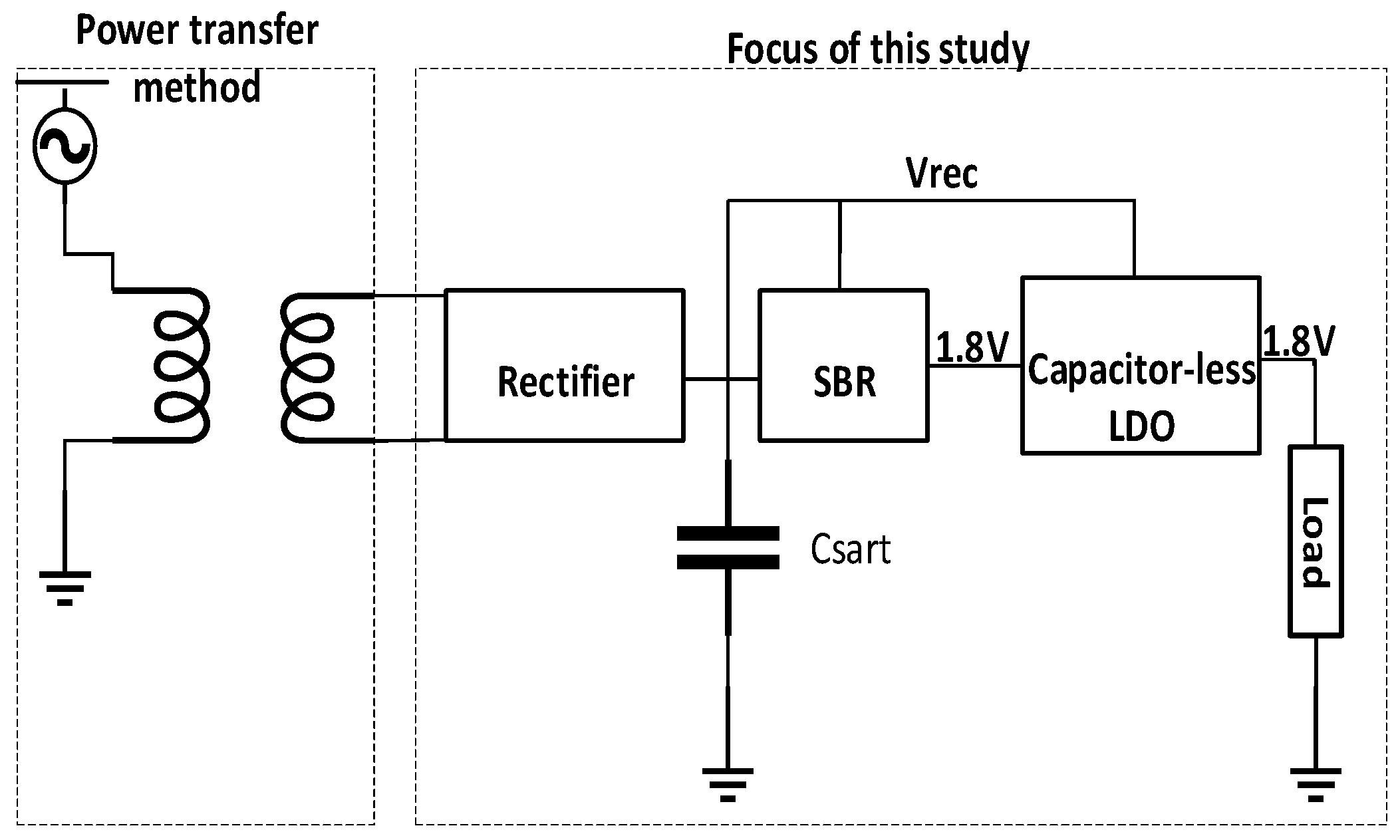
The overall functional diagram of the proposed self-powered power management system is shown in Figure 1. The effectiveness of a wireless power transmission system is a function of the transmitting unit, the receiving unit, and the interface circuitries. As shown in Figure 1, in this study, we focused exclusively on the circuit part of the wireless power receiving unit, and therefore, an ideal low-input current AC signal generated by a function generator, which can potentially be obtained by the acoustic, RF, or inductive coupling-based techniques, is used as an input voltage of the power management system. The proposed power management system includes three functional units: full-wave rectifier, self-biased CMOS reference voltage (SBR), and capacitor-less LDO. Each functional unit will be described in more detail below.

Figure 1.
Overall view of the proposed self-supplied power management system.
- A.
- Full-wave rectifier
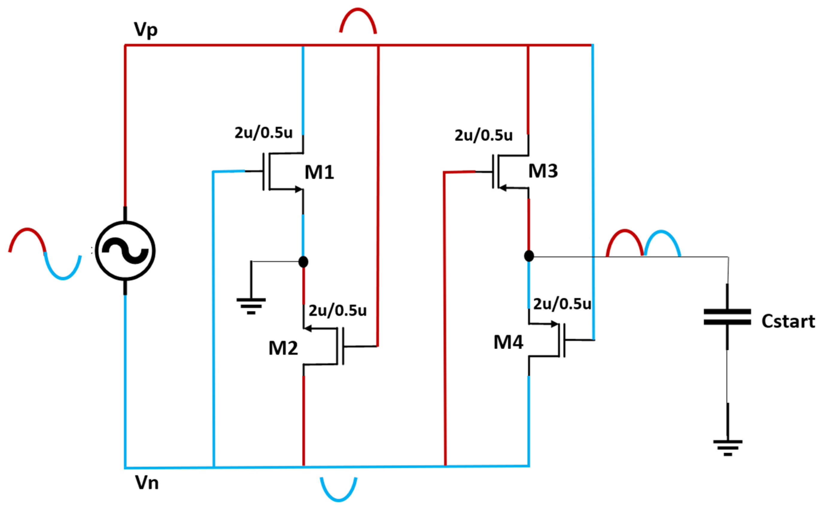
In the first stage, to convert the AC voltage received at the receiving unit into a DC signal, a full-wave rectifier is implemented with two pairs of N-channel and P-channel MOSFETs in a fully cross-coupled structure. The rectifier has a single stage, and as the input AC signal voltage is approximately 6.78 MHz, a smoothing capacitor can minimize ripples in the rectified voltage. The topology of the rectifier is shown in Figure 2, and was introduced by [25]. During the positive phase of the received AC signal, the transistors of M2 and M3 turn on and M1 and M4 turn off. This occurs because of the respective negative and positive voltage levels applied to their gates. Consequently, Vn is connected to the ground, and a current path is established through M3 to supply Vp to Cstart. This path is highlighted in red in Figure 2. Similarly, during the negative phase of the AC input signal, illustrated in blue in Figure 2, M1 and M4 turn on and M2 and M3 turn off. As a result, the reversed polarity of Vn is routed to Cstart through M4. This rectified voltage, Vrec, is accumulated in a 1 nF capacitor outside the chip, called Cstart. The power accumulated in the capacitor thus supplies power to the entire power management system, including the SBR and capacitor-less LDO. It is worth noting that all implemented transistors are thick oxide transistors with an overdrive voltage of 3.3 V to ensure system safety for a high input voltage [26].
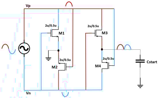
Figure 2.
Schematic of the deployed full-wave rectifier.
- B.
- Self-biased Reference Voltage (SBR)
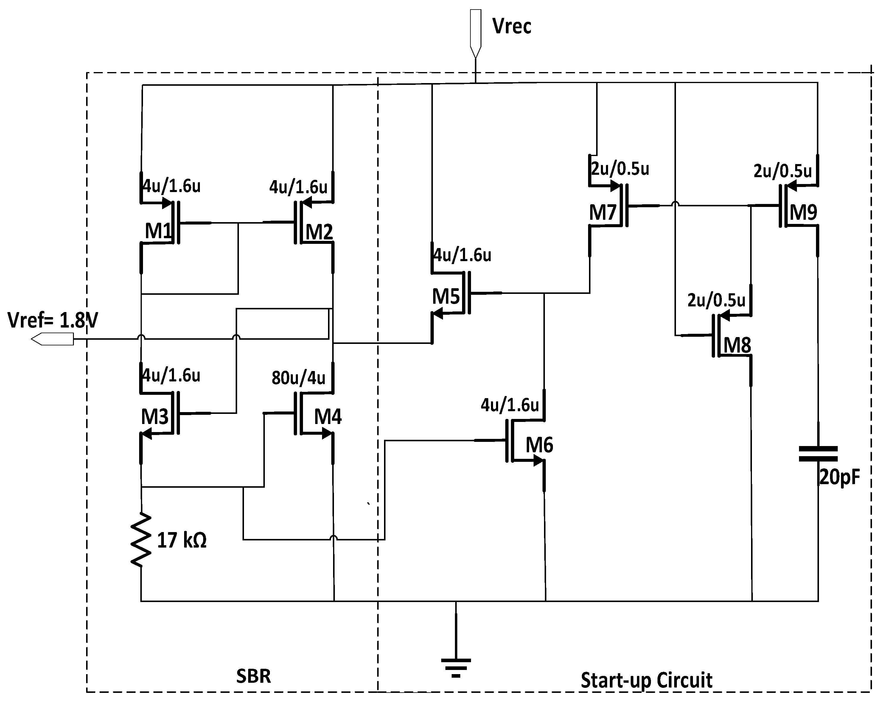
The circuit diagram of the implemented SBR and its transistor sizes are shown in Figure 3. This design is based on the earlier works presented in [27,28]. As can be seen in this figure, the implemented SBR is a Vgs referenced circuit. This means that the reference voltage is a function of the Vgs of transistors M3 and M4, and can be expressed as follows:
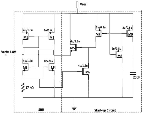
Figure 3.
Schematic of the deployed self-biased CMOS reference voltage (SBR) and its start-up circuit.
In this regard, it can be deduced that the size of the M3 and M4 channels plays a significant role in the overall performance of the SBR. Since the focus of this study is to deliver a fixed voltage of ~1.8 V to the load, the SBR transistors are designed to stabilize the rectified voltage Vrec to 1.8 V as the reference voltage, Vref.
- C.
- Capacitor-less LDO
A schematic of the proposed topology to create a capacitor-less LDO is shown in Figure 4a. According to this figure, the capacitor-less LDO comprises two transistors, where the first transistor M2_load is connected to the diode-connected M3_load with a common gate at the output node. The reason for using such a topology is that two MOSFETs connected at the output help minimize the fluctuations of the regulated voltage and, more importantly, the capacitances of these two transistors can appear as the dominant pole for the LDO feedback loop. Therefore, the stability of the LDO error amplifier (EA) feedback loop is improved even though the LDO has no large (~1 μF) load capacitance.
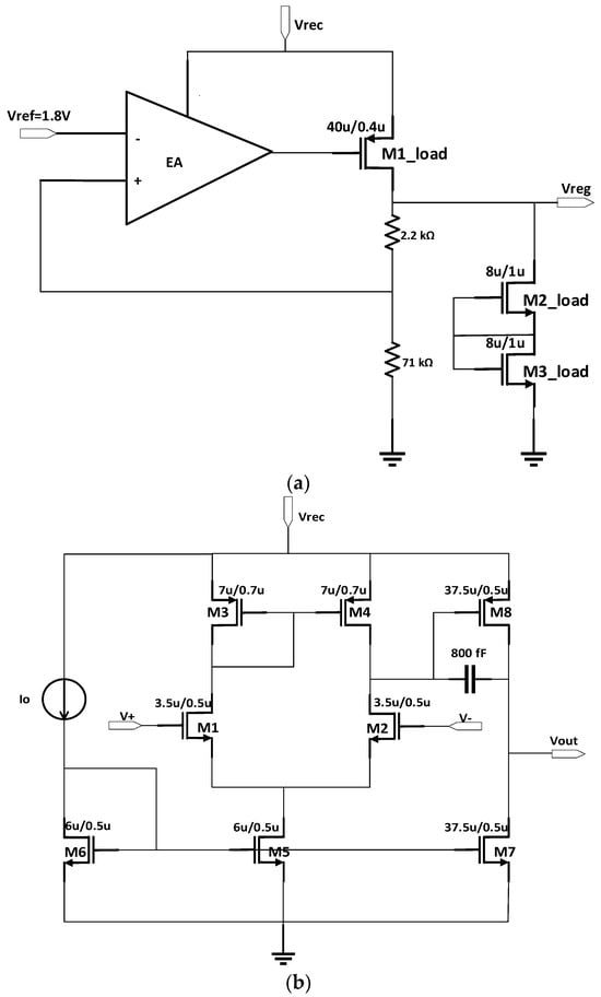
Figure 4.
Schematics of (a) the proposed capacitor-less LDO, and (b) its error amplifier.
The error amplifier is indeed a mandatory part of the LDOs. The schematic and transistor sizes of the EA we implemented are shown in Figure 4b. As can be seen, the EA is a two-stage operational amplifier. The size of the transistors was chosen to achieve a gain of more than 50 dB. In the simulation study, it is found that the maximum quiescent current of the capacitor-less LDO is 25.5 μA, while 0.5 and 2.2 pA of this amount were drawn by M2_load and M3_load, respectively. It can be concluded that the implemented load transistors of the capacitor-less LDO have a minimal contribution to the quiescent current.
3. Simulation Results
- A.
- Self-supplied power management system
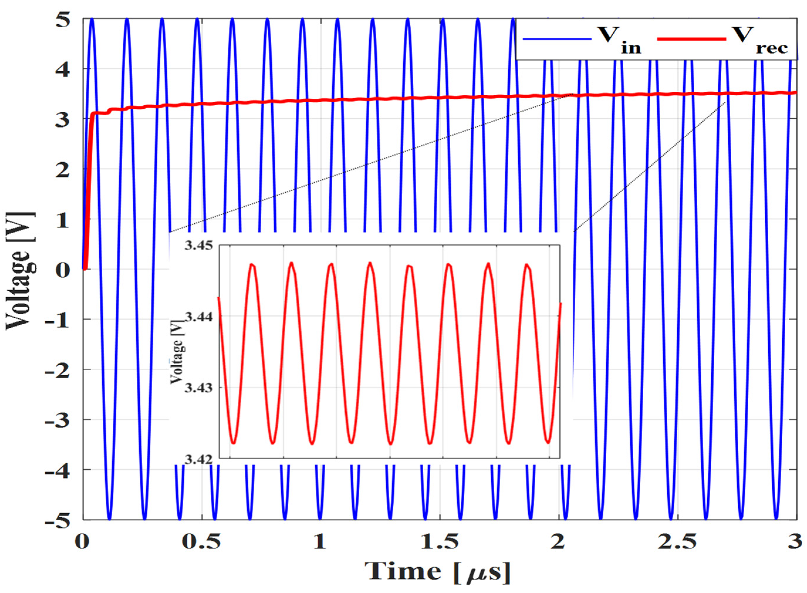
The functionality of the proposed power management system described in Section 2 was investigated by using Cadence Virtuoso software (version: IC6.1.8). In the first step, the capability of the implemented rectifier to convert AC signal to DC was surveyed. Figure 5 demonstrates the rectified voltage by our proposed full-wave rectifier when the peak amplitude of the AC input signal is 5 V at 6.78 MHz. It can be seen that after about 2 μs the level of the stored voltage in Cstart is fixed at 3.42 V. A comparison between the rms value of the input voltage and Vrec indicates that the voltage conversion efficiency of the rectifier is 96%. Moreover, its voltage ripple remains less than 20 mV.
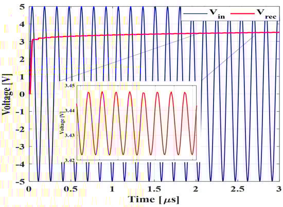
Figure 5.
Simulated rectified voltage Vrec by the proposed full-wave rectifier when the peak AC input voltage is 5 V at 6.78 MHz with demonstration of the ripple voltage.
- B.
- Self-biased Reference Voltage (SBR)
The ability of the implemented SBR to provide a reference voltage of about 1.8 V regardless of the amplitude of the input signal is shown in Figure 6. When the rectified voltage, Vrec, reaches 2.4 V, the SBR can effectively and accurately provide a fixed voltage of about 1.82 V, while further increasing Vrec has no effect on the SBR output voltage level. Consequently, this stable reference voltage can be fed into the next stage, i.e., the capacitor-less LDO.
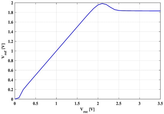
Figure 6.
Simulated reference voltage Vref when Vrec changes from 0–3.5 V.
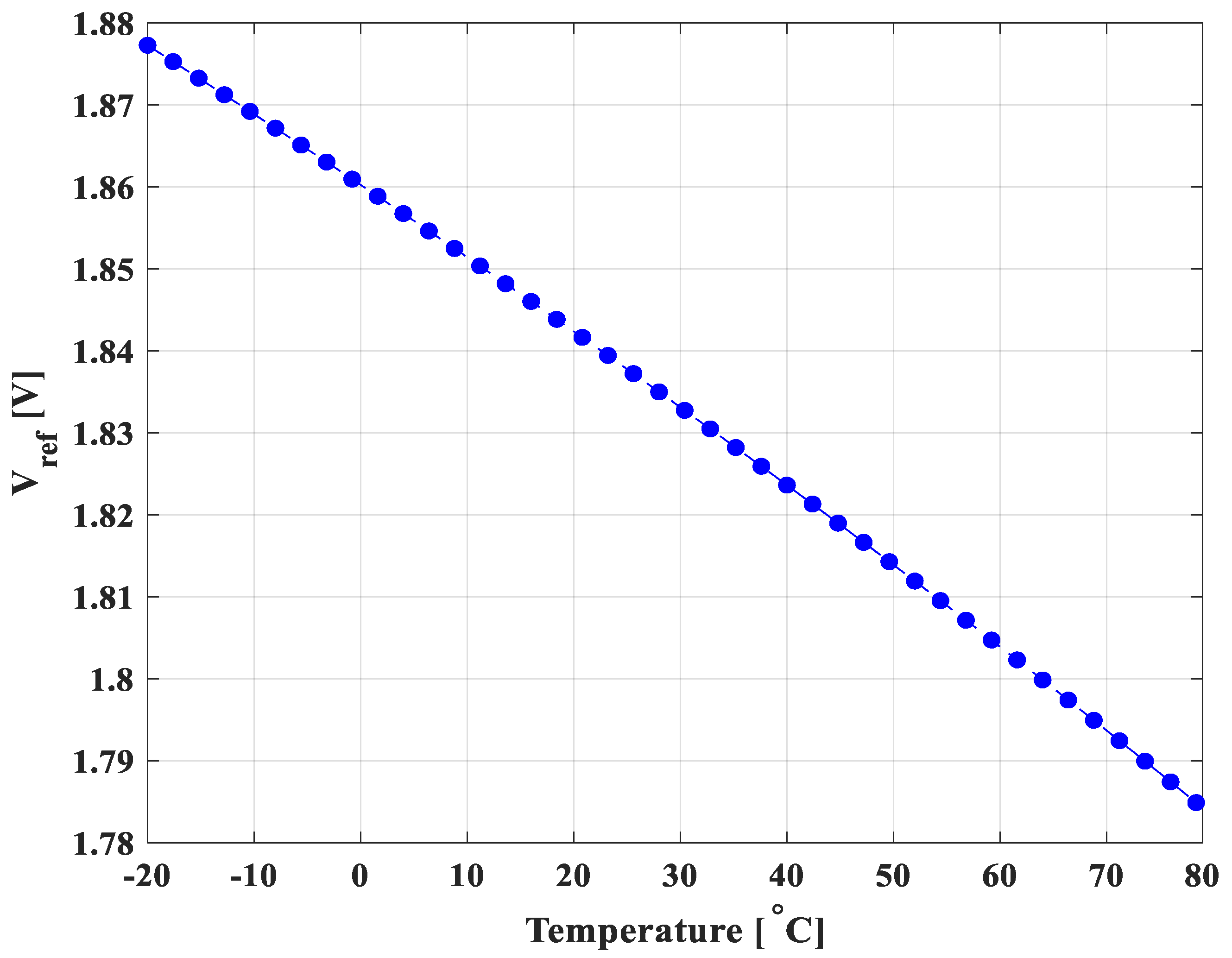
Figure 7 shows the simulated Vref over the extended temperature range of −20 to 80 was appropriate for biomedical devices when an input voltage of 3.3 V was applied to SBR. It is evident that Vref changes by 90 mV at this operating temperature, which corresponds to a deviation of 4.9% of its nominal voltage, i.e., 1.82 mV, at room temperature. It is worth noting that such a temperature coefficient is not necessarily low compared to ultra-low temperature coefficient reference voltage designs presented in the literature [29]. However, it should be taken into account that both the input voltage (3.3 V) and the reference voltage (1.8 V) of the implemented circuit in this work are relatively large compared to most of the highly stable reference voltage circuitries presented in the literature.
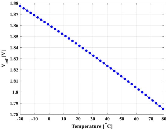
Figure 7.
Simulated reference voltage Vref when temperature varies from −20 to 80 °C at an input voltage of 3.3 V.
It is well known that Power Supply Ripple Rejection (PSRR) is a critical parameter in SBR circuitries. This metric measures the ripple of the output voltage compared to the input voltage over a relatively wide frequency range. The simulated PSRR shown in Figure 8 demonstrates that our implemented SBR exceeds −50 dB at frequencies below 3 MHz and drops to −48.8 dB at 7.9 MHz.
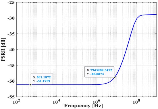
Figure 8.
Simulated PSRR of the implemented SBR. It achieves a PSRR of −48.8 dB at 7.9 MHz.
- C.
- Stability analysis of the capacitor-less LDO
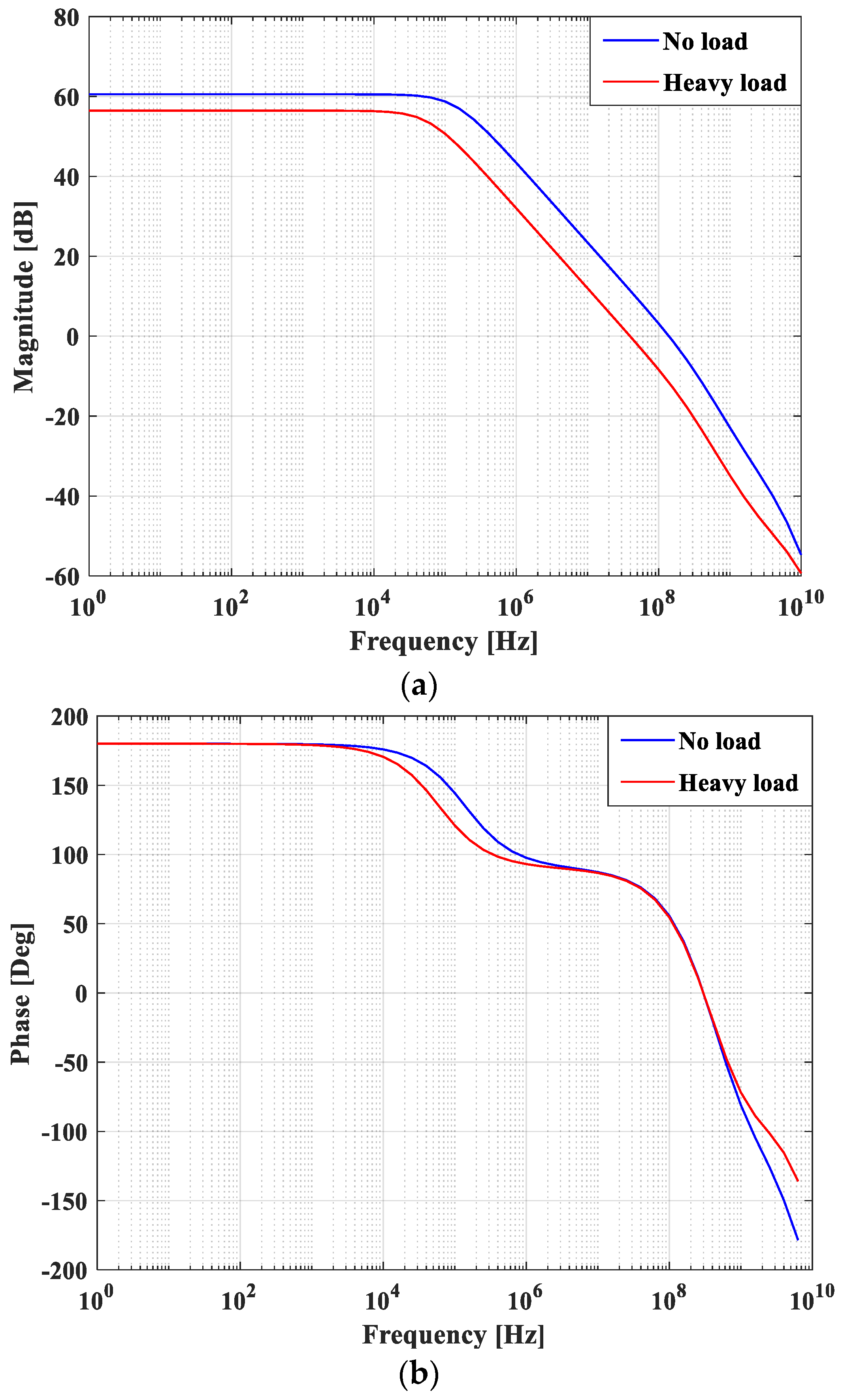
To confirm the stability of the proposed capacitor-less LDO under different load conditions, its open-loop gain was analyzed. The open-loop gain is shown in Figure 9. In this regard, the simulation was performed under two independent conditions, namely, no-current load and heavy load (more than 75 mA). In Figure 9a, the DC gain at heavy load is reduced from 60.5 to 56.43 dB under the no-load and heavy-load conditions, respectively. Similarly, the unit gain frequency is reduced by 99.5 MHz from 139 MHz to 39.5 MHz under the no-load and heavy-load conditions, respectively. The phase analysis shown in Figure 9b reveals that the phase margin at zero load and heavy load is 43 and 75 degrees, respectively. The high open-loop gain and large phase margin confirm the stability of the capacitor-less LDO at all times.
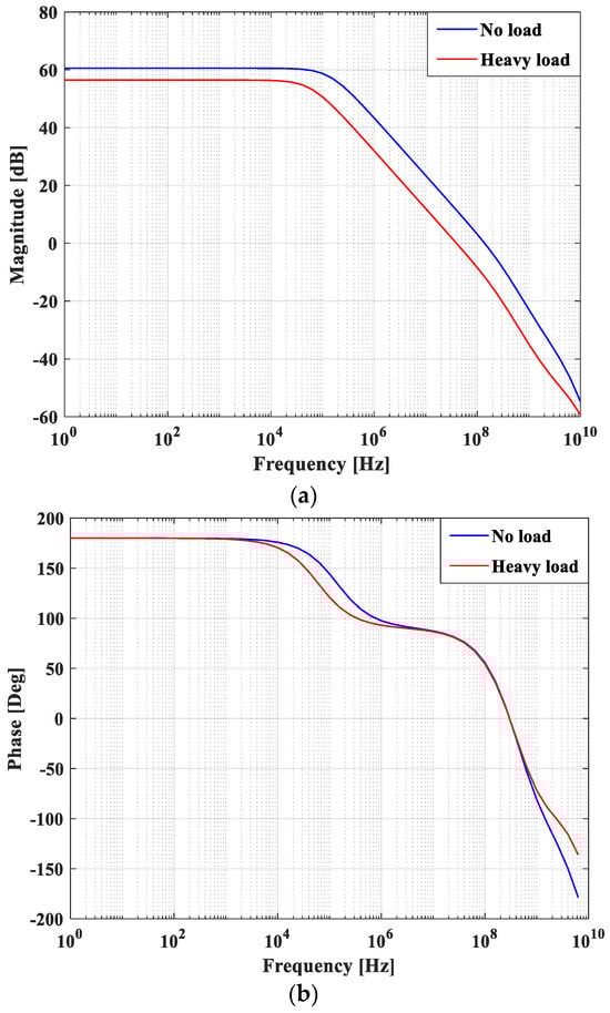
Figure 9.
Simulated (a) magnitude and (b) phase open loop gain of the proposed capacitor-less LDO at different load conditions.
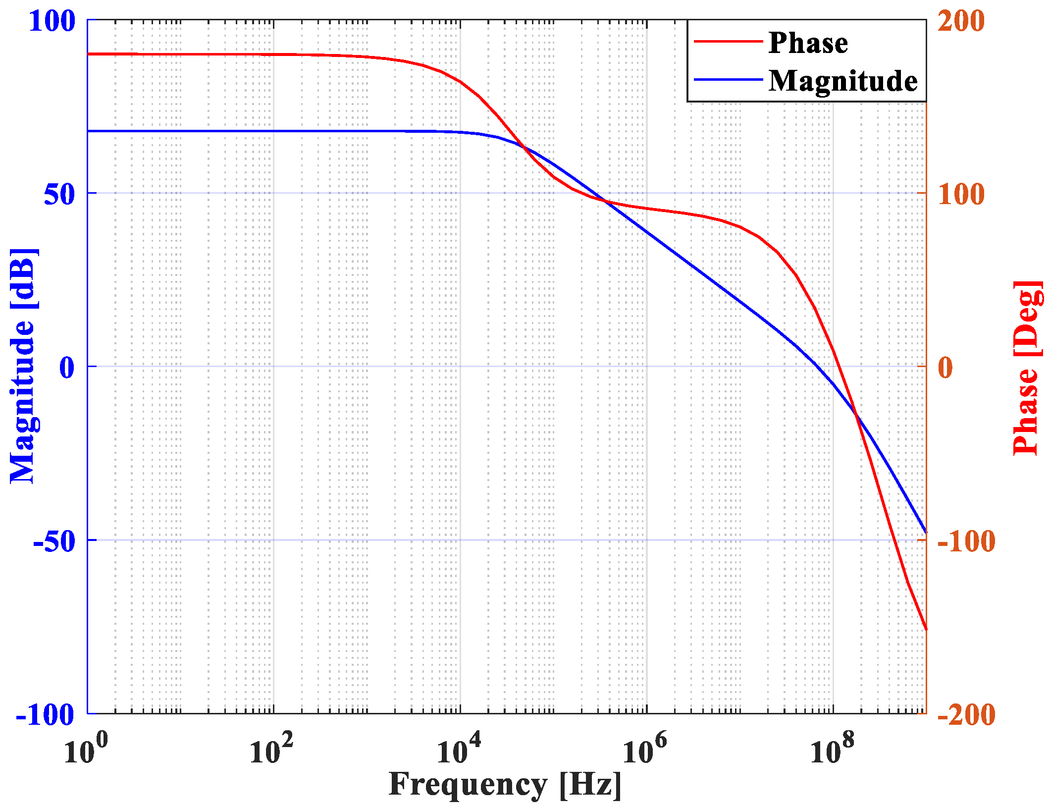
It should not be ignored that real consumer electronics typically contain an input capacitor that serves as a load capacitor for the LDOs. To ensure that the capacitive loads do not affect the stability of our proposed capacitor-less LDO, the open-loop gain of the capacitor-less LDO was investigated at heavy current and in the presence of a load capacitor of 100 pF. As shown in Figure 10, the load capacitance indeed results in a DC gain and phase margin of 55 dB and 30.4 deg, respectively. Since both gain and phase margin are sufficiently high even when a load capacitor is connected to the capacitor-less LDO, its stability under capacitive loads is assured [24].
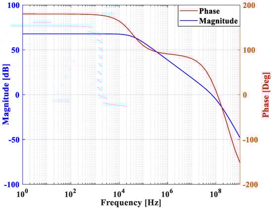
Figure 10.
Simulated open loop gain of the proposed capacitor-less LDO at heavy load condition and load capacitor of 100 pF.
- D.
- Process variations analysis
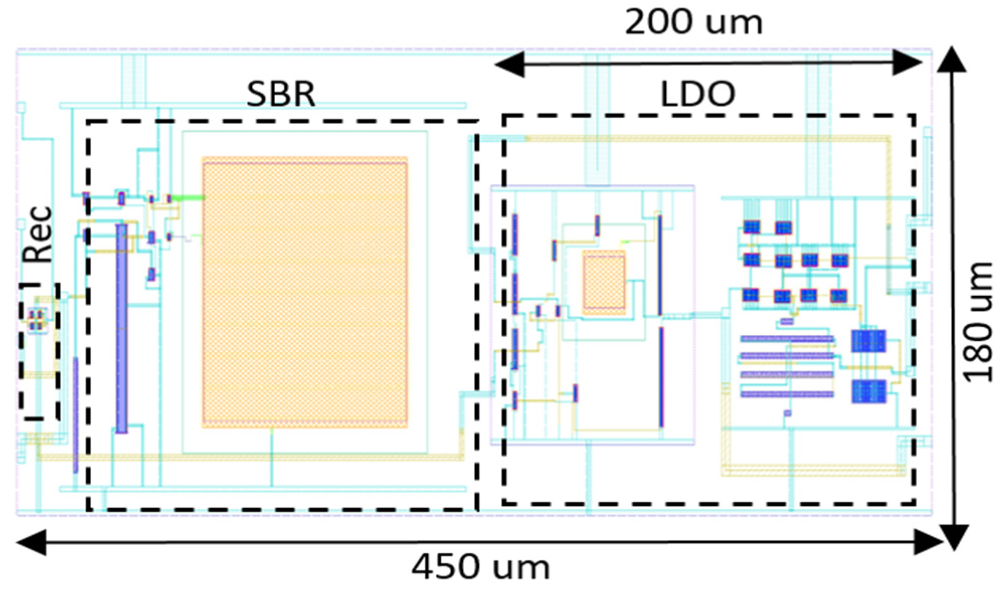
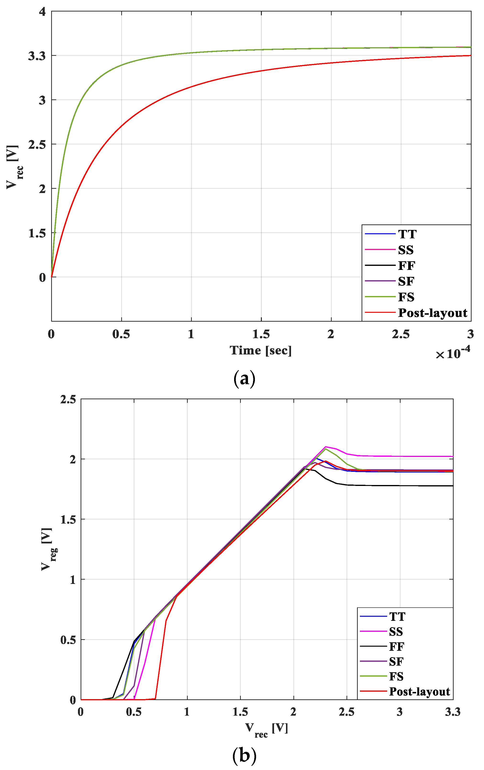
Figure 11 shows the layout diagram of the proposed power management system. The overall active area of the system is 450 μm × 180 μm and can be manufactured by TSMC 65 nm technology. In order to show that the power management system is relatively insensitive to process variations, Figure 12 displays the schematic results at different corners, namely, typical-typical (TT), slow-slow (SS), fast-fast (FF), fast-slow (FS), and slow-fast (SF), for the rectified voltage with an input AC signal of 5 V at 6.78 MHz and the regulated voltage as a function of the rectified voltage, respectively. In addition, this figure includes the post-layout simulations. It can be concluded that the rectifier design is very robust to process variations, as no significant changes in the amplitude of the rectified voltage are observed at any analyzed corner. However, the post-layout result shows a slightly lower rectified voltage compared to the schematic. This is mainly due to the parasitic capacitances caused by the traces. The rectified voltages at the different corners shown in Figure 12b indicate that the maximum deviation of the regulated voltage belongs to the FF and SS corners. In this regard, the output signal of the power management can only change by ±13% (~250 mV). Consequently, the proposed power management system is relatively insusceptible to the process variations.
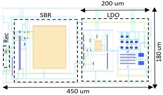
Figure 11.
Layout of the self-supplied power management system.
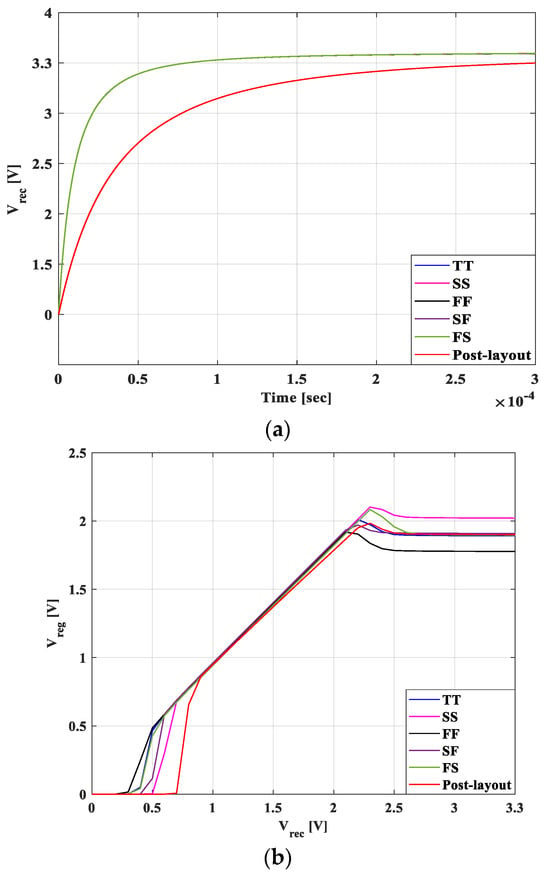
Figure 12.
Schematic at different corners and post-layout simulations for (a) the rectified voltage when the input peak AC signal is 5 V at a frequency of 6.78 MHz and (b) the regulated voltage Vreg for different rectified voltages.
4. Experimental Results
- A.
- Apparatus
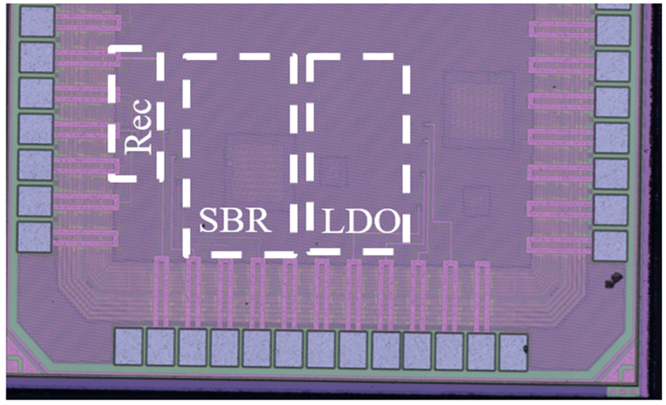
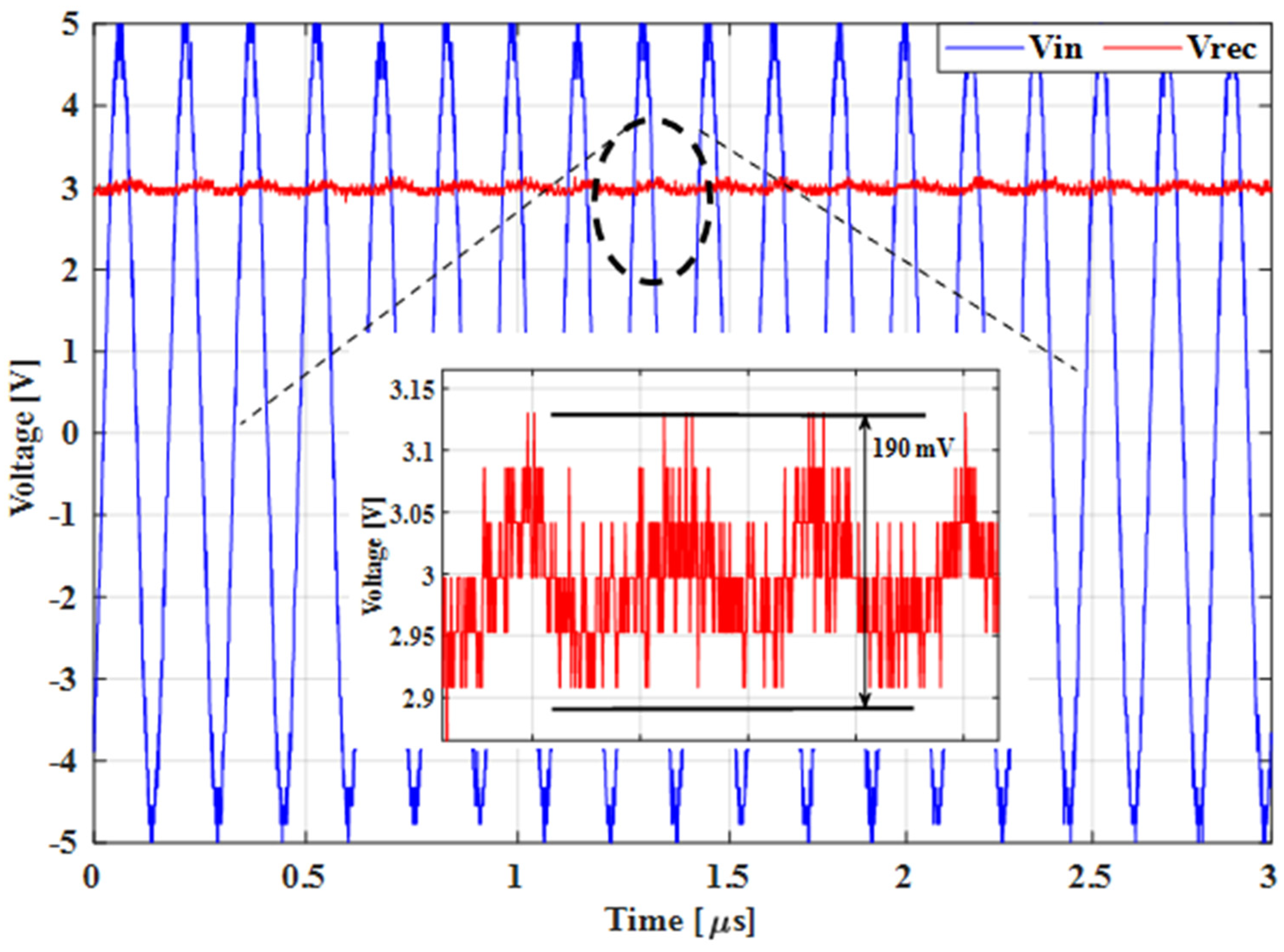
To validate the simulation results presented in the previous section, the power management system was fabricated using a standard 65-nm CMOS microfabrication technology from TSMC. Figure 13 shows the micrograph of the fabricated chip. The first step was to investigate the ability of the power management system to rectify different AC input signals. To do this, an AC signal with a varying peak amplitude of 1.5–5 V at a constant frequency of 6.78 MHz was applied to the chip using a function generator manufactured by Rohde & Schwarz (model A000). The rectified voltage, Vrec, across the capacitor Cstart was then measured using an oscilloscope from Tektronix (model DPO3032). Figure 14 illustrates the measured Vrec when an AC input signal of 5 V was applied. From this figure, it can be seen that the rectified DC voltage at Cstart is 3.12 V. This signifies that the voltage conversion efficiency of the rectifier is 89%, while the voltage ripple is less than 6% of the rectified signal amplitude. A holistic comparison between the simulated and measured Vrec values shows that our simulation study can estimate the behavior of the rectifier with an error of 7% compared to the values obtained from the prototype measurement. It should be noted that in this manuscript, the amplitude of the AC signal, Vin, is the peak amplitude.
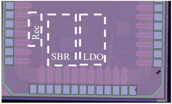
Figure 13.
Micrograph of the fabricated chip in 65 nm process technology.
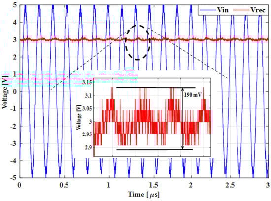
Figure 14.
Measured rectified voltage Vrec by the proposed full-wave rectifier when the peak AC input voltage Vin is 5 V at 6.78 MHz with demonstration of the ripple voltage.
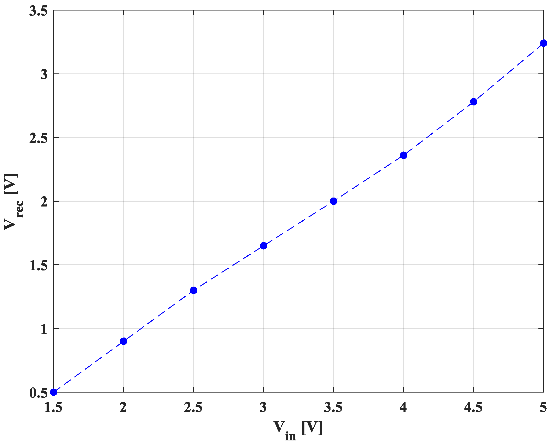
Figure 15 shows the measured DC voltage rectified by the implemented full-wave rectifier when the input AC signal Vin varies from 1.5 V to 5 V. This figure shows that the rectifier has a fairly linear efficiency and can easily supply a DC voltage of up to ~3.3 V to the load capacitor. Therefore, for simplicity, Vrec, the rectified AC signal from Vin, will be considered the input signal to the SBR and the capacitor-less LDO units of the power management system in the remainder of this article.
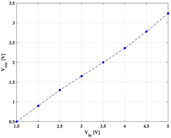
Figure 15.
Measured rectified voltage Vrec as a function of AC input signal Vin at a frequency of 6.78 MHz.
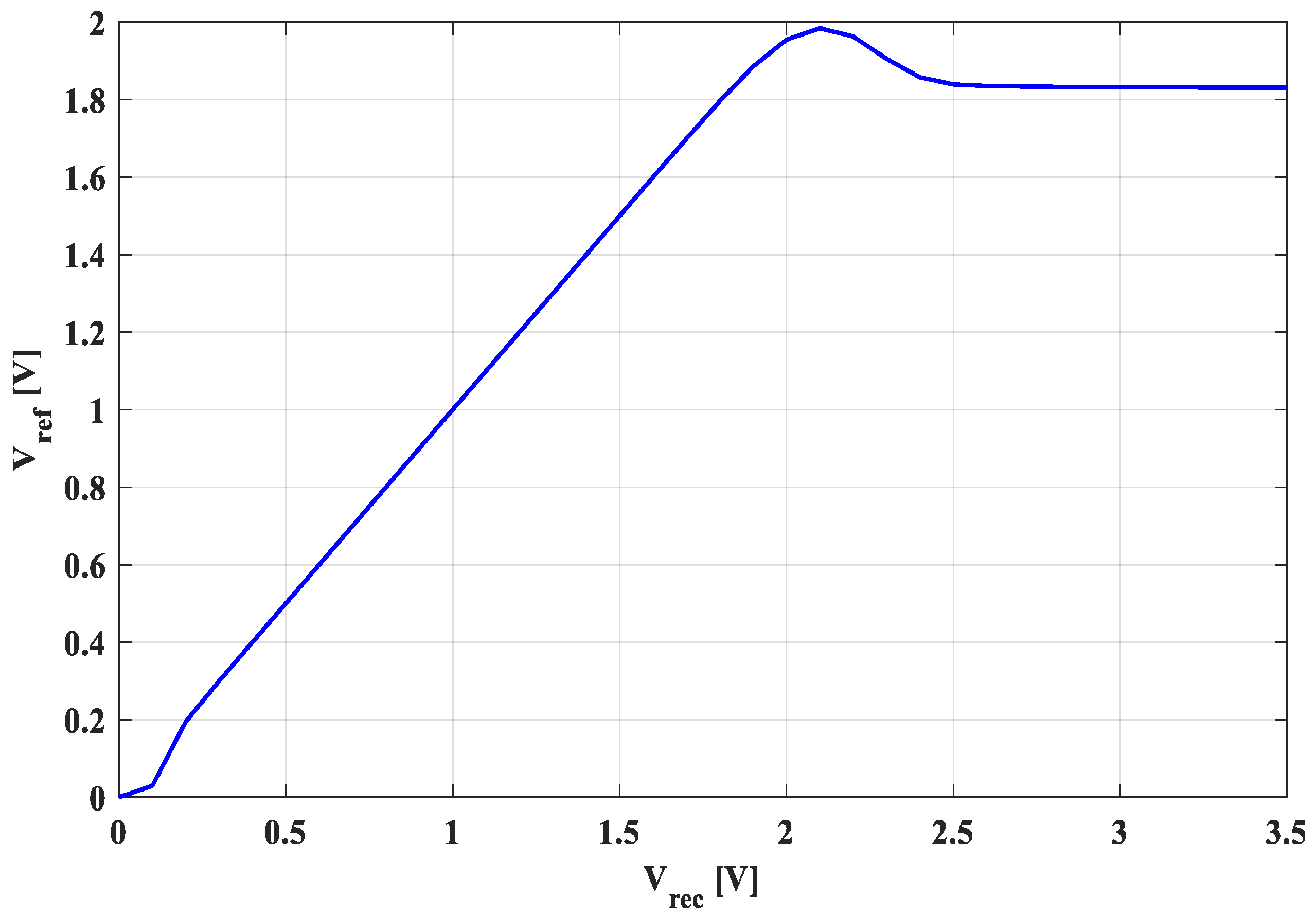
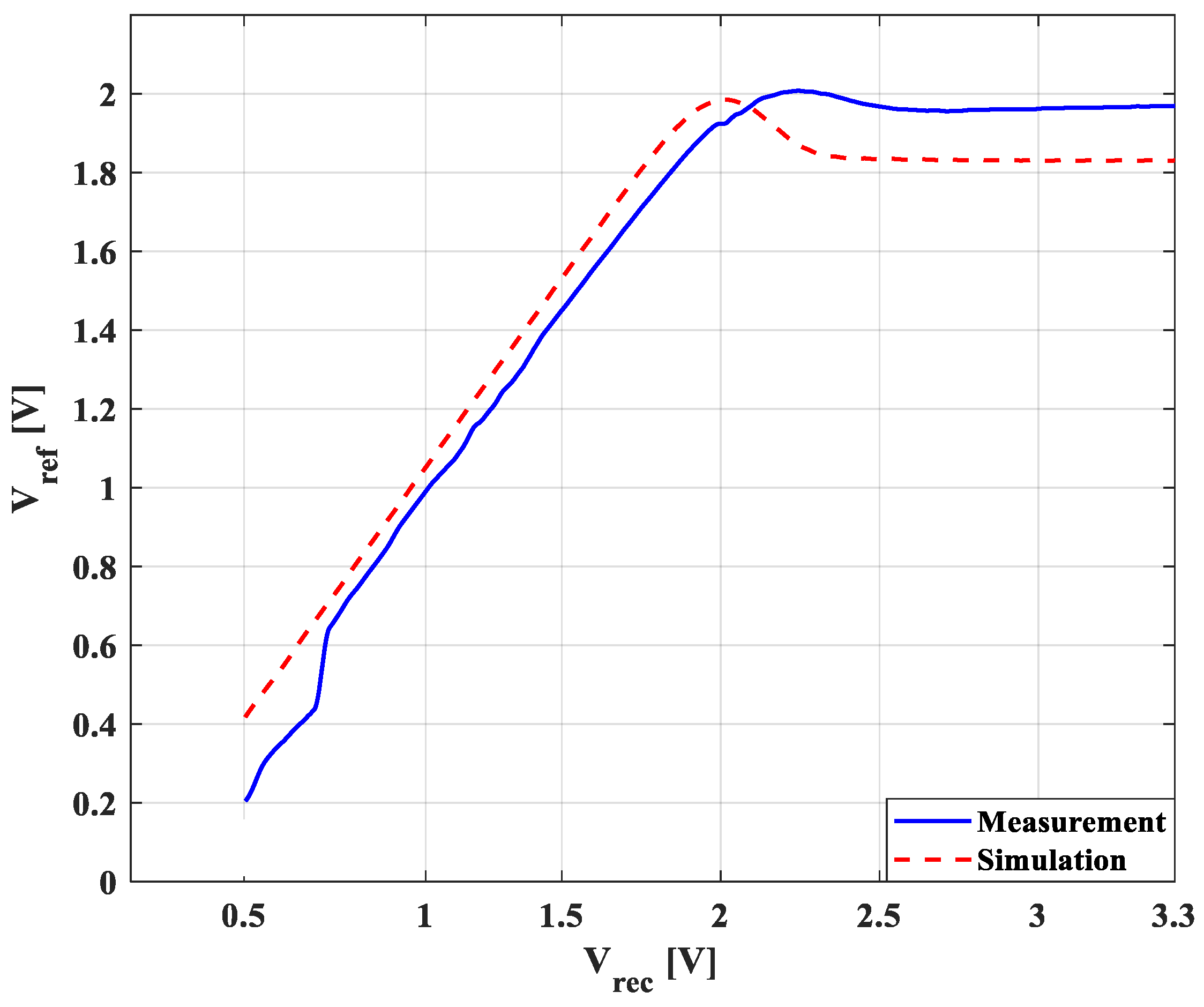
The measured Vref as a function of Vrec values is shown in Figure 16. It can be seen that an increase in Vrec increases the level of Vref. However, when Vrec reaches a voltage of 2.5 V, the reference voltage Vref remains almost at the constant voltage level of 1.91 V. It can also be seen that further increasing Vrec to 3.3 V does not considerably change the amplitude of Vref, less than 2 mV. It is worth mentioning that such a behavior was predicted by our simulation study. Hence, it can be concluded that the simulation model that was used for the implemented SBR has an acceptable level of accuracy.
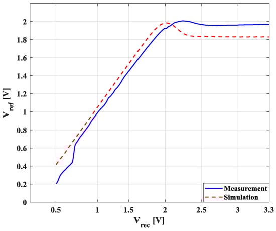
Figure 16.
Measured and simulated reference voltage Vref when the rectified voltage Vrec varies from 0.5 to 3.3 V.
The overall ability of the power management system to regulate and deliver a fixed voltage to an open-circuit load for various rectified voltages is shown in Figure 17a. It can be seen that the power management system is capable of delivering a fixed DC voltage of 1.75 V when the rectified voltage has an amplitude greater than 2.5 V (indicating an AC voltage of 4.2V). Increasing the rectified voltage to 3.3 V changes the regulated voltage by only 2 mV to 1.77. In this case, it was observed that the quiescent current increases from 25 μA to 55 μA. It can be deduced that the input AC signal requires peak amplitudes ranging from a minimum of 4.2 V to a maximum of 5 V.
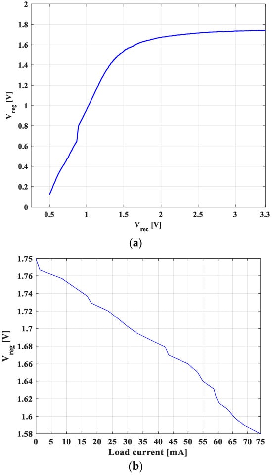
Figure 17.
Measured (a) regulated voltage Vreg for different rectified voltages Vrec at the load current of zero and (b) variable load currents when the regulated voltage is 3.3 V.
To confirm that the power management system can deliver a wide range of currents to the load and such a competence is indeed not dependent on the load, the behavior of the power management system for the variable load currents is shown in Figure 17b. Clearly, the power management system can deliver a current in the range of 0–75 mA, and in this wide dynamic operating range, the amplitude of the regulated voltage changes by 170 mV, from 1.75 V to 1.58 V. Consequently, the measured load regulation and line regulation of the power management system are 2.2 mV/mA and 0.8 mV/V, respectively.
- B.
- Line regulation and load regulation measurements
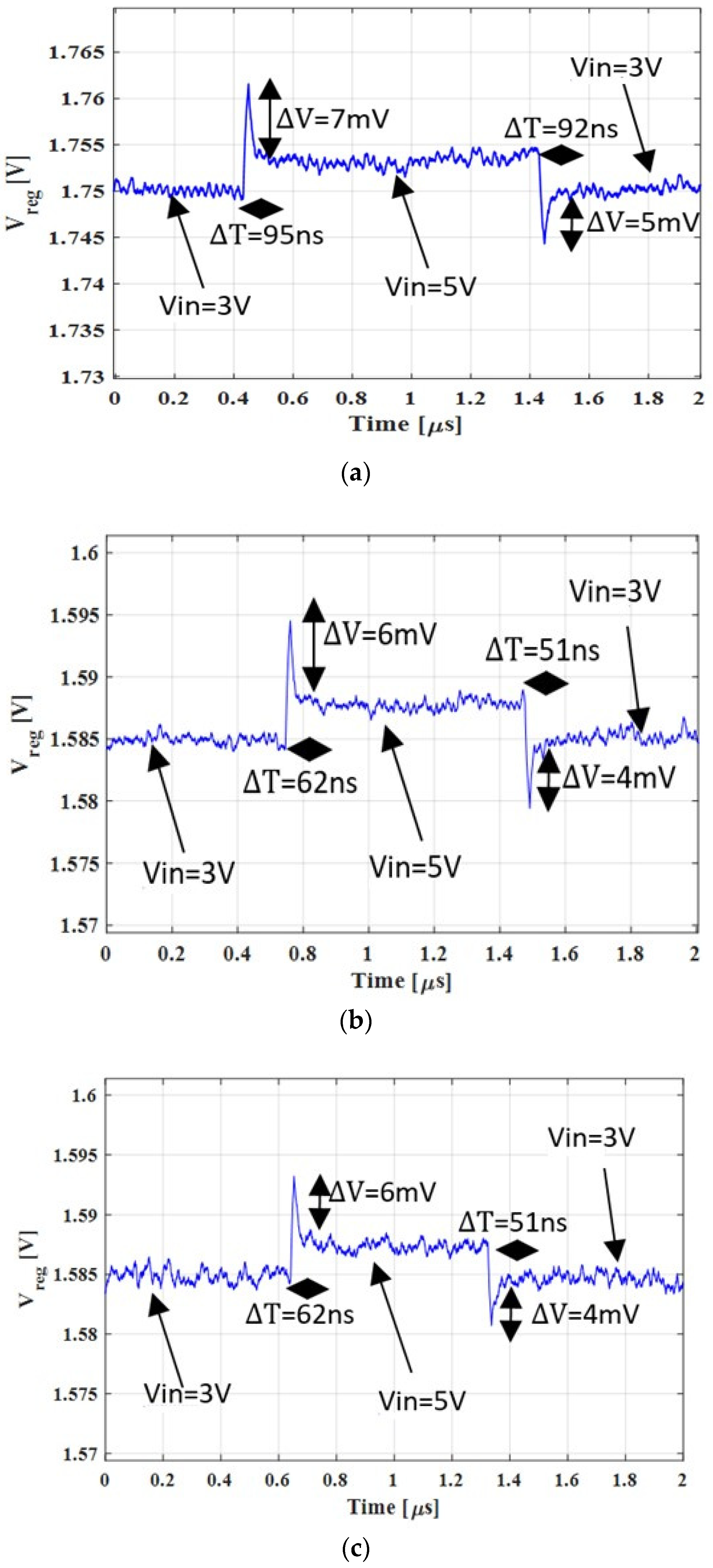
The line regulation time response measured under different load conditions, namely, zero, 75 mA, and 75 mA with a load capacitor of 100 pF, for the capacitor-less LDO when the input voltage changes from 2.5 V to 3.3 V is shown in Figure 18. It can be seen that when the voltage level is changed from low to high, i.e., from 2.5 V to 3.3 V, an overshoot of less than 15 mV is observed in all load conditions. It is worth mentioning that the maximum overshoot belongs to the load capacitor, where the Vreg is stabilized in less than 160 ns. Changing the input level from a high to a low level causes a maximum undershoot of about 11 mV, which is reduced to 4 mV at a load current of 75 mA with a load capacitance of 100 pF. It can be concluded that the existence of a load capacitor almost has no impact on the load line time response of the capacitor-less-LDO.
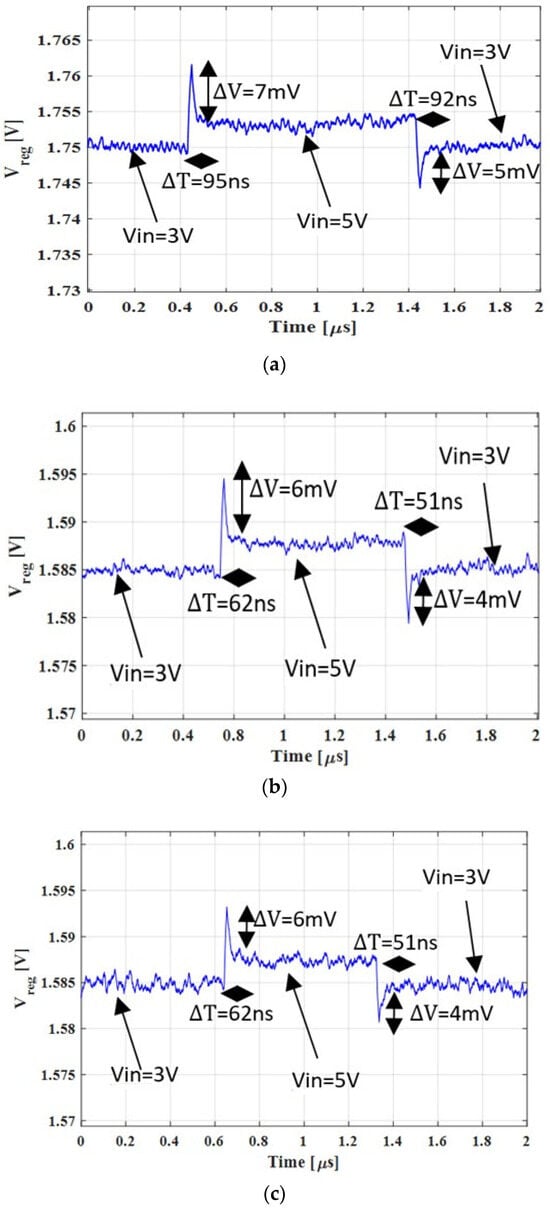
Figure 18.
Measured time response of the line regulation under different load conditions: (a) no load, (b) 75 mA load, and (c) 75 mA load with 100 pF load capacitor.
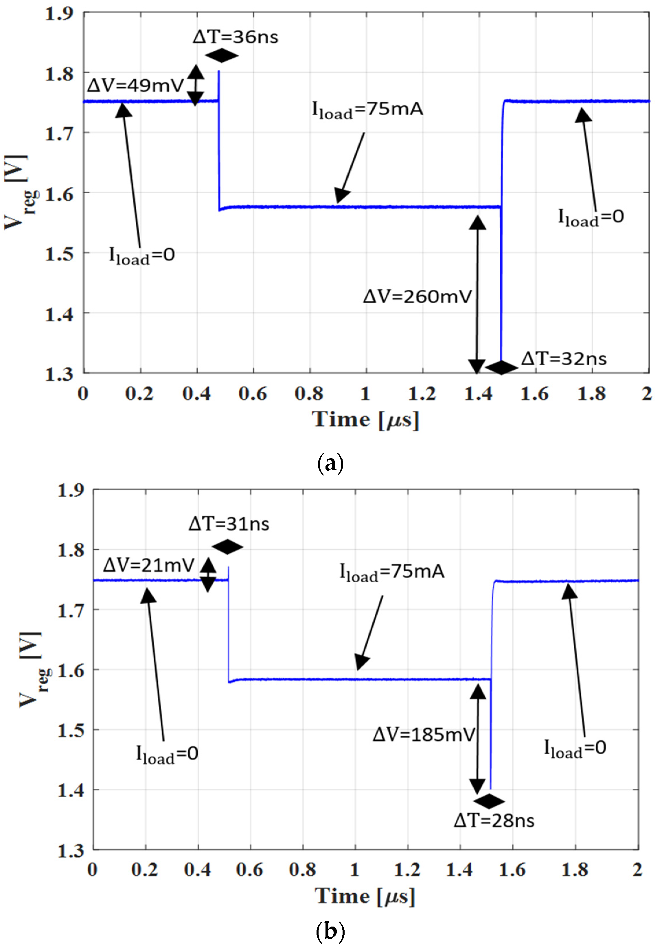
The measured time response of the load regulation with and without a load capacitor when the load current changed from 0 to 75 mA is shown in Figure 19. It can be clearly seen that the change of the load current state from 0 to 75 mA when there is no load capacitor leads to an overshoot of 49 mV. On the other hand, in this condition, changing the current state from 75 mA to 0 results in an undershoot of 260 mV, where the load current has stabilized after almost 36 ns, as this figure shows. It is worth mentioning that a load capacitance of 100 pF leads to a reduction in overshoot and undershoot by 42% and 71%, respectively. It can be concluded that a load capacitor can minimize the changes to Vreg when the load current level suddenly varies. As such, the load capacitor does not degrade the overall performance of the capacitor-less LDO.
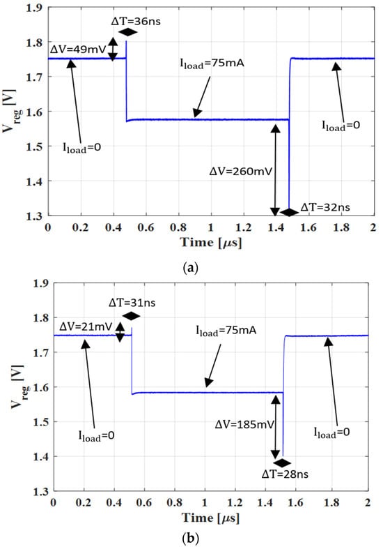
Figure 19.
Measured time response of the load regulation (a) without load capacitor and (b) with load capacitor of 100 pF.
- C.
- Temperature sensitivity measurement
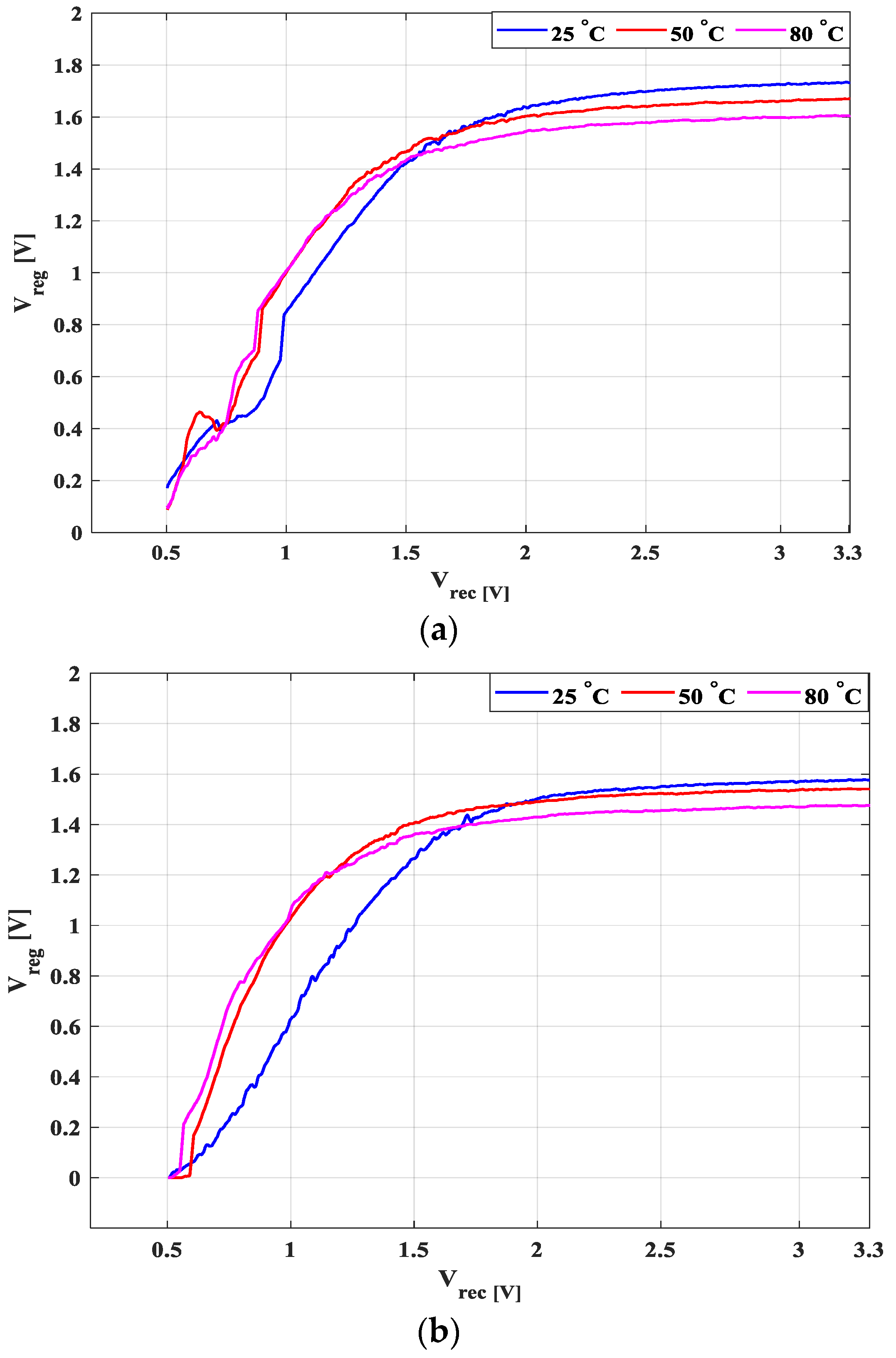
To this end, it is comprehensively demonstrated that the proposed power management system can rectify and effectively regulate the input AC signal to a constant DC voltage. To show the relatively stable performance of the power management system at different environment temperatures, the regulated voltage Vreg was measured at various temperatures, namely, room temperature, 50 °C, and 80 °C, as a function of Vrec at two standalone load currents of zero and 75 mA. According to Figure 20a, we can see that at a load current of zero increasing the temperature from room temperature, i.e., 25 °C to 50 °C results in a drop in Vreg to 1.68 V, and a further increase of the temperature to 80 °C reduces Vreg to 1.62 V. This means that a 55 °C increase in ambient temperature degrades the power management system’s performance in rectifying and regulating the AC input signal by 9% compared to data obtained at the temperature for which the system was originally designed, i.e., room temperature. The power management system exhibited a similar behavior at a load current of 75 mA. As shown in Figure 20b, the regulated voltage is 1.58 V at 25 °C and drops to 1.49 V at a temperature of 80 °C. This 90 mV reduction in the regulated voltage means that the overall power management system performance is reduced by 6% when its peripheral temperature changes from 25 °C to 80 °C.
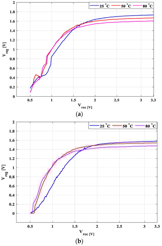
Figure 20.
Measured regulated voltage Vreg at different temperatures for load currents of (a) zero and (b) 75 mA.
- D.
- Case study
To further demonstrate that the power management system proposed in this study is a practical solution for powering wearables and IMDs, a commercially available low-power humidity and temperature sensor manufactured by Sensirion was integrated with the power management system. In this experiment, the sensor was powered through the output of the power management system, Vreg, while the power management system was supplied with an AC signal of 5 V. We performed the measurements at two different temperatures, i.e., 25 °C and 50 °C, by placing the power management system and the temperature sensor on the surface of a hot plate. In this experiment, the maximum temperature of 50 °C was chosen, since the commercially available sensor can only operate in a temperature range of 0 °C to 50 °C. Figure 21 shows our measurement setup and the level of Vreg monitored by the oscilloscope over a period of 2 min. It can be clearly seen that the voltage supplied to the load is considerably stable during measurement at both temperatures, as there are no sudden fluctuations in the measured signals. We can also see that the power management system is able to provide sufficient power to the load, as the performance of the sensor was not affected, which means that it was capable of measuring the humidity and temperature and displaying them on the LCD.
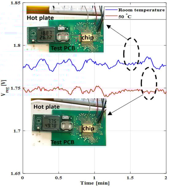
Figure 21.
Measured regulated voltage Vreg when the commercial sensor is used as the load. The measurements were performed at two different temperatures, and the sensor’s LCD clearly displays the actual humidity and temperature, respectively.
- E.
- Comparison with the literature
To further show the competence of the proposed capacitor-less LDO, its performance parameters are summarized in Table 1 and compared with the LDOs recently published in the literature. At a glance, it can be seen that our capacitor-less LDO is the only circuit that can regulate a wide range of input signals i.e., 2.5–3.3 V. At the same time, this unique feature does not deteriorate other important characteristics such as dropout voltage, line regulation, and PSSR. On the other hand, the regulation line of our capacitor-less LDO is not as low as that of its counterparts. Further reduction of the load regulation in the future will improve the superiority of the capacitor-less LDO. It is worth noting that the LDO proposed in [30] is capable of delivering 2.6 times higher current to the load than our power management system. However, it should not be ignored that this circuit has a high quiescent current (i.e., 2.9 times higher than the system proposed in this work) and the input voltage is limited to a relatively small range, 0.7 V, and requires a large load capacitor.

Table 1.
Performance comparison of the proposed capacitor-less LDO with state-of-the-art.
Up to now, the performance of the power management system has been investigated through comprehensive simulation studies and prototype measurements in different scenarios. To highlight its suitability as an efficient system for providing stable and reliable voltage/power to consumer electronics, the overall performance of the implemented self-powered energy management system is compared with the systems presented in the literature. Table 2 summarizes this comparative study. It is obvious that the self-powered power management system implemented in this study occupies a very small silicon area compared to its counterparts. Moreover, the system presented in this work can deliver a relatively high current to the load. It is worth mentioning that the power management system presented in [36] is an efficient solution for delivering a large amount of current to the load. It cannot be ignored that the rectification mechanism used in this system is based on a series-resonant rectifier. Furthermore, the regulation is undertaken via a DC-DC converter, which is inherently very power hungry and less attractive for portable and implantable biomedical devices with low power consumption [37].
Table 2.
Performance comparison of the proposed self-supplied power management system with state-of-the-art integrated power management systems.
5. Conclusions and Future Work
In this work, a self-supplied power management system for wirelessly powered/recharged biomedical devices is proposed. The proposed system consists of three functional units, namely, a fully cross-coupled MOSFET rectifier, an SBR, and a capacitor-less LDO. In order to minimize the complexity of the conventional capacitor-less LDOs, a novel architecture based on a pair of diode-connected transistors at the load is proposed. This eliminates the requirement of the load capacitor. The overall behavior of the power management system for rectifying and regulating an AC input signal into a DC signal was investigated numerically and experimentally. A prototype of the power management system was implemented in the 65 nm CMOS process from TSMC with an active chip area of 0.0810 mm2. Results indicate that the power management system can rectify an AC signal in the range of 4.25–5 V and regulate it to a fixed DC voltage of 1.75 V. It is shown that the power management system can deliver current in the range of 0–75 mA with a maximum voltage drop of 170 mV. Eventually, the suitability of the power management system for driving low-power consumer electronics devices was demonstrated and its versatility compared to state-of-the-art integrated power management systems was discussed.
Looking forward to our future work, we intend to extend the versatility of the proposed self-powered power system by improving its load regulation and thermal stability while maintaining its wide input voltage operation. One possible technique to minimize load regulation is to introduce multipoles in the LDO topology. Thermal stability can be achieved by using a reference circuit with a better thermal coefficient.
Author Contributions
Conceptualization, S.N. and S.B.; methodology, S.N.; writing—original draft preparation, S.N.; review and editing, S.B. All authors have read and agreed to the published version of the manuscript.
Funding
The research was supported by the Natural Sciences and Research Council of Canada (fund number 250089), MEDTEQ (fund number 250706), and industrial partners: iMD Research (fund number 250707) and Metropole Dentaire Terrebonne (fund number 250708).
Data Availability Statement
The data that support the findings of this study are available from the corresponding author upon reasonable request.
Conflicts of Interest
The authors declare no conflict of interest.
References
- Hooshmand, M.; Zordan, D.; Del Testa, D.; Grisan, E.; Rossi, M. Boosting the Battery Life of Wearables for Health Monitoring through the Compression of Biosignals. IEEE Internet Things J. 2017, 4, 1647–1662. [Google Scholar] [CrossRef]
- Li, Y.; Fu, J.; Zhong, C.; Wu, T.; Chen, Z.; Hu, W.; Amine, K.; Lu, J. Recent Advances in Flexible Zinc-Based Rechargeable Batteries. Adv. Energy Mater. 2019, 9, 1802605. [Google Scholar] [CrossRef]
- Karimi, M.J.; Schmid, A.; Dehollain, C. Wireless Power and Data Transmission for Implanted Devices via Inductive Links: A Systematic Review. IEEE Sens. J. 2021, 21, 7145–7161. [Google Scholar] [CrossRef]
- Jia, Y.; Mirbozorgi, S.A.; Zhang, P.; Inan, O.T.; Li, W.; Ghovanloo, M. A Dual-Band Wireless Power Transmission System for Evaluating Mm-Sized Implants. IEEE Trans. Biomed. Circuits Syst. 2019, 13, 595–607. [Google Scholar] [CrossRef] [PubMed]
- Lyu, H.; Babakhani, A. A 13.56-MHz −25-dBm-Sensitivity Inductive Power Receiver System-on-a-Chip With a Self-Adaptive Successive Approximation Resonance Compensation Front-End for Ultra-Low-Power Medical Implants. IEEE Trans. Biomed. Circuits Syst. 2020, 15, 80–90. [Google Scholar] [CrossRef]
- Manoufali, M.; Bialkowski, K.; Mohammed, B.J.; Mills, P.C.; Abbosh, A. Near-Field Inductive-Coupling Link to Power a Three-Dimensional Millimeter-Size Antenna for Brain Implantable Medical Devices. IEEE Trans. Biomed. Eng. 2017, 65, 4–14. [Google Scholar] [CrossRef]
- Luo, Y.-S.; Wang, J.-R.; Huang, W.-J.; Tsai, J.-Y.; Liao, Y.-F.; Tseng, W.-T.; Yen, C.-T.; Li, P.-C.; Liu, S.-I. Ultrasonic Power/data Telemetry and Neural Stimulator with OOK-PM Signaling. IEEE Trans. Circuits Syst. II Express Briefs 2013, 60, 827–831. [Google Scholar] [CrossRef]
- Kiani, M.; Ghovanloo, M. An RFID-Based Closed-Loop Wireless Power Transmission System for Biomedical Applications. IEEE Trans. Circuits Syst. II Express Briefs 2010, 57, 260–264. [Google Scholar] [CrossRef]
- Wei, X.; Liu, J. Power Sources and Electrical Recharging Strategies for Implantable Medical Devices. Front. Energy Power Eng. China 2008, 2, 1–13. [Google Scholar] [CrossRef]
- Basaeri, H.; Christensen, D.B.; Roundy, S. A Review of Acoustic Power Transfer for Bio-Medical Implants. Smart Mater. Struct. 2016, 25, 123001. [Google Scholar] [CrossRef]
- Shen, K.; Maharbiz, M.M. Design of Ceramic Packages for Ultrasonically Coupled Implantable Medical Devices. IEEE Trans. Biomed. Eng. 2019, 67, 2230–2240. [Google Scholar] [CrossRef] [PubMed]
- Miura, N.; Mizoguchi, D.; Sakurai, T.; Kuroda, T. Analysis and Design of Inductive Coupling and Transceiver Circuit for Inductive Inter-Chip Wireless Superconnect. IEEE J. Solid-State Circuits 2005, 40, 829–837. [Google Scholar] [CrossRef]
- Christ, A.; Douglas, M.; Nadakuduti, J.; Kuster, N. Assessing Human Exposure to Electromagnetic Fields from Wireless Power Transmission Systems. Proc. IEEE 2013, 101, 1482–1493. [Google Scholar] [CrossRef]
- International Commission on Non-Ionizing Radiation Protection (ICNIRP). Guidelines for Limiting Exposure to Time-Varying Electric, Magnetic, and Electromagnetic Fields (up to 300 GHz). Health Phys. 1998, 74, 494–522. [Google Scholar]
- Mohanarangam, K.; Palagani, Y.; Choi, J.R. Evaluation of Specific Absorption Rate in Three-Layered Tissue Model at 13.56 Mhz and 40.68 Mhz for Inductively Powered Biomedical Implants. Appl. Sci. 2019, 9, 1125. [Google Scholar] [CrossRef]
- Lee, H.-M.; Ghovanloo, M. A High Frequency Active Voltage Doubler in Standard CMOS Using Offset-Controlled Comparators for Inductive Power Transmission. IEEE Trans. Biomed. Circuits Syst. 2012, 7, 213–224. [Google Scholar]
- Charthad, J.; Weber, M.J.; Chang, T.C.; Arbabian, A. A Mm-Sized Implantable Medical Device (IMD) with Ultrasonic Power Transfer and a Hybrid Bi-Directional Data Link. IEEE J. Solid-State Circuits 2015, 50, 1741–1753. [Google Scholar] [CrossRef]
- Wu, C.-Y.; Qian, X.-H.; Cheng, M.-S.; Liang, Y.-A.; Chen, W.-M. A 13.56 MHz 40 mW CMOS High-Efficiency Inductive Link Power Supply Utilizing on-Chip Delay-Compensated Voltage Doubler Rectifier and Multiple LDOs for Implantable Medical Devices. IEEE J. Solid-State Circuits 2014, 49, 2397–2407. [Google Scholar] [CrossRef]
- Tan, Y.K.; Panda, S.K. Optimized Wind Energy Harvesting System Using Resistance Emulator and Active Rectifier for Wireless Sensor Nodes. IEEE Trans. Power Electron. 2010, 26, 38–50. [Google Scholar]
- Lee, H.-M.; Ghovanloo, M. An Adaptive Reconfigurable Active Voltage Doubler/rectifier for Extended-Range Inductive Power Transmission. IEEE Trans. Circuits Syst. II Express Briefs 2012, 59, 481–485. [Google Scholar]
- Weber, M.J.; Yoshihara, Y.; Sawaby, A.; Charthad, J.; Chang, T.C.; Arbabian, A. A Miniaturized Single-Transducer Implantable Pressure Sensor with Time-Multiplexed Ultrasonic Data and Power Links. IEEE J. Solid-State Circuits 2018, 53, 1089–1101. [Google Scholar] [CrossRef]
- Lee, J.-W.; Lee, B. A Long-Range UHF-Band Passive RFID Tag IC Based on High-Q Design Approach. IEEE Trans. Ind. Electron. 2008, 56, 2308–2316. [Google Scholar]
- Li, G.; Qian, H.; Guo, J.; Mo, B.; Lu, Y.; Chen, D. Dual Active-Feedback Frequency Compensation for Output-Capacitorless LDO with Transient and Stability Enhancement in 65-Nm CMOS. IEEE Trans. Power Electron. 2019, 35, 415–429. [Google Scholar] [CrossRef]
- Liu, N.; Chen, D. A Transient-Enhanced Output-Capacitorless LDO with Fast Local Loop and Overshoot Detection. IEEE Trans. Circuits Syst. I Regul. Pap. 2020, 67, 3422–3432. [Google Scholar] [CrossRef]
- Facen, A.; Boni, A. Power Supply Generation in CMOS Passive UHF RFID Tags. In Proceedings of the 2006 Ph.D. Research in Microelectronics and Electronics, Otranto, Italy, 12–15 June 2006; pp. 33–36. [Google Scholar]
- Terry, C.; Coughlin, J. Using Thick-Oxide CMOS Devices to Interface High Voltage Integrated Circuits. U.S. Patent 6504418B1, 7 January 2003. [Google Scholar]
- Vittoz, E.; Fellrath, J. CMOS Analog Integrated Circuits Based on Weak Inversion Operations. IEEE J. Solid-State Circuits 1977, 12, 224–231. [Google Scholar] [CrossRef]
- Giustolisi, G.; Palumbo, G.; Criscione, M.; Cutri, F. A Low-Voltage Low-Power Voltage Reference Based on Subthreshold MOSFETs. IEEE J. Solid-State Circuits 2003, 38, 151–154. [Google Scholar] [CrossRef]
- Liu, Y.; Zhan, C.; Wang, L. An Ultralow Power Subthreshold CMOS Voltage Reference without Requiring Resistors or BJTs. IEEE Trans. Very Large Scale Integr. Syst. 2017, 26, 201–205. [Google Scholar] [CrossRef]
- Guo, T.; Kang, W.; Roh, J. A 0.9-μA Quiescent Current High PSRR Low Dropout Regulator Using a Capacitive Feed-Forward Ripple Cancellation Technique. IEEE J. Solid-State Circuits 2022, 57, 3139–3149. [Google Scholar] [CrossRef]
- Bu, S.; Leung, K.N.; Lu, Y.; Guo, J.; Zheng, Y. A Fully Integrated Low-Dropout Regulator with Differentiator-Based Active Zero Compensation. IEEE Trans. Circuits Syst. I Regul. Pap. 2018, 65, 3578–3591. [Google Scholar] [CrossRef]
- Desai, C.; Mandal, D.; Bakkaloglu, B.; Kiaei, S. A 1.66 mV FOM Output Cap-Less LDO with Current-Reused Dynamic Biasing and 20 Ns Settling Time. IEEE Solid-State Circuits Lett. 2018, 1, 50–53. [Google Scholar] [CrossRef]
- Jiang, J.; Shu, W.; Chang, J.S. A 65-Nm CMOS Low Dropout Regulator Featuring> 60-dB PSRR over 10-MHz Frequency Range and 100-mA Load Current Range. IEEE J. Solid-State Circuits 2018, 53, 2331–2342. [Google Scholar] [CrossRef]
- Ma, X.; Lu, Y.; Li, Q. A Fully Integrated LDO with 50-mV Dropout for Power Efficiency Optimization. IEEE Trans. Circuits Syst. II Express Briefs 2019, 67, 725–729. [Google Scholar] [CrossRef]
- Pereira-Rial, Ó.; López, P.; Carrillo, J.M. 0.6-V-V IN 7.0-nA-I Q 0.75-mA-I L CMOS Capacitor-Less LDO for Low-Voltage Micro-Energy-Harvested Supplies. IEEE Trans. Circuits Syst. I Regul. Pap. 2021, 69, 599–608. [Google Scholar] [CrossRef]
- Lin, J.; Zhan, C.; Lu, Y. A 6.78-MHz Single-Stage Wireless Power Receiver with Ultrafast Transient Response Using Hysteretic Control and Multilevel Current-Wave Modulation. IEEE Trans. Power Electron. 2021, 36, 9918–9926. [Google Scholar] [CrossRef]
- Li, W.; Lv, X.; Deng, Y.; Liu, J.; He, X. A Review of Non-Isolated High Step-up DC/DC Converters in Renewable Energy Applications. In Proceedings of the 2009 Twenty-Fourth Annual IEEE Applied Power Electronics Conference and Exposition, Washington, DC, USA, 15–19 February 2009; pp. 364–369. [Google Scholar]
- Lee, H.-M.; Ghovanloo, M. An Integrated Power-Efficient Active Rectifier with Offset-Controlled High Speed Comparators for Inductively Powered Applications. IEEE Trans. Circuits Syst. I Regul. Pap. 2011, 58, 1749–1760. [Google Scholar] [CrossRef]
- Cheng, L.; Ki, W.-H.; Lu, Y.; Yim, T.-S. Adaptive On/off Delay-Compensated Active Rectifiers for Wireless Power Transfer Systems. IEEE J. Solid-State Circuits 2016, 51, 712–723. [Google Scholar]
- Cheng, C.-H.; Tsai, P.-Y.; Yang, T.-Y.; Cheng, W.-H.; Yen, T.-Y.; Luo, Z.; Qian, X.-H.; Chen, Z.-X.; Lin, T.-H.; Chen, W.-H.; et al. A Fully Integrated 16-Channel Closed-Loop Neural-Prosthetic CMOS SoC with Wireless Power and Bidirectional Data Telemetry for Real-Time Efficient Human Epileptic Seizure Control. IEEE J. Solid-State Circuits 2018, 53, 3314–3326. [Google Scholar] [CrossRef]


Disclaimer/Publisher’s Note: The statements, opinions and data contained in all publications are solely those of the individual author(s) and contributor(s) and not of MDPI and/or the editor(s). MDPI and/or the editor(s) disclaim responsibility for any injury to people or property resulting from any ideas, methods, instructions or products referred to in the content. |
© 2023 by the authors. Licensee MDPI, Basel, Switzerland. This article is an open access article distributed under the terms and conditions of the Creative Commons Attribution (CC BY) license (https://creativecommons.org/licenses/by/4.0/).