Article

Preparation of Biobased Printed Circuit Board Prototypes Using Poly(furfuryl alcohol) Resin

1
Axiom Materials, Inc., 2320 Pullman Street, Santa Ana, CA 92705-5507, USA
2
Microsoft Corporation, One Microsoft Way, Redmond, WA 98052-6399, USA
*
Author to whom correspondence should be addressed.
Electronics 2023, 12(23), 4729; https://doi.org/10.3390/electronics12234729
Submission received: 20 October 2023 / Revised: 30 October 2023 / Accepted: 10 November 2023 / Published: 22 November 2023
(This article belongs to the Section Electronic Materials)

Abstract

:
The present study explores the processability and properties of poly(furfuryl alcohol) (PFA)-based composites and draws comparisons with the industry-standard epoxy resin matrices used in printed circuit board applications. A poly(furfuryl alcohol)-based fiberglass prepreg was used to manufacture composite cores laminated with copper foil, which were then integrated in situ into printed circuit board prototypes through industry-typical manufacturing and assembly processes. Both copper cores and printed boards were tested to characterize the electrical properties and overall quality of the prototypes. The fabrication of the copper cores and manufacturing methods of the printed boards are described, alongside the results from the characterization of the cores and the testing of the printed boards. The inherent advantages and disadvantages of the material are highlighted, and areas of improvement for the processability of the material and reliability of the technology are discussed.

1. Introduction

Printed circuit boards (PCBs) have become an integral part of electronic structures over the past 20 years. They are used in many of the devices that society relies on daily, and they are being consumed and converted to waste, known as “E-waste”, at extremely high rates. According to a review of E-waste conducted by Madkhali et al. [1], E-waste generation amounted to 53.6 million tons in 2021, and the rates are increasing every year. With this immense waste stream becoming a major concern for the health of the planet, research on biobased materials as sustainable alternatives for traditional substrates found in PCBs has become a point of focus for many researchers. Typically, these substrates employ composite materials, which consist of a fiber or fabric backbone impregnated with a resin matrix. These composite materials are typically manufactured via a “prepregging” process in which continuous dry fibers or fabrics are impregnated with uncured resin. The result is a pre-impregnated fabric (prepreg) that can be draped, molded, or laminated and then cured to form a solid part. In the case of PCB substrates commonly used in the industry, such as FR4, flat panels are fabricated using multiple plies of epoxy/fiberglass prepreg material.
Nassajfar et al. [2] were some of the first to show the potential positive environmental impact of using polylactic acid (PLA) and polyethylene terephthalate (PET) in the replacement of conventional PCB materials. Kovacs et al. [3] demonstrated that cellulose acetate could be used to develop biodegradable PCBs by prototyping functional boards using resin-molded substrates. Zhan and Wool [4] investigated the use of phthalated acrylated epoxidized soybean oil (PAESO) and chicken feather fibers combined with E-glass to create a biobased composite. This material was used as a substrate for PCB prototypes and yielded positive results in tests of its relevant mechanical, electrical, thermal, peel, and flammability properties. In 1997, Kosbar and Gelorme [5] presented research on the replacement of the epoxy found in FR4 with lignin-based resin that was sourced from paper manufacturing waste streams. The results of IBM’s studies showed that a replacement of greater than half of the epoxy with lignin-based resin yielded properties that were comparable to the mechanical, thermal, dielectric, peel, flammability, and moisture-absorption properties of an FR4 control. Perhaps more importantly, they showed that materials sourced from pre-existing waste streams could be reused and upcycled as biobased materials in electronics. Furthermore, 10 years later, Lincoln et al. [6] developed a biobased prepreg for PCB applications using a bioepoxy-flax-based resin system that showed promising scalability as a prepreg, and it was manufactured using typical practices. This material showed favorable thermal, electrical, and mechanical properties for PCB applications, and it is a notable step forward in the development of biobased alternatives to current epoxy-based FR4s.
Efforts to develop composites solely from biobased materials have also been explored. Chang et al. [7] reported on materials such as hemp, chitosan, silk, and nanocellulose for use in biobased fibers, combined with polylactic acid (PLA), poly(3-hydroxybutyrate-co-3-hydroxyvalerate (PHBV), poly(butylene succinate) (PBS), and thermoplastic starch as biobased resins for the composite matrix. Deka et al. [8] reported on the potential use of biobased kenaf fibers to create an “all green composite” with a poly(furfuryl alcohol) (PFA) matrix. This “all green composite” was produced by loading the kenaf fibers into the resin via hand-prepregging and compression molding, which resulted in an overall improvement in the mechanical properties of the material.
While many biobased materials and composites have been explored and are promising for use in PCB applications, many of the developments to date have been lab-scale demonstrations using non-traditional manufacturing processes, such as resin molding and hand prepregging (with the noteworthy exception of Lincoln et al.’s study). These materials require additional research and capital investment to scale, which impedes market adoption. The present study seeks to demonstrate the development of a scalable biobased prepreg and its use in PCBA prototypes via existing prepreg impregnation and PCBA assembly equipment.

2. Materials and Methods

2.1. Design Considerations

Composite materials provide the structural backbone of a PCB, as well as house and separate copper traces to ensure there are no shorts or discontinuities; therefore, these materials must exhibit strong bonding with the copper foil, high resistivity, and low dielectric loss. Additionally, during the production of PCBs, these materials must withstand harsh conditions, including chemical and fluid exposure, UV exposure, and extreme temperatures and pressures. To account for this, PCB composites must demonstrate low water absorption, high service temperatures, and V-0 flammability [9,10].
FR4 pre-impregnated composites (prepregs) are used in PCB lamination as bonding films. FR4 prepregs typically have zero tack to allow for easy handling and placement. They also exhibit low to no flow to mitigate the potential of resin loss during curing while still providing excellent bonding capabilities and ease of laminate layup during preparation. These low-/no-flow, zero-tack properties are made possible by a staging process during prepreg manufacturing. During staging, the viscosity of the resin in the prepreg is increased by driving the reaction forward via heating without fully curing the material. This allows the prepreg to exhibit zero tack at room temperature while maintaining the ability to melt under heat and pressure to form an ideal bonding environment with the surrounding material before fully curing.
Additionally, traditional epoxy FR4s cure via an addition reaction and have a particularly low initial volatile content; therefore, little to no volatiles are formed during curing. This allows for homogeneous, void-free laminates and strong bond lines. Non-homogeneous laminates can increase the potential of delamination between the bonding material and the copper foil due to increased moisture concentration in the voided areas. It can also lead to shorts in a circuit due to copper or solder filling voids during the through-hole plating or hot air solder level (HASL) process, creating a conductive path between the adjacent through-holes, traces, or other such features, which can result in partial or complete loss of the intended functionality.

2.2. Materials Selection

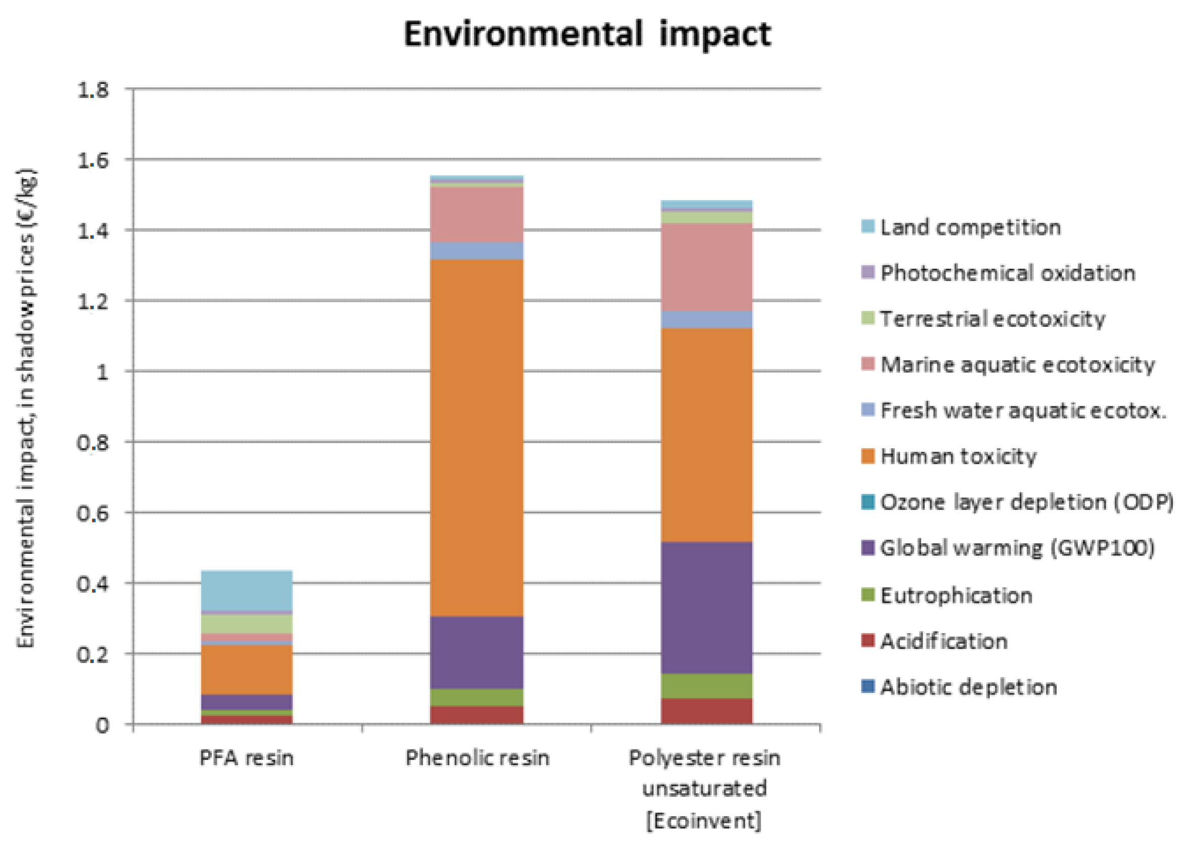
The biobased resin selected for this material is based on poly(furfuryl alcohol) (PFA) from TransFurans Chemicals (TFC). A life-cycle impact assessment was performed by TFC [11], which showed PFA resin has a significantly lower environmental impact than phenolic or polyester resins, with the largest areas of improvement being reduction in global warming potential, ozone layer depletion, human toxicity, and marine aquatic ecotoxicity. Although PFA resin has an environmental impact that is roughly 3× lower than that of the alternatives, its land competition and terrestrial ecotoxicity are notably higher because the material is sourced from an agricultural waste stream. The full list of areas explored in this LCA is shown in Figure 1 below.
To produce PFA resin, furfural is first synthesized from sugarcane bagasse, a waste byproduct that is traditionally burned as biofuel, via a chemical conversion of hemicellulose into furfural. Furfural is then reduced or hydrogenated to form furfuryl alcohol and polymerized to produce PFA in the form of a liquid polymer resin [13]. The curing mechanism for PFA is a condensation reaction driven by an acid catalyst [14]. To tune the viscosity of the resin, a mild catalyst can be used at low temperatures to drive linear chain polymerization until the desired viscosity is reached. The resin can then be fully cured, or cross-linked, by adding more reactive acid catalysts that, when heated to higher temperatures, trigger the formation of methylene bridges and Diels–Alder bonds between the polymer chains [15]. The cross-linking reaction is irreversible and generates moisture as a byproduct as the material cures. When fully cured, PFA exhibits high temperature and chemical resistance, as well as inherent flame retardance [8], which can be further improved using flame-retardant additives. As shown in this study, the uncured resin can be coated onto continuous fibers or woven fabrics to produce prepreg for lamination and bonding applications.
The other materials used for prepreg preparation are standard for contemporary industrial PCB applications. The flame-retardant additive chosen was microencapsulated ammonium polyphosphate (mAPP) from Evonik. This flame retardant comes in the form of ammonium polyphosphate particles, which are manufactured by the microencapsulation of melamine resin [16]. Phosphate-based flame-retardant products are widely considered to be environmentally superior to the bromine-based ingredients that have been broadly used in FR4 boards historically. Ethanol (190 proof) was used to dissolve the PFA resin for the solution coating process. The reinforcement chosen was a 1080-style woven E-glass. The copper used was 0.5 oz electrodeposited copper foil from Denkai America. This copper is an IPC Grade III reliable copper foil with a treated matte side to improve adhesion to substrates [17]. By choosing materials that are typically used in industrial applications, the characteristics of the biobased resin can be better isolated.

2.3. Preparation of Prototypes

2.3.1. Prepreg Preparation

The biobased prepreg AX-3450-1080-50″ RC65 NATURAL (AX-3450, Axiom Materials, Inc., Santa Ana, CA, USA) was produced via solvent impregnation with a target resin content of 65% by weight. This common prepregging method, also used to produce certain FR4s, involves dissolving resin in a solvent, running the fabric through a solvent bath to impregnate the fibers, then heating the prepreg to evaporate the solvent. This process allows for staging of the prepreg during production and results in high levels of impregnation in the fibers.

2.3.2. Monolithic Laminate Fabrication

Monolithic laminates for initial characterization were fabricated using AX-3450. Trials were conducted to determine the ideal cure temperature, and it was determined that curing at 200 °C or above resulted in high void content, cracking, and poor laminate quality, as shown in Figure 2a,b. Thus, 150 °C was chosen as the curing temperature.
Once the curing temperature was determined, additional 4″ × 4″ laminates were cured in a press at 150 °C. These laminates were used to fabricate specimens for the evaluation of the thermal properties. During the development of this curing cycle, it was determined that cooling the laminates under pressure was required to avoid the delamination that occurs due to built-up pressure inside the laminate from condensation, as shown in Figure 2d.
When performing initial thermal testing, the specimens showed evidence that the built-up pressure inside the laminates remained and led to delamination when the material was brought back to elevated temperatures. Consequently, a burp was added to the cure cycle to release the pressure prior to the gel temperature. A burp is performed by releasing pressure and immediately reapplying it, then continuing the curing cycle under pressure. The final curing cycle for fabricating thermal test panels is shown in Table 1, with the burp shown in Step 2. To provide a breathing path for volatiles to escape the laminates in the z-direction, porous polytetrafluoroethylene (PTFE)-coated fabric was applied to either side of the laminate. This proved effective for promoting z-breathing in 4″ × 4″ laminates and in 12″ × 12″ laminates.
For the dynamic mechanical analysis (DMA) and coefficient of thermal expansion CTE thermal tests, specimens of a particular thickness were required. For DMA testing, to avoid any internal pressure in the test specimen, a single ply was cured, as per Table 1, to be tested in a thin-film tension fixture. The CTE testing required a thicker specimen. To achieve the required thickness, a 24-ply laminate that was cured as per Table 1 was machined into four 1″ × 1″ pieces. These were then dried at 100 °C for 24 h to remove any remaining moisture. After drying, the pieces were stacked and bonded together using 2 plies of raw prepreg between each layer. This stack was then re-cured, as per Table 1, resulting in a 0.25″-thick specimen. The results of the thermal analysis are summarized in Section 3.1.2.

2.3.3. Copper Core Fabrication

For the purposes of this paper, the term “copper core” will refer to a composite laminate with copper foil on both sides. Initially, the copper cores of AX-3450 were fabricated by laminating sheets of copper foil on the outer surfaces of 2-ply laminates and were cured as per Table 1. This resulted in the suppression of z-direction breathing, forcing the condensate formed during the curing to be trapped between the laminate surface and the copper foil. This process resulted in blisters, as shown in Figure 3.
Several modifications of the copper core fabrication process were investigated to mitigate blister formation. Improvements to laminate quality were realized by decreasing the ramp rate and dwell time, but blistering was not fully eliminated. As such, the following multi-step process was developed to fabricate blister-free laminates:
  • Fabricate two single-sided copper sub-assemblies;
  • Fabricate one monolithic sub-assembly (i.e., a sub-assembly without copper);
  • Dry all sub-assemblies;
  • Laminate sub-assemblies into final core assembly.
For Step 1, 2 plies of AX-3450 were laminated with copper foil on one side and cured in a press, as per the layup schedule shown in Figure 4 and the curing cycle shown in Table 2. Two of these laminates were fabricated so as to be used as the outer layers of the copper core assembly.
Adding plies to the single-sided sub-assemblies results in blistering of the copper foil. As such, the most reliable means of controlling the thickness of the cores was to include Step 2 of the fabrication process, in which separate monolithic laminates were fabricated with the desired thickness, calculated using the equation below:
Tm = Toverall − 2Tc − nTp
where Tm is the monolithic panel thickness, Toverall is the desired copper core thickness, Tc is the copper foil thickness, Tp is the AX-3450-cured-ply thickness, and n is the number of plies. The monolithic laminates were cured in a press using the layup schedule shown in Figure 5 and the curing cycle shown in Table 2.
In Step 3, once the single-sided and monolithic sub-assemblies were fabricated, they were dried in an air-circulating oven at 100 °C for 24 h. The required drying time was determined by recording the mass measurements of a single-sided sub-assembly, drying at 100 °C over a period of 72 h, and plotting the change in mass over time, as shown in Figure 6a. The laminate mass stabilized after 24 h. To dry the single-sided laminates, a fixture, as shown in Figure 6b, was required to prevent warping due to inconsistencies in thermal expansion between the copper and the composite material. This fixture was assembled using hinges and binder clips; however, other fixturing methods may be used, provided they allow for sufficient air flow to and from the unclad surface of the laminate.
Finally, in Step 4, the dried sub-assemblies were bonded together to fabricate the final assembly via the layup schedule that is shown in Figure 7 and cured as per Table 2. Overall, this multi-step process successfully yielded copper cores with no blistering in the copper foil. Copper cores 12″ × 12″ in size were fabricated using the above method for the tests described in Section 3.2.

2.3.4. Printed Circuit Board Manufacturing and Assembly

The PCB prototypes were manufactured using copper cores fabricated via the multi-step process discussed in Section 2.3.3. The copper cores used for the prototypes were 0.060″ thick and required an 11-ply monolithic sub-assembly. Two copper cores were shipped to a local PCB manufacturer, where they were processed via typical PCB manufacturing processes. These processes include hole drilling, hole plating, photolithography, etching, solder mask application and curing, silk screening, electroless nickel immersion gold (ENIG) plating, and the machining of the PCBs from the panel. ENIG was chosen rather than the hot air solder level (HASL) process because of the material’s sensitivity to the high temperatures used in the HASL process.
At the manufacturing facility, a variety of batch-acceptance tests were run on the panels to ensure compliance with IPC-6012 Cl 3 and IPC-2221. The test parameters for the electrical testing are summarized in Table 3. Microsection testing was also performed. For this test, specimens are machined with a cut through a plated through-hole and cast in an epoxy mold to be observed under a microscope. The microsection testing images from the “As-received” specimens allow for the measurement of the copper cladding and plating thickness, as well as an observation of the quality of the copper pads. Additionally, solder float thermal stress tests were performed on separately machined specimens. These specimens were observed under a microscope for obvious structural damage, such as blistering, delamination, cracking, or damage to copper. Lastly, ENIG plating was measured as per IPC 4552.
During the photolithography, Step 1 of the two panels formed blisters in the copper when the photo-resistive film was applied and cured at 93 °C, as shown in Figure 8. The exposure temperature during this process was far below that which the condensation reaction would initiate (see Section 3.1.2). Hence, the blistering exhibited was presumed to be due to the moisture trapped in the laminate. Such blisters were not visible prior to the photolithography step.
After manufacturing, the boards were forwarded to an assembly house, where they went through a standard surface-mounted technology (SMT) process of solder paste printing and surface-mount device (SMD) component mounting by pick-and-place machines and oven reflow. During oven reflow, the boards reached a maximum temperature of 255 °C. Through-hole and odd-form parts were manually assembled. The solder paste used for assembly was SN63/PB37, but other standard-temperature solder pastes would be acceptable. The printed circuit board assemblies (PCBAs) were then visually inspected following IPC-A-610, a commonly used acceptance standard for electronics assemblies.

3. Results

3.1. Resin, Prepreg, and Monolithic Laminates

3.1.1. Physical Properties

Physical testing on the AX-3450 prepreg was performed using AXIOM internal test procedures (ATS) that were derived from ASTM or SACMA methods. Table 4 shows the physical test results. The prepreg was tested for volatile content, a test used to determine the weight % of volatiles lost when the prepreg is cured. In this case, the volatiles lost in the prepreg can be attributed to the residual solvent left behind from the impregnation process, as well as water lost as a result of the condensation reaction. High volatile content in prepreg can lead to higher void content in cured laminates. The flow test performed is a measurement of the weight % of resin that flows out of the prepreg when cured in a press at 40 psi. If the flow result is too low, the resin between the individual plies is not able to interact, and the result is a laminate that can be easily peeled apart due to poor bonding between the plies. The gel time measurement is used to determine how long the resin remains liquid at the test temperature before hardening. If the gel time is too low, this will impact the flow characteristics and may lead to poor lamination. The prepreg with a zero-tack level had particularly poor adhesion between plies because the resin in the prepreg had advanced beyond gelation and would not melt or flow. This is shown by a low flow result and a gel time of zero seconds. The prepreg with the medium-tack level had favorable adhesion between plies due to the higher flow and gel time results. The resin content test was performed to compare the actual resin content to the target value of 65% by weight.
The higher flow result in the medium-tack prepreg can be seen visually in Figure 9. The photographs were captured using a standard camera. below. The laminate shown in Figure 9b showed consolidation of the plies, resulting in higher laminate quality compared to the zero-tack prepreg, which was able to peel apart at the interface between the plies.

3.1.2. Thermal Properties

The thermal properties of PFA play an important role in the processing of the material. Figure 10 shows a simultaneous differential scanning calorimetry (DSC) and thermogravimetric analysis (TGA) curve tested with a 5 °C/min ramp from room temperature to 600 °C on a cured AX-3450 laminate. The sample shows an increase in heat flow after the glass transition temperature, which is above the original curing temperature. This indicates that the material continues to cure when exposed to a temperature above which the initial reaction occurred. As the temperature increases, the material undergoes a second reaction and continues to react at temperatures as high as 410 °C. As a result of this multi-step reaction, the composite loses 23% of its weight due to the moisture created during the condensation reaction.
A DMA measurement was performed to measure the glass transition temperature via the storage modulus of the material, which indicates the capacity of a material to store energy. To fabricate specimens with no internal pressure for DMA, a single ply of prepreg was cured, as described in Section 2.3.2. This specimen was tested in a thin film fixture with a ramp rate of 5 °C/min from room temperature to 300 °C, with a strain of 0.09% at a frequency of 1 Hz. As shown in Figure 11, the negative slope of the storage modulus before 172 °C occurs due to the slight dissipation of energy as the material loses stiffness and the polymer chains become more mobile with increasing temperature. When the material enters the glass transition, the polymer chain motion increases dramatically, causing the material to soften and lose its ability to store energy, which is shown in DMA data by a sharp decrease in the slope of the storage modulus curve [18]. The Tg of AX-3450, shown by the onset of the change in slope of the storage modulus, occurs at 179.77 °C.
A thermomechanical analysis (TMA) measurement was performed to measure the coefficient of thermal extension (CTE). A specimen 0.25” thick was fabricated, as described in Section 2.3.2. The test was performed with a ramp rate of 10 °C/min from room temperature to 250 °C, per IPC-TM-650 2.4.24. In TMA, the glass transition was shown by an increase in the slope of the change in thickness as the volume of the material began to expand more dramatically due to the increased motion of the polymer chains. To obtain accurate data, a 0.25″ thick specimen was fabricated as per Section 2.3.2 and the curing cycle shown in Table 1. As shown in Figure 12, the Tg of AX-3450 by TMA was 149.6 °C.
The important points to be taken away from the thermal testing performed on AX-3450 are as follows: the cross-linking reaction can be reinitiated when brought above the glass transition. The material, when cured as per Table 1, enters the glass transition in the range of 150–180 °C. The reinitiating of the reaction results in the generation of condensate, which leads to void formation and a loss of the structural integrity of the material. The burp cycle in Table 1 is essential for removing the internal pressure inside the laminate. The CTE of this material is comparable to that of pre-existing FR4 PCB material. The results of the thermal testing are summarized in Table 5.

3.1.3. UL-94 Flammability

The flammability of AX-3450 was tested, as per UL-94, on the monolithic laminates that were fabricated as per Section 2.3.2 with the curing cycle shown in Table 1. The test was performed on specimens as received and conditioned at 70 °C for 7 days per UL-94. In this test, the specimens were oriented vertically and brought in contact with a flame for 10 s. The flame was then removed, and the time required for the specimens to extinguish was measured. All specimens extinguished instantly, with measured values of zero seconds for extinguishing time on both as-received and conditioned specimens. A “V-0” rating is granted for specimens that extinguish within 10 s. Therefore, the AX-3450 material was granted a V-0 rating for flammability. This result shows the superb flammability properties of AX-3450.

3.2. Copper Core Screening

IPC-TM-650 Screening Tests

The copper cores fabricated as per Section 2.3.3 were tested by IPC-TM-650 test methods. The test results are summarized in Table 6 below. The target values were based on a pre-existing high-performance FR4.
The thermal stress specimens were conditioned at 125 °C for 6 h and floated for 10 s on a solder bath at 288 °C. All specimens, both clad and etched, exhibited delamination and blistering, as shown in Figure 13. This was a result of void formation inside the laminate as the reaction was initiated, and condensate was generated in the material at the test temperature of 288 °C. The etched specimens show that the blister formation occurs within the composite itself and not just between the composite and the copper. However, since this test exposes the material to higher thermal stress than any process during PCB manufacture, it was still possible that the prototype boards would be capable of surviving the manufacturing process. To aid in reducing the thermal stress on the prototypes, the electroless nickel immersion gold (ENIG) plating process, which only requires temperatures up to 80 °C, was used instead of the hot air solder level (HASL) process, which requires temperatures up to 255 °C. As a result, the step in the prototyping process that correlated with the highest thermal stress became the solder reflow step during assembly. This step reaches a maximum temperature of 255 °C, the highest the prototype is expected to face during its lifetime. Since this is still considerably lower than the thermal stress test temperature, the assembly process was expected to lead to small-scale void formation but would avoid the degree of blistering observed in the thermal stress specimens.
The water absorption values were significantly higher than the target values. This was likely due to the high void contents in the laminate, which were generated during the final bonding stage of the copper cores. During this stage, the volatiles that were generated no longer had any means of escaping the laminate as the bulk of the laminate was already cured and the outer faces were sealed by copper. Furthermore, the water absorption testing was performed on laminates that had the copper cladding etched off; consequently, any voids that formed between the copper and the AX-3450 at the laminate surface were exposed to the moisture, which led to the diffusion of the water into the laminate. This high water absorption is perhaps the most concerning challenge for the use of PFA in PCBs, as water absorption can affect a variety of material properties that are key to PCB performance, such as resistivity, dielectrics, and continuity.
The volume resistivity values were significantly lower than the target FR4 values. This is believed to be due to the water absorption and generation that occurred in the material. In the case of epoxies, the more water absorbed into the matrix, the less resistant the material will become [19]. Assuming similar effects of moisture on the resistivity in PFA, the high resistivity values at room temperature were a result of the high moisture absorption. Due to dielectric breakdown, the surface resistivity after water absorption was not measurable at room temperature. A decrease in resistivity at elevated temperatures was also observed. While this was expected, it is possible that the conditioning at 125 °C for 24 h also initiated a condensation reaction, thus causing the release of additional moisture within the material.
The peel values in both standard and after thermal stress conditions were roughly half of the target values, while the peel values after fluid exposure were comparable to the target values. These properties were likely affected by the condensation reaction during curing. When the single-sided laminates are cured, the copper-free prepreg face provides an avenue for volatiles to escape; however, once the material is cured, the breathing path for volatiles to escape the laminate is cut off. During the cure of the final assembly, the volatiles closer to the copper face had no means of escaping the laminate and may have built up between the copper and the PFA at a concentration that was high enough to affect the bonding of the copper without forming visible blisters in the foil due to the high pressure on the laminate.
The permittivity values of AX-3450 were within the target values, while the loss tangent values were higher for all of the frequencies other than 10GHz, which is where the values fall into the target range. The permittivity, or dielectric constant, is a measure of the material’s capacity to store electrical energy; thus, a low permittivity is desirable for insulating materials. The permittivity value of AX-3450 decreases with increasing frequency, which is also expected of FR4. The loss tangent, or dissipation factor, is a measure of the amount of current dissipated by the material, meaning that a material with a lower loss tangent will act as a more favorable dielectric material. The loss tangent of AX-3450 was higher than in FR4 in the low-frequency range. However, while the typical loss tangent value of FR4 increased with increasing frequency, the loss tangent of AX-3450 decreased such that it fell within a range comparable to FR4 at 10 GHz. This is evidence that the dielectric properties of AX-3450 improve with increasing frequency in the GHz range.
While the test results did not meet the target values based on a current, high-performance FR4, the tests performed above presented more extreme conditions than the material would experience in a true PCB manufacturing environment. As such, to learn more about the capabilities of AX-3450, PCB prototypes were manufactured using typical manufacturing methods and tested for functionality as per what is described in the next sections.
3.3. Printed Circuit Board Assemblies

3.3.1. PCB Manufacture Batch Acceptance per IPC-6012 Cl 3 and IPC 2221

Two copper cores were sent to a PCB manufacturing facility, where the samples were produced via typical manufacturing methods. The resulting PCBs were tested for conformance to IPC-6012 Class 3 and IPC 2221. Of the 40 boards produced from 2 20-board panel arrays, 52.5% passed electrical testing. Two sets of microsection specimens were cut from each panel for evaluation. The microsection results are summarized in Table 7 below.
Both panels were accepted, despite a void present in the plated through-hole of Panel 2. Typically, this type of feature would lead to the rejection of the panel; however, the size of the void was deemed unlikely to cause shorts or affect board performance. Figure 14 below shows the microsections of the specimens observed.
Figure 14 suggests that the quality of Panel 1 was higher than that of Panel 2, and this is supported by the blistering in the copper of Panel 2 during photolithography. The voids present in Panel 1, while frequent, were smaller and presented less of a risk for the copper or solder to penetrate them. The voids present in Panel 2 were large enough that, had the hole been drilled on top of or next to the large voids to the left or right of the hole, copper or solder could penetrate those voids and potentially connect to a second hole in the board, thus leading to a short in the circuit. Despite the obvious difference in void size between Panel 1 and Panel 2, the 21 boards that passed electrical testing were distributed between the two, with 12 passing from Panel 1 and 9 passing from Panel 2.
The last batch-acceptance tests performed at the PCB manufacturing facility were ENIG plating thickness measurements. The results of this testing are summarized in Table 8 below. This testing showed that the panels complied with the IPC 4552 requirements for ENIG plating.
Based on the batch-acceptance testing performed, both panels were accepted, and the boards that passed electrical testing from each panel were used for the assembly of the final prototypes.

3.3.2. PCB Assembly Batch Acceptance

The assembled boards were inspected and reported to be free of damage and/or defects; thus, they were found to be sufficient for the purposes of a PCB prototype. Aside from the visual inspection of the assembled prototypes, no further testing was performed by the assembler.

4. Discussion

4.1. Advantages of PFA Resin

The primary motivation for this study was to evaluate a biobased material as an alternative to the traditional petrochemical-based FR4 epoxy for its potential in PCB applications. PFA resin was chosen because of its low environmental impact (Figure 1). This resin is sourced from a pre-existing waste stream, which has the potential to drive the composite material toward a net neutral, zero-waste product. Moreover, PFA resin only emits water as a result of the condensation reaction, while other condensation polymerization thermoset systems release hazardous air pollutants (HAPs) such as formaldehyde [20].
For wide adoption, this material must also meet standard FR4 requirements. In this study, AX-3450 has been proven to exhibit excellent flammability characteristics, with the ability to self-extinguish virtually instantly. These properties are favorable for not only PCB applications but also many other applications. The improvement in dielectric properties with increasing frequency in the GHz range is promising for the use of AX-3450 in high-frequency applications. One key positive from this study was the ability to manufacture and assemble prototypes with existing manufacturing techniques. With improvements to the void content and moisture absorption, the material shows potential for use in PCB applications.

4.2. Challenges with PFA Resin

While PFA-based prepregs show potential compared to previous attempts at biobased prepregs, there are still several challenges to overcome that are related to PFA for it to be used in PCB applications. The fundamental challenge with this resin system is the condensation reaction during curing. This reaction mechanism is the root cause of high void content in the laminate, which leads to increased water absorption. This directly influences several material characteristics that are important for PCB applications, including resistivity and dielectric properties. Higher moisture content leads to lower resistivity, higher permittivity, and higher loss tangent values. Moreover, the bonding surface between the copper and the PFA may be affected by moisture absorption and generation during curing, which contributes to the peel performance and the blistering observed in the copper throughout the copper core and PCB manufacturing processes. Consequently, the condensation reaction and moisture absorption have a direct effect on the 52% passing rate in electrical testing of the unassembled PCB prototypes, which presents a clear disadvantage compared to existing PCB substrates.
Other manufacturing process challenges will require additional optimization. For example, the current PFA resin formulation cannot be staged to zero tack in the same manner as epoxy-based FR4 can. This higher-tack prepreg reduces handleability during lamination, which may hinder downstream applications and the widespread adoption of the prepreg.

4.3. Areas of Improvement

If the reaction mechanism can be addressed, and chemistry can be developed that reduces volatile generation or removes it altogether by targeting an additional reaction mechanism, the potential for the use of PFA in PCBs becomes much more realistic. To target an addition reaction, the chemistry of the resin must be drastically altered.
Significant improvements to the overall biobased content of the system can be made if biobased fibers can be sourced or developed with similar dielectric properties as E-glass. A fully biobased composite could greatly improve sustainability and reduce this material’s contribution to E-waste. Further, the development of a biobased woven fabric could significantly contribute to the processability and scalability of a biobased prepreg system. It is imperative in this scenario that the essential properties such as dielectrics, resistivity, and water absorption be tested as a change in fabric can greatly impact these properties.

4.4. Future Applications

Future applications of PFA-based composites include low-flammability applications and other applications that commonly use phenolic systems (as PFA has been shown to have many similarities to phenolics). The condensation reaction mechanism of both materials leads to similar processing challenges that require techniques to remove the volatiles during curing in order to avoid void formation. The similarity of PFA to phenolic systems shows potential for its use in the same range of applications. Moreover, PFA has a distinct advantage over phenolic materials when it comes to hazardous air pollutant (HAP) and volatile organic compound (VOC) generation, which is a key concern surrounding the current use of phenolic systems [20]. The applications in which PFA systems may be viable include low-flammability and low-heat-release applications such as aircraft and aerospace, as well as in railway and construction applications.

5. Conclusions

The purpose of this study was to evaluate a poly(furfuryl alcohol)(PFA)-based prepreg for its potential in PCB applications. This composite system poses some advantages, such as superb flammability and superior environmental features. However, the chemistry creates challenges for the preparation of PCB laminates due to the condensation reaction mechanism, as it requires special processes to manufacture double-sided copper cores for multilayered boards. Once this process was developed, the manufacturing of PCB prototypes showed compatibility with typical PCB manufacturing processes, as well as with assembly processes. The overall yield of boards passing electrical testing was roughly half, with the primary reason being the high void content in the matrix of the copper cores, which led to poor water absorption. Overall, the PFA-based prepreg shows potential for PCB applications, although the low reliability would need to be addressed before this system could be integrated into commercial electronics.

Author Contributions

Conceptualization, B.H.N., A.T. and J.D.L.; validation, A.M.C., J.V. and A.T.; investigation, A.M.C.; data curation, A.M.C. and J.V.; writing—original draft preparation, A.M.C.; writing—review and editing, all authors; visualization, A.M.C.; project administration, J.V.; funding acquisition, B.H.N. All authors have read and agreed to the published version of the manuscript.

Funding

This work was funded internally by the participating companies.

Data Availability Statement

The data presented in this study are available on request from the corresponding authors. The data are not publicly available due to privacy restrictions.

Acknowledgments

The Microsoft Corporation would like to acknowledge Rizwan FaZil, Karin Strauss, Paul Kos, and Winston Saunders for their contributions. Axiom Materials would like to acknowledge Bill Webb of Axiom Materials and Hans Hoydonckx of TransFurans Chemicals for their contributions.

Conflicts of Interest

All the authors with “[email protected]” emails were employed by Axiom Materials, Inc. throughout the duration of this work. All authors with “[email protected]” emails were employed by the Microsoft Corporation during the duration of this work. The authors declare that the research was conducted in the absence of any commercial or financial relationships that could be construed as a potential conflict of interest.

References

  1. Madkhali, H.; Duraib, S.; Nguyen, L.; Prasad, M.; Sharma, M.; Joshi, S. A Comprehensive Review on E-Waste Management Strategies and Prediction Methods: A Saudi Arabia Perspective. Knowledge 2023, 3, 163–179. [Google Scholar] [CrossRef]
  2. Nassajfar, M.N.; Deviatkin, I.; Leminen, V.; Horttanainen, M. Alternative Materials for Printed Circuit Board Production: An Environmental Perspective. Sustainability 2021, 13, 12126. [Google Scholar] [CrossRef]
  3. Kovacs, B.; Geczy, A.; Horvath, G.; Hajdu, I.; Gal, L. Advances in Producing Functional Circuits on Biodegradable PCBs. Period. Polytech. Electr. Eng. Comput. Sci. 2016, 60, 223–231. [Google Scholar]
  4. Zhan, M.; Wool, R. Design and evaluation of bio-based composites for printed circuit board application. Compos. Part A 2012, 47, 22–30. [Google Scholar] [CrossRef]
  5. Kosbar, L.L.; Gelorme, J. Biobased epoxy resins for computer components and printed wiring boards. In Proceedings of the 1997 IEEE International Symposium on Electronics and the Environment, San Francisco, CA, USA, 5–7 May 2017; pp. 28–32. [Google Scholar]
  6. Lincoln, J.D.; Shapiro, A.A.; Earthman, J.C.; Saphores, J.M.; Oguseitan, O.A. Design and Evaluation of Bioepoxy-flax Composites for Printed Circuit Boards. IEEE Trans. Electron. Packag. Manuf. 2008, 31, 211–220. [Google Scholar] [CrossRef]
  7. Chang, B.P.; Mohanty, A.K.; Misra, M. Studies on durability of sustainable biobased composites: A review. RSC Adv. 2020, 10, 17955. [Google Scholar] [CrossRef] [PubMed]
  8. Deka, H.; Misra, M.; Mohanty, A. Renewable resource based “all green composites” from kenaf biofiber and poly(furfuryl alcohol) bioresin. Ind. Crops Prod. 2012, 41, 94–101. [Google Scholar] [CrossRef]
  9. Accurate Plastics. Acculam® Epoxyglas G10/FR4 Product Data Sheet. Available online: http://www.acculam.com/Product/EpoxyglasG10FR4 (accessed on 3 October 2022).
  10. Cylex® Engineering Plastics Limited. Typical Properties Data Sheet of FR4. Available online: http://www.cylexplastics.co.uk (accessed on 3 October 2022).
  11. Hoydonckx, H.; Keijzer, E.E. Updated Results Resin Analysis (TFC). Unpublished manuscript, last modified 5 May, 2014.
  12. Hoydonckx, H. Use of LCA Data. Unpublished memo, last modified 11 November, 2023.
  13. Kumar, R.; Anandjiwala, R.D. Alternative fuels from waste cellulosic substrates and poly furfuryl alcohol. Fuel 2012, 93, 703–705. [Google Scholar] [CrossRef]
  14. Kumar, R.; Anandjiwala, R. Process for Preparing Polyfurfuryl Alcohol Products. WIPO Patent Application WO 2012/123902, 20 September 2012. [Google Scholar]
  15. Tondi, G.; Cefarin, N.; Sepperer, T.; D’Amico, F.; Berger, R.J.F.; Musso, M.; Birarda, G.; Reyer, A.; Schnabel, T.; Vaccari, L. Understanding the Polymerization of Polyfurfuryl Alcohol: Ring Opening and Diels-Alder Reactions. Polymers 2019, 11, 2126. [Google Scholar] [CrossRef] [PubMed]
  16. Clariant. Exolit® AP 462. Available online: http://www.clariant.com (accessed on 5 October 2022).
  17. Denkai America. Technical Data Sheet TOB-III. Available online: Denkaiamerica.com/wp-content/uploads/2021/02/03-Denkai-Tech-Data-Sheet-TOB-III-updated-2.2.21.pdf (accessed on 7 September 2022).
  18. Xia, X.; Li, J.; Zhang, J.; Weng, G.J. Uncovering the glass-transition temperature and temperature-dependent storage modulus of graphene-polymer nanocomposites through irreversible thermodynamic processes. Int. J. Eng. Sci. 2021, 158, 103411. [Google Scholar] [CrossRef]
  19. Ciprian, R.; Lehman, B. Modeling effects of relative humidity, moisture, and extreme environmental condition on power electronic performance. In Proceedings of the 2009 IEEE Energy Conversion Congress and Exposition, San Jose, CA, USA, 20–24 September 2009; pp. 1053–1059. [Google Scholar]
  20. Sadler, J.M.; Yeh, I.; Toulan, F.R.; McAninch, I.M.; Rinderspacher, B.C.; La Scala, J.J. Kinetics studies and characterization of poly(furfuryl alcohol) for use as bio-based furan novolacs. J. Appl. Polym. Sci. 2018, 135, 46608. [Google Scholar] [CrossRef]
Figure 1. Environmental impact of 1 kg of PFA resin compared to phenolic and polyester resins, calculated with the CML2 shadow price method [11]. Reprinted with permission from Ref. [12]. 2023, Hans Hoyndonckx.
Electronics 12 04729 g001
Figure 2. Cross-section of AX-3450 laminates cured at (a) 250 °C, (b) 200 °C, (c) 150 °C, and (d) 150 °C, removed hot and resulting in delamination. High curing temps result in cracking and void formation due to the condensate formed throughout curing. The images were captured using a handheld USB digital microscope. Scale bars are 0.5 mm in length.
Electronics 12 04729 g002
Figure 3. Top view of a 2-ply, 12″ × 12″ trial laminate that was cured as per Table 1 with copper on both sides. The ~1” blisters are visible. The photograph was captured using a standard camera. The scale bar is 2″.
Electronics 12 04729 g003
Figure 4. Layup schedule for Step 1—single-sided copper sub-assembly.
Electronics 12 04729 g004
Figure 5. Layup schedule for Step 2—monolithic sub-assembly. The number of AX-3450 plies was adjusted to achieve the desired thickness.
Electronics 12 04729 g005
Figure 6. Drying of single-sided copper sub-assemblies in Step 3. (a) Plot of the change in mass of two sub-assemblies over time when dried at 100 °C. (b) Photograph of the drying fixture used to prevent warping. The photograph was captured using a standard camera. The scale bar is 2′′.
Electronics 12 04729 g006
Figure 7. Layup schedule for Step 4—final copper- core assembly.
Electronics 12 04729 g007
Figure 8. Photograph of a panel after machining and photolithography. Blisters formed in the copper after exposure to 93 °C during photolithography. The photograph was captured using a standard camera. The scale bar is 2″.
Electronics 12 04729 g008
Figure 9. Photographs of the 4″ × 4″ flow specimens for the (a) zero- tack prepreg and (b) medium-tack prepreg. The photographs were captured using a standard camera.
Electronics 12 04729 g009
Figure 10. Simultaneous DSC/TGA cured up to 600 °C. The red lines represent the limits used to calculate the area under the Heat Flow curve to generate the ▲H values shown in J/g.
Electronics 12 04729 g010
Figure 11. DMA data on 1-ply laminate that was cured as per Table 1.
Electronics 12 04729 g011
Figure 12. Tg by TMA data on a 0.25″-thick specimen.
Electronics 12 04729 g012
Figure 13. Blistering and delamination in clad (left) and unclad (right) thermal stress specimens. The photograph was captured using a standard camera. The scale bar is 1″.
Electronics 12 04729 g013
Figure 14. This figure shows the microsections of the specimens used for the microsection testing: (a) Panel 1, as received; (b) Panel 1, after thermal stress; (c) Panel 2, as received (the void present in the plated through-hole that caused the “Reject” value for Panel 2 in the microsection report can be seen in this image); and (d) Panel 2, after thermal stress. These images were captured using a digital microscope. Scale bars are 0.5 mm in length.
Electronics 12 04729 g014
Table 1. This table shows the modified curing cycle for larger-area monolithic laminates.
Press SetpointStep 1Step 2Step 3Step 4Step 5
Temperature (°C)10010015015025
Dwell Time (min)N/A0N/A90N/A
Ramp Rate (°C/min)2.2N/A2.2N/A<1 1
Pressure on Laminate (psi) 750400400400
1 Cooling ramp rate not controlled and subject to the natural rate of the press.
Table 2. This table shows the cure cycle used for the copper core sub-assembly and final assembly. It includes burping in Step 2 and a decreased ramp rate and dwell time when compared to Table 1.
Press SetpointStep 1Step 2Step 3Step 4Step 5
Temperature (°C)10010015015025
Dwell Time (min)N/A0N/A75N/A
Ramp Rate (°C/min)1.1N/A1.1N/A<1 1
Pressure on Laminate (psi) 750400400400
1 Cooling ramp rate not controlled subject to the natural rate of the press.
Table 3. This table summarizes the parameters used for the electrical batch-acceptance testing performed after PCB manufacturing on the copper cores made from AX-3450.
Test Parameters
MethodResistive per IPC-9252
Isolation Resistance10 MΩ
Continuity Resistance10 Ω
Source DataNet List
Test Equipment UsedMicrocraft (Flying Probe)
Test Voltage150 Volts
Table 4. Physical test results of the AX-3450 prepregs.
Tack TargetTest PerformedTest MethodTest Temp (°F)Result
Dry/0Tack TestATS-015A73Dry/0
Volatile Content @ 10 min (%)ATS-0022754.542
Gel Time (s)ATS-0032750
Resin Flow @ 40 psi (%)ATS-0042751.442
Resin Content (%)ATS-0057367.859
Medium/3Tack TestATS-015A73Medium/3
Volatile Content @ 10 min (%)ATS-0022754.838
Gel Time (s)ATS-00327535
Resin Flow @ 40 psi (%)ATS-0042753.817
Resin Content (%)ATS-0057369.888
Table 5. This table summarizes the thermal testing performed on the AX-3450 laminates. The testing was performed under IPC-TM-650 test methods unless otherwise stated.
Test PerformedTest MethodTest ConditionTest ResultUnitsTarget Value *
TgATS-50 Rev ADSC175.0°C170–200
2.4.24.2DMA179.8°C-
2.4.24.3TMA149.6°C-
CTE, Z-axis2.4.24Alpha 1, TMA67.5PPM/°C45
Alpha 2, TMA235.2PPM/°C230
CTE, X-, Y-axes2.4.24Pre-Tg, TMA17.7/20.2PPM/°C13/14
* Target values are based on the properties of a commercial FR4 material that is commonly used in the PCB industry.
Table 6. This table summarizes the IPC-TM-650 screening test results on copper cores with 0.5 oz copper foil that were fabricated as per Section 2.3.3 and cured as per Table 2.
Test PerformedTest MethodTest ConditionTest ResultUnitsTarget Value *
Thermal StressIPC-TM-650 2.4.13.1CladFailRatingPass Visual
EtchedFailRatingPass Visual
Water AbsorptionIPC-TM-650 2.6.2.1E-1/105 + D-24/232.18%<0.15
Peel Strength, As ReceivedIPC-TM-650
2.4.8
Average2.7lb/in>4.5
Peel Strength, After Thermal StressAverage2.6lb/in>4.5
Peel Strength, After Fluid ExposureAverage2.9lb/in>3.0
Volume ResistivityIPC-TM-650 2.5.17.1C-96/35/909.2 × 102MΩ-cm>1.0 × 10⁶
E-24/1251.5 × 102MΩ-cm>1.0 × 10³
Surface ResistivityIPC-TM-650 2.5.17.1C-96/30/90N/AMΩ>1.0 × 104
E-24/1254.0 × 103MΩ>1.0 × 10³
Permittivity, MHz RangeIPC-TM-650 2.5.5.11 MHz5.8-<5.5
Permittivity, GHz rangeIEC 61189-2-721:20151.1 GHz5.0-<5.4
2.5 GHz5.0-<5.4
5 GHz4.7-<5.4
10 GHz4.1-<5.4
Loss Tangent, MHz RangeIPC-TM-650 2.5.5.11 MHz0.082-<0.04
Loss Tangent, GHz RangeIEC 61189-2-721:20151.1 GHz0.090-<0.035
2.5 GHz0.087-<0.035
5 GHz0.066-<0.035
10 GHz0.025-<0.035
* Target values are based on the properties of commercial FR4 material.
Table 7. This table summarizes the microsection report for batch-acceptance testing performed on the PCBs manufactured from the copper cores of AX-3450. Each test was given a value of “Accept” or “Reject” based on its conformance to IPC-6012 Class 3 requirements. Any numerical value refers to the thickness of the feature observed in mm.
Test ConditionFeature ObservedPanel 1Panel 2
As ReceivedHole Copper Plating0.03 0.03
Surface Copper Plating0.030.03
Surface Cladding0.030.03
Tin/Lead PlatingAcceptAccept
Min. Annular RingAcceptAccept
Lifted LandsAcceptAccept
Minimum Dielectric ThicknessAcceptAccept
Surface SolderabilityAcceptAccept
Hole SolderabilityAcceptAccept
Final DesignationAcceptAccept
After Thermal StressBlistering or DelaminationAcceptAccept
Plated Through-Hole AcceptAccept
Copper CrackingAcceptAccept
SeparationAcceptAccept
Laminate Voids > 0.003″AcceptReject *
Lifted Lands AcceptAccept
* Panel 2 had a laminate void inside its plated through-hole.
Table 8. ENIG plating thickness results with respect to the requirements of IPC 4552.
StatisticsAu Plating (µm)NiP Plating (µm)
Min. Requirement0.040 3.00
Max. Requirement0.100 5.99
Mean Value0.054 4.35
Range0.0041 0.052
Min. Measured0.052 4.33
Max. Measured0.056 4.38
Std. Dev.0.00150.021
Pct. (%) Dev.2.880.48
Disclaimer/Publisher’s Note: The statements, opinions and data contained in all publications are solely those of the individual author(s) and contributor(s) and not of MDPI and/or the editor(s). MDPI and/or the editor(s) disclaim responsibility for any injury to people or property resulting from any ideas, methods, instructions or products referred to in the content.