Article

The Influence of the Skin Phenomenon on the Impedance of Thin Conductive Layers

by
Stanisław Pawłowski
1,
Jolanta Plewako
2,
Ewa Korzeniewska
3,* and
Dariusz Sobczyński
2
1
Department of Electrodynamics and Electrical Machine Systems, Faculty of Electrical and Computer Engineering, Rzeszow University of Technology, Pola 2, 35-959 Rzeszow, Poland
2
Department of Power Electronics and Power Engineering, Faculty of Electrical and Computer Engineering, Rzeszow University of Technology, Pola 2, 35-959 Rzeszow, Poland
3
Institute of Electrical Engineering Systems, Faculty of Electrical Engineering, Electronics, Computer and Control Engineering, Lodz University of Technology, Stefanowskiego 18, 90-537 Lodz, Poland
*
Author to whom correspondence should be addressed.
Electronics 2023, 12(23), 4834; https://doi.org/10.3390/electronics12234834
Submission received: 25 October 2023 / Revised: 23 November 2023 / Accepted: 27 November 2023 / Published: 30 November 2023
(This article belongs to the Special Issue Modern Computer Vision and Image Analysis)

Abstract

:
This paper analyzes the influence of the skin effect and the proximity effect on the inductance and impedance of thin conductive layers. The motivation for taking up this topic is the initial assessment of the possibility of using conductive layers deposited with the PVD technique on textile materials as strip or planar transmission lines of high-frequency signals (e.g., for transmitting images). This work pursues two goals. The first of them is to develop and test a numerical procedure for calculating the electromagnetic field distribution in this type of issue, based on the fundamental solution method (FSM). The second aim is to examine the impact of the skin phenomenon on the resistance, inductance and impedance of thin conductive paths. The correctness and effectiveness of FSM for the analysis of harmonics of electromagnetic fields in systems containing thin conductive layers were confirmed. Based on the performed simulations, it was found that in the frequency range above 10 MHz, the dependence of resistance and impedance on frequency is a power function with an exponent independent of the path width. Moreover, it was found that for paths with a width at least several times greater than their thickness, the dependence of the phase shift between current and voltage on frequency practically does not depend on the path width.

1. Introduction

Wearable electronics is currently one of the rapidly developing fields combining the issues of computer science, electronics, materials science and telecommunications. Striving to miniaturize electronic components used in this industry, there is a need to produce thin-film components that act as active or passive components such as capacitors, resistors, transistors, diodes or photodetectors. Such elements can also be used to transmit high-frequency signals as a transmission medium that enables data transmission without interference in telecommunications systems.
One example of the use of thin electrically conductive layers for the transmission of high-frequency signals is the RFID (Radio Frequency Identification) technology [1,2]. In this technology, these structures are used as antennae or induction coils that receive and transmit radio signals to RFID readers. Those types of structures can also be used as the active part of sensors for pathogens detection [3]. Taking into account the developing 5G and 6G technology, such structures will also be used for data transmission, e.g., in smart healthcare and industrial manufacturing [4,5,6]. According to reports from the Huawei 6G research team [7], research is being conducted on integrated sensing and communications with optical wireless (ISAC-OW) technology to develop solutions such as holographic hospitals and industrial automation.
Electroconductive thin films can be produced via various methods, such as physical vacuum deposition (PVD) [8,9], chemical vapor deposition (CVD) [10], electrochemical deposition [11], spin-coating [12], sol–gel technology [13,14,15], magnetron sputtering [16], ink-jet printing [17,18], screen printing [19] or electrospinning [20]. The development of new applications based on flexible and wearable devices with large surface areas requires thin-film electronics that can be fabricated using solvent methods. Lin et al. conducted research on preparing the nanosheet inks and their scalable assembly into van der Waals thin films and devices [21]. The choice of the method depends on the type of deposited conductive material, substrate, physical and chemical properties of the thin layer, as well as the cost and scale of production.
The physical vapor deposition method of creating thin films has several advantages. It allows for the deposition of high-quality films consisting of metals, alloys, ceramics and semiconductors with excellent adhesion and uniformity. The process enables the control of film thickness at an atomic level, resulting in precise and consistent film properties. It offers the flexibility to create thin films with different compositions and structures, making it suitable for various applications. Thanks to relatively high deposition rates compared to other methods, the PVD technique is scalable, allowing for easy upscaling from laboratory-scale to large-scale production, so it is suitable for large-scale production applications and reduces processing time. Additionally, it is a dry process that operates in a high-vacuum environment, minimizing material waste and contamination. It reduces the need for additional chemical processing and eliminates the use of solvents. Using technological masks or modifying the shape with the use of a laser beam [22], it is possible to create patterned thin films or modify the film properties selectively. The quality of the layers produced can be assessed using optical computed tomography [23] with higher resolution than another type of tomography [24].
Thin electroconductive layers can be applied to various substrates, such as paper, plastic, metal or fabric. In the case of fabrics, the thin-film structures produced are characterized by greater flexibility, which allows their use in wearable electronics combined with clothing.
Considering the use of such structures in alternating current circuits, it is advisable to analyze the presence of skin and proximity effects in them.
Skin and proximity effects are important for the transmission of high-frequency signals, such as radio waves, microwaves or fiber optics. According to a well-known theory, the depth of penetration of a magnetic field or current into a conductor depends on the current frequency, resistivity and magnetic permeability of the medium [25]. The higher the frequency, the smaller the penetration depth and the greater the skin effect, which affects the electrical properties of structures. The proximity effect can affect the signal quality, frequency response, characteristic impedance and reflection coefficient of the transmission line. To minimize it, various techniques are used in the design and construction of transmission lines, such as using transmission lines with a symmetrical geometry, such as a two-wire line or a symmetrical line, which reduces the interaction of magnetic fields, or using transmission lines with an asymmetric geometry, such as a microstrip line or a strip line, which reduces the magnetic field induction by the substrate. It is also possible to use conductors of small diameter or thickness, which reduces the depth of magnetic field penetration and increases the homogeneity of the current distribution [26].
In the case of thin textronic electroconductive structures, the thickness of the conductor layer is less than 0.5 mm. The analysis of those type of effects in conductors is a known issue; however, the analysis of their occurrence in thin textronic layers is a new issue, which is undertaken by the authors of this study.
The peculiarity of conductive textronic layers compared to others found in electronic devices (e.g., printed circuit paths) is that their surfaces are not flat because they take a shape similar to the texture of a textile material, and they also contain microdefects. It turns out that these features have a significant impact on the conductive properties of such layers [8]. For this reason, the assessment of conductive parameters of textronic layers, such as resistance, inductance or capacitance, requires the use of quite complex field calculations. Due to the complex issues of field distribution inside the electroconductive path, one of the simplifications adopted in this article is the homogeneous structure of the produced layer. In further work, the authors plan to expand the model and analyze the impact of occurring defects on its electrical parameters in the case of high-frequency current, similar to the work on a constant signal [8].
The first goal of this work is to implement and test the fundamental solution method (FSM), which is rarely used in the analysis of electromagnetic fields, for those type of problems. Compared to other finite difference and finite element methods most frequently used in field problems, FSM has several advantages [27]:
  • As a boundary method, it does not require discretization of the interiors of the areas considered in the system, but only of their edges, which ultimately leads to significantly smaller numerical models, as exemplified by the 3D SET simulator described in [28];
  • Gives a solution in an analytical form that strictly satisfies a given differential equation; the approximation concerns only the fulfillment of the boundary conditions;
  • Does not create additional difficulties when analyzing fields in open areas;
  • Enables relatively easy estimation of the numerical error of the solution and obtaining more and more accurate solutions in subsequent iteration steps.
A comparison of the effectiveness of FSM with the finite element method (FEM) implemented using the commercial ANSYS Electromagnetic Suite 18.2 package in electrostatics issues can be found in [29].
The second goal of the work is to investigate, using field analysis, the impact of the skin phenomenon on the transport properties of thin conducting paths with sinusoidally variable current depending on the dimensions of the path and the current frequency.

2. Formulating the Issue

A thin conductive layer can be defined as a conductive path whose thickness is much smaller than its width. In terms of the skin effect, a thin layer could be defined as one whose thickness is much smaller than the equivalent field penetration depth, because then the effects of changes in the electromagnetic field in the direction perpendicular to its surface and for computational purposes treat it even as infinitely thin. However, such a definition depends on the field frequency and material parameters of the path (e.g., at a frequency of 50 Hz, a 1 mm thick copper layer can be treated as thin, but at a frequency of 10 kHz it cannot).
The subject of consideration is the electromagnetic field generated by a sinusoidally alternating electric current flowing in an infinitely long, straight path with an oval cross-section, immersed in a uniform dielectric region. The geometry of the model with the adopted coordinate system and the symbols used later are illustrated in Figure 1.
The shape of the side edges of the path in the form of cylindrical surfaces was adopted for the following reasons:
  • This way, computational complications caused by geometric peculiarities that appear in the case of a rectangular cross-section path (sharp edges) are avoided;
  • Assuming a = 0 in the model in Figure 1, the cross-section of the path becomes a circle, which makes it possible to verify the correctness of numerical calculations by comparing them with a known analytical solution;
  • It was found that due to the very small thickness of the layers sputtered with PVD technology compared to their other dimensions, this shape should not have a significant impact on their conductive properties.
The following physical assumptions were made:
  • Material parameters μ, ε, γ of both areas of the system are constant;
  • The current density vector is parallel to the wire axis (OZ) and varies sinusoidally in time;
  • Maxwell shift currents in the conducting area ΩII are negligibly small;
  • There are no unbalanced electric charges in the system.
In order to mathematically formulate the problem in both areas, the complex vector potential A defined by the relations is introduced:
B = rot A , div A = 0 .
where B is the complex amplitude of magnetic induction. Knowledge of the vector potential also allows to determine the complex amplitude of the electric field intensity E:
E = j ω A .
With the adopted assumptions, the only non-zero component of the vector potential is the component parallel to the OZ axis, which satisfies the Helmholtz equation [30] in the areas ΩI, ΩII:
Δ A = Γ 2 A ,
where  Γ = ω μ 1 ε 1  in area ΩI, and  Γ = j ω γ 2 μ 2  in area ΩII.
According to the classical boundary conditions of electrodynamics, on the surface S, the tangential components of the electric field strength vectors E and magnetic field H are continuous, which, in relation to (1) and (2), means that
A I = A II ,
μ r A I n = A II n ,
where  μ r = μ 2 / μ 1  AI, AII are the limit values of the function A on the surface S, calculated from the side of the area ΩI and ΩII, respectively.
The issue comes down to searching for functions AI and AII that satisfy Equation (3) and boundary conditions (4) and (5) on the boundary surface S in the areas ΩI and ΩII.

3. Solution Method

In order to solve the described issue, the fundamental solution method (FSM) was used. The sought vector potential functions are presented in the following form:
A I ( x , y ) = A 0 ( x , y ) + i = 1 N q i I F i I x , y , ( x , y ) Ω I ,
A II ( x , y ) = i = 1 N q i II F i II x , y , ( x , y ) Ω II ,
where:
A0 = primary field potential;
F i I = H 0 ( 2 ) Γ ( x x i ) 2 + ( y y i ) 2 —fundamental solutions of Equation (3) in the area ΩI,
F i II = K 0 Γ ( x x i ) 2 + ( y y i ) 2 —fundamental solutions of Equation (3) in the area ΩII
H 0 ( 2 )  = Hankel function of the second kind,
K 0  = modified Bessel function of the second kind,
q i I ,   q i II  = coefficients of approximation sums determined on the basis of boundary conditions (4) and (5).
The singular points  ( x i , y i )  of fundamental solutions (“fictional sources”) are determined outside the area in which a given solution is valid, i.e., for the solution  ( x i , y i ) Ω II ( x i , y i ) Ω II  for  F i I  solution and  ( x i , y i ) Ω I  for  F i II  solution (Figure 2).
The A0 field, which serves as a “zero” approximation of the formulated problem, is the field originating from the current of constant linear density flowing on the surface S0 { x a , y = 0 } in the direction parallel to the OZ axis. Such a solution can be obtained by integrating the solution of Equation (3) in the region ΩI for an infinitely thin straight wire. In such a case, the system is characterized by axial symmetry and Equation (3) in cylindrical coordinates takes the form of a modified Bessel equation, the solution of which can be written as follows:
A ( r ) = j μ 1 i 4 π   H 0 ( 2 ) ( Γ r ) , r = x x 0 2 + y 2 .
The vector potential of the field originating from the uniformly distributed current flowing on the surface S0 is obtained by integrating (8) with respect to x0:
A 0 ( x , y ) = j μ 1 i 0 4 π   a a H 0 ( 2 ) Γ x x 0 2 + y 2 d x 0 .
The integral occurring in (9) generally requires numerical solution, but in the close zone (i.e., for Γr << 1, i.e., at a distance significantly smaller than the length of the electromagnetic wave emitted by the current flowing in the path), the approximation of the H0 function can be used for small arguments [31]:
  H 0 ( 2 ) ( Γ r ) j 2 π ln Γ r , Γ r < < 1 .
In this case, the integral (9) can be calculated analytically and the result is as follows:
A 0 ( x , y ) = μ 1 i 0 2 π   x ln R 1 R 2 a ln R 1 R 2 a 2 y atan x + a y atan x a y   ,   x ,   y Ω I
where:
R 1 = x a 2 + y 2 , R 2 = x + a 2 + y 2 .
The formulae for the derivatives of the A0 potential need to determine the components of magnetic induction and to calculate the normal derivative occurring in condition (5). In the general case:
A 0 x = j μ 1 i 0 4 π Γ   a a x x 0 x x 0 2 + y 2 H 1 ( 2 ) Γ x x 0 2 + y 2 d x 0 ,
A 0 y = j μ 1 i 0 4 π Γ   a a y x x 0 2 + y 2 H 1 ( 2 ) Γ x x 0 2 + y 2 d x 0 .
In the case Γr << 1:
A 0 x = μ 1 i 0 4 π ln ( x a ) 2 + y 2 ( x + a ) 2 + y 2 ,
A 0 y = μ 1 i 0 2 π atan x a y atan x + a y   .
The functions which are defined by Formulae (6) and (7) satisfy Equation (3) exactly. The coefficients  q i I ,   q i II  are determined postulating that (6) and (7) satisfy the boundary conditions (4) and (5) at points (xk, yk), k = 1, …, N on the boundary surface S distributed approximately evenly (with a possible higher density on parts rounded and in their close vicinity, where less regularity of function A or its derivatives should be expected). As a result, this leads to a linear system of equations of order 2N:
i = 1 N F i , k I q i I i = 1 N F i , k II q i II = A 0 , k , k = 1 , , N ,
i = 1 N G i , k I q i I i = 1 N G i , k II q i II = G 0 , k , k = 1 , , N ,
where:
F i , k I ,   II = F i I ,   II ( x k , y k ) , A 0 , k = A 0 ( x k , y k ) , ( x k , y k ) S ,
G i , k I = μ r s k , x F i I y s k , y F i I x x = x k ,   y = y k ,
G i , k II = s k , x F i II y s k , y F i II x x = x k ,   y = y k ,
G 0 , k = s k , x A 0 y s k , y A 0 x x = x k ,   y = y k .
s k , x s k , y —coordinates of the sk vector tangent to the surface S at the point (xk, yk).
After numerically solving the system (17) and (18) and substituting  q i I ,   q i II  into (6) and (7), the desired solution is obtained.
The components of the electromagnetic field are determined based on the Equations (1) and (2), from which other interesting quantities can then be calculated:
Complex current density amplitude:
  J = γ E ;
Complex current amplitude:
I m = S c J d s ;
Active and reactive power per unit length of the conductive path:
  P = 1 γ S J 2 d S , Q = ω μ S B 2 d S ;
And resistance, internal inductive reactance and impedance:
R = 2 P I m 2 , X L = 2 Q I m 2 .
The integration area Sc in Formulae (20) and (21) means the cross-sectional area of the path.

4. Calculation Results

In order to numerically implement the method described in the previous chapter, the authors decided to create the new software. The use of Fortran (Intel Parallel Studio XE Composer Edition for Fortran Windows) or C++ (Dev-C++) allows for effective management of available computer hardware resources as well as full control over the accuracy of the obtained results. It was described in the works [32,33], where the authors have a similar approach to solving scientific problems, as well as our previous publications [34]. Based on the presented formulae, a numerical program was prepared to calculate the distribution of the electromagnetic field and the current density flow field in the conductive path and its impedance Z.
Example results of calculations of the electric field and magnetic induction components are shown in Figure 3. These results confirm the correctness of the method in terms of meeting the boundary conditions regarding the continuity of the appropriate components of the electromagnetic field on the boundary surface S of areas ΩI, ΩII. Because these solutions result from the exact solutions of Equation (3), it means that the results obtained are also correct solutions to the formulated problem.
Figure 4 shows the current density distributions on the cross-section of a path with the same parameters as above, at different current frequencies. They illustrate the influence of the skin effect on the current density distribution in the tested model. At frequencies not exceeding 10 kHz, the calculated current density distribution for such path parameters is practically uniform. Above this frequency, a current displacement effect is observed from the center of the path to its side edges, i.e., in the direction parallel to the path surface (OX). Up to a frequency of approximately 100 kHz, changes in current density in the direction perpendicular to the path surface are small. Above this frequency, the effect of current displacement also becomes more and more visible in the direction perpendicular to the path surface (OZ). At frequencies exceeding 10 MHz, the current flows practically only in the thin layer near the surface of the path. However, it should be noted that its density at the side edges is still clearly higher (in the example described, about five times) than in the central part of the path.
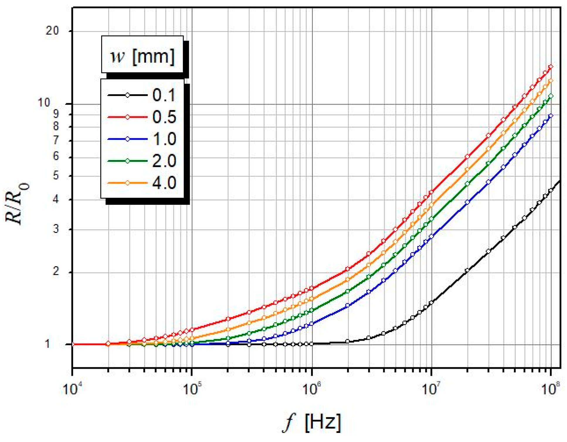
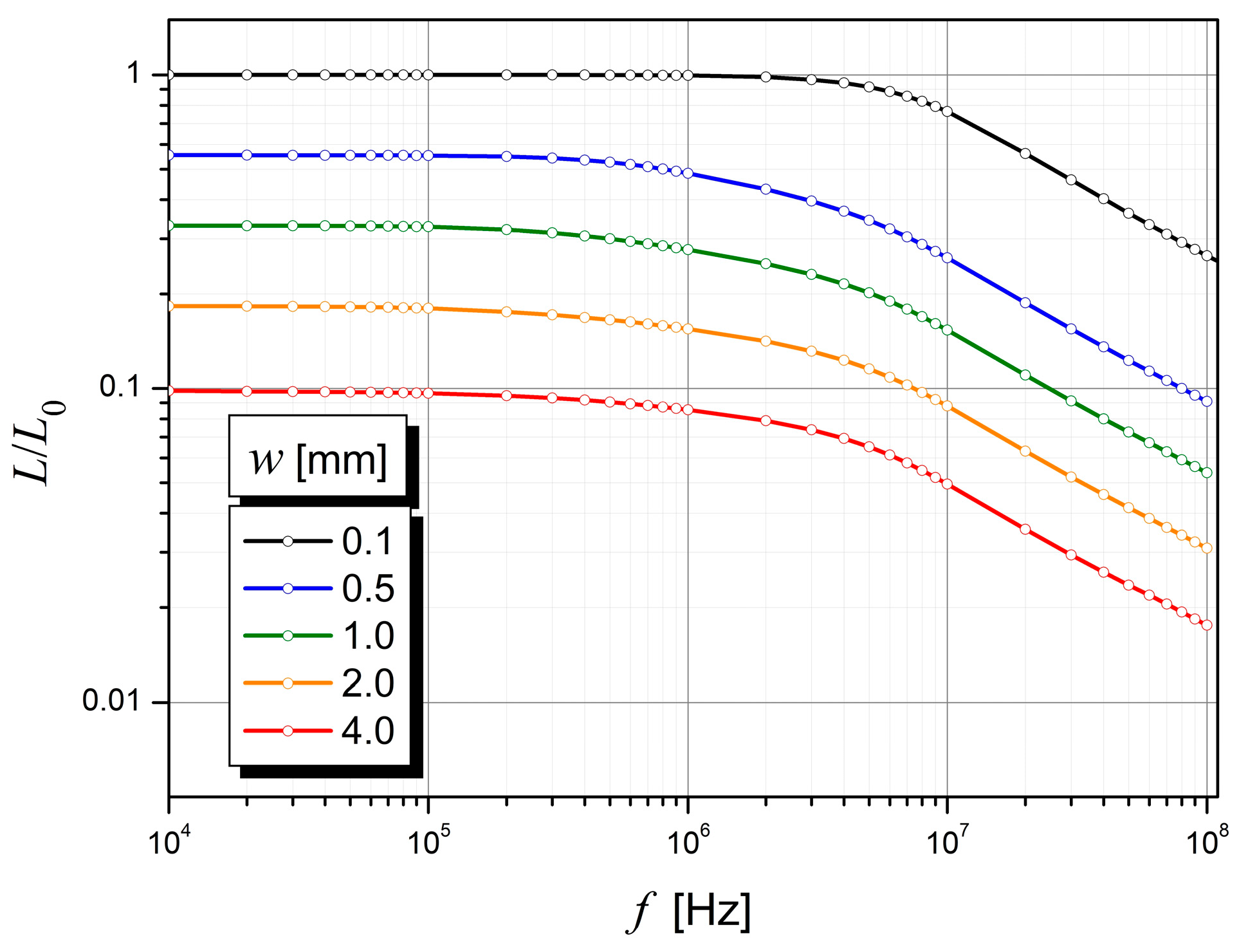
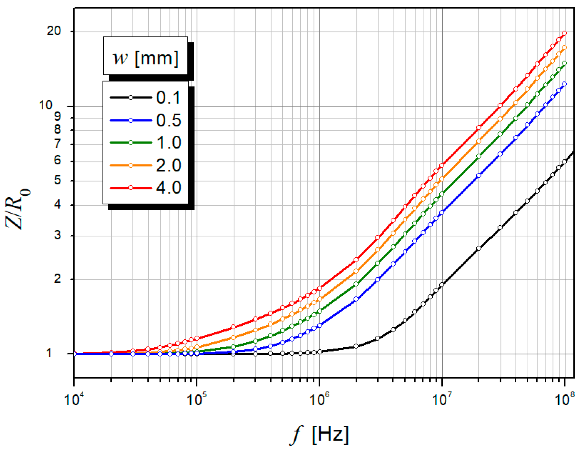
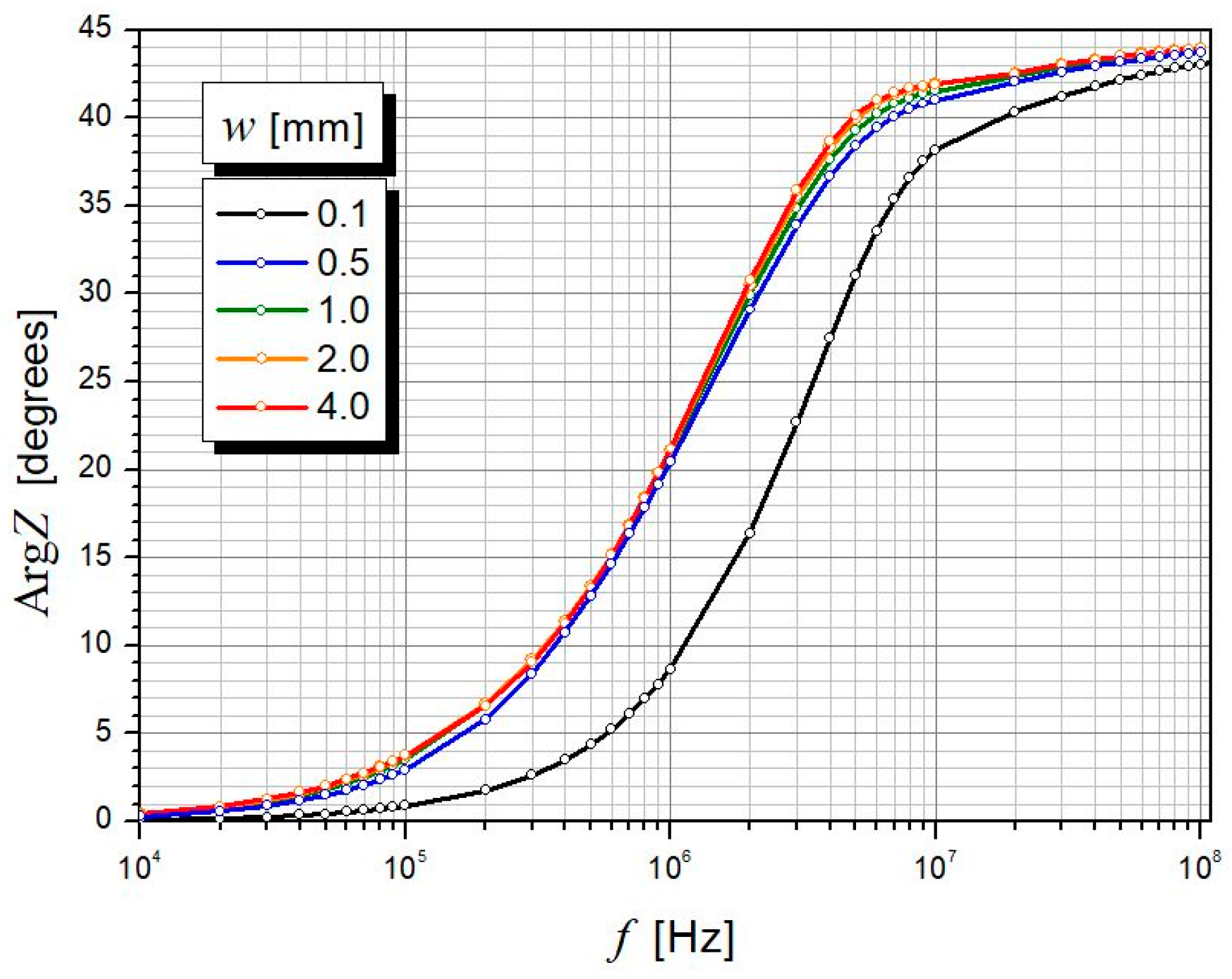
The graphs presented in Figure 5, Figure 6, Figure 7 and Figure 8 show the dependencies of the relative resistance, inductance and internal impedance per unit length on the frequency, calculated for a path with a thickness g = 0.1 mm and various widths w. The resistance and impedance modulus are related here to the resistance R0 that is characterized by the path with the same parameters and unit length carrying direct current ( R 0 = 1 / γ S c ), and the inductance is related to the inductance L0 of a wire with a circular cross-section and unit length with a low-frequency current (i.e., in the limit f → 0,  L 0 = μ / 8 π ). For comparison, graphs of these relationships are also shown for a circular wire with a diameter of 0.1 mm (black lines).
These relationships show that for paths with such parameters at frequencies lower than 10 kHz, the skin effect does not play a significant role. As the frequency increases above this value, the resistance increases rapidly and the internal inductance decreases, but its effective contribution to the impedance increases, which is reflected in the increase in the phase shift angle between the current and voltage (see Figure 8). It is worth noting that this angle depends very little on the width of the path, if it is at least several times larger than the thickness.
For frequencies above 10 MHz, the relationship between resistance and internal impedance on a double-logarithmic scale becomes almost linear, and the slope of these graphs for paths of different widths is very similar. It means that these relationships can be well approximated in this range by a power function with a similar exponent. The statistical analysis shows that it is approximately 0.65 ± 0.5, both for resistance and impedance.
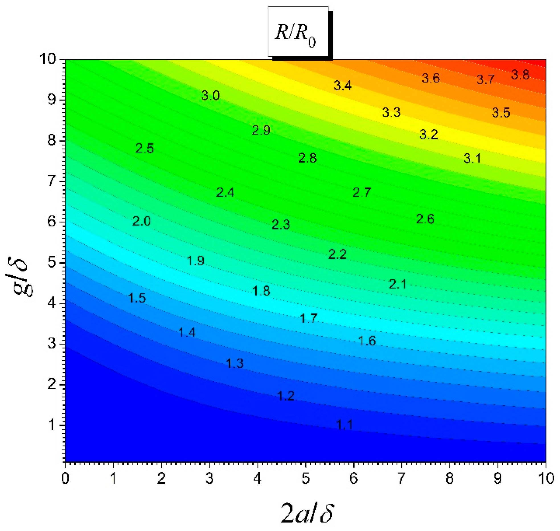
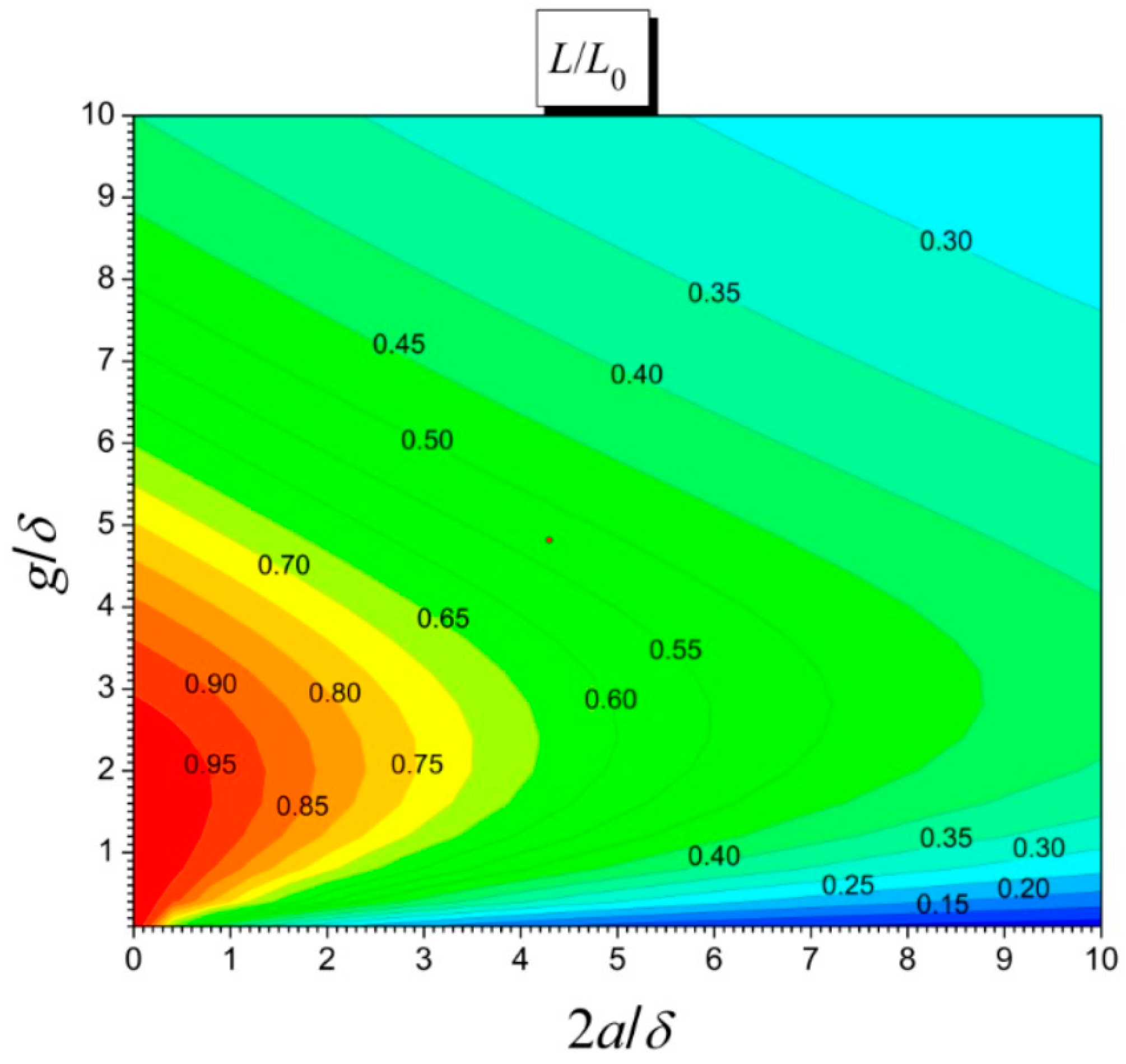
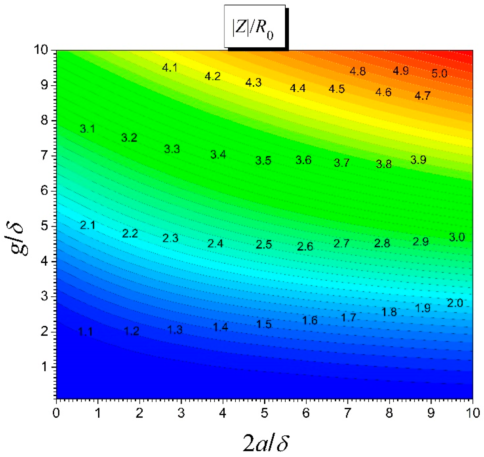
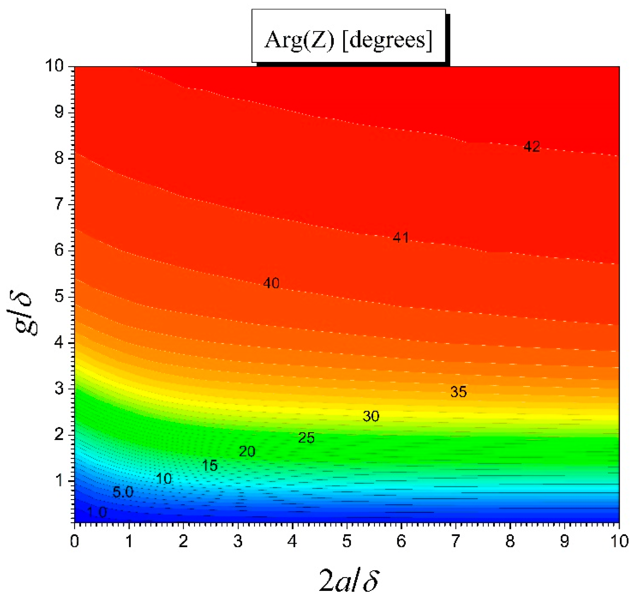
The results presented above are exemplary ones because they concern paths with the parameters of an arbitrarily selected material (silver) and arbitrarily set thicknesses and widths. In order to present results of a more universal nature, the graphs presented in Figure 9, Figure 10, Figure 11 and Figure 12 were prepared. They show the relationships between the resistance, internal inductance, modulus and argument of the internal impedance depending on the geometric dimensions of the path, related to the parameter, taking into account the total frequency and the equivalent field penetration depth which is the material parameter of the path.
δ = 2 ω γ μ
These graphs, combined with Formula (23), allow us to determine the impedance for a electroconductive path with an oval cross-section in a fairly wide range of current frequencies and geometric and material parameters.

5. Conclusions

The main goal of the work was to adapt and test the effectiveness of the fundamental solutions method for calculating the electromagnetic field distribution in the surroundings and inside of thin electroconductive paths with sinusoidally alternating current in a wide frequency range. The difficulties that arise in these types of issues are related, on the one hand, to the specific geometry of the thin path (its thickness is many times smaller than the other dimensions), and on the other, to the need to take into account skin, proximity and wave effects in the case of high-frequency currents. The strong skin effect means that it is not always possible to ignore changes in the electromagnetic and flow fields in the direction perpendicular to the surface of the conductive layer, despite its very small thickness. Moreover, even at lower frequencies, current displacement is observed from the center of the path to its side edges. Taking into account these effects requires appropriate discretization of the system areas and their edges, taking into account their high curvature near the side edges and the variability of the field function in all directions.
The tests and numerical simulations conducted allow us to formulate the following conclusions:
  • The correctness and effectiveness of the fundamental solutions method for the analysis of harmonics of electromagnetic fields in systems containing thin conductive layers were fully confirmed.
  • The created numerical program allows us to determine all important parameters of the transmission line determining its conductive properties, such as resistance, inductance and impedance in a wide frequency range.
  • In the high frequency range (above 10 MHz), the dependence of resistance and impedance on frequency on a double-logarithmic scale is linear, and the slope of these graphs does not depend (to a noticeable extent) on the path width. It means that in this range, the dependence of resistance and impedance on frequency can be well approximated by a power function with a constant exponent.
  • For paths whose width is at least several times greater than their thickness, the dependence of the shift angle between current and voltage on frequency depends very little on the path width.

Author Contributions

Conceptualization, S.P., J.P., E.K. and D.S.; methodology, S.P., J.P. and E.K.; software, S.P. and J.P. validation, S.P., J.P. and E.K.; formal analysis, S.P., J.P. and E.K.; investigation, S.P., J.P. and E.K.; data curation, S.P., J.P., E.K. and D.S.; writing—original draft preparation, S.P., J.P., E.K. and D.S.; writing—review and editing, S.P., J.P. and E.K.; visualization, S.P., J.P. and E.K.; supervision, S.P., J.P. and E.K. All authors have read and agreed to the published version of the manuscript.

Funding

This research received no external funding.

Institutional Review Board Statement

Not applicable.

Informed Consent Statement

Not applicable.

Data Availability Statement

The data presented in this study are available on request from the corresponding author.

Conflicts of Interest

The authors declare no conflict of interest.

References

  1. Valero, E.; Adán, A.; Cerrada, C. Evolution of RFID Applications in Construction: A Literature Review. Sensors 2015, 15, 15988–16008. [Google Scholar] [CrossRef]
  2. Lee, T.Y.; Ahmad, F.; Rahman, M.A.A.; Awang, M. RFID-cloud construction equipment management system framework: Current issues and user needs. Mater. Today Proc. 2022. [Google Scholar] [CrossRef]
  3. Korzeniewska, E.; Szczęsny, A.; Lipiński, P.; Dróżdż, T.; Kiełbasa, P.; Miernik, A. Prototype of a Textronic Sensor Created with a Physical Vacuum Deposition Process for Staphylococcus aureus Detection. Sensors 2021, 21, 183. [Google Scholar] [CrossRef]
  4. Communications of Huawei Research. September 2022. Available online: www-file.huawei.com/-/media/corp2020/pdf/publications/huawei-research/2022/huawei-research-issue2-en.pdf (accessed on 18 August 2023).
  5. Pandiyan, A.; Veeramuthu, L.; Yan, Z.-L.; Lin, Y.-C.; Tsai, C.-H.; Chang, S.-T.; Chiang, W.-H.; Xu, S.; Zhou, T.; Kuo, C.-C. A comprehensive review on perovskite and its functional composites in smart textiles: Progress, challenges, opportunities, and future directions. Prog. Mater. Sci. 2023, 140, 101206. [Google Scholar] [CrossRef]
  6. Goyal, K.; Borkholder, D.A.; Day, S.W. Dependence of Skin-Electrode Contact Impedance on Material and Skin Hydration. Sensors 2022, 22, 8510. [Google Scholar] [CrossRef]
  7. Available online: www.huawei.com/en/huaweitech/future-technologies/6g-isac-ow (accessed on 18 August 2023).
  8. Pawłowski, S.; Plewako, J.; Korzeniewska, E. Analysis of flow field distribution in a thin conductive layer with an elliptical defect. Prze. Elektrotech. 2020, 96, 234–237. [Google Scholar] [CrossRef]
  9. Miśkiewicz, P.; Frydrych, I.; Cichocka, A. Application of Physical Vapor Deposition in Textile Industry. Autex Res. J. 2022, 22, 42–54. [Google Scholar] [CrossRef]
  10. Hong, H.C.; Ryu, J.I.; Lee, H.C. Recent Understanding in the Chemical Vapor Deposition of Multilayer Graphene: Controlling Uniformity, Thickness, and Stacking Configuration. Nanomaterials 2023, 13, 2217. [Google Scholar] [CrossRef]
  11. Białostocka, A.M. The electrochemical copper structure forming in the presence of the magnetic field. Prze. Elektrotech. 2013, 89, 254–256. [Google Scholar]
  12. Yin, Y. Advances and perspectives of spin coating techniques. Appl. Comput. Eng. 2023, 7, 291–301. [Google Scholar] [CrossRef]
  13. Wang, Z.; Bokov, D.; Turki Jalil, A.; Chupradit, S.; Suksatan, W.; Javed Ansari, M.; Shewael, I.H.; Valiev, G.H.; Kianfar, E. Nanomaterial by Sol-Gel Method: Synthesis and Application. Adv. Mater. Sci. Eng. 2021, 2021, 5102014. [Google Scholar] [CrossRef]
  14. Skolik, M.; Karasiński, P. Single- and double-layer antireflective structures fabricated via sol-gel method for applications in silicon solar cells. Prze. Elektrotech. 2017, 93, 8. [Google Scholar] [CrossRef]
  15. Karasinski, P. Dielectric layers fabricated via sol-gel method and dip-coating technique for applications in optoelectronics. Prze. Elektrotech. 2019, 95. [Google Scholar] [CrossRef]
  16. Kisała, J. Influence of an additional magnetic field during magnetron sputtering on the GMR effect in thin-film structures. Prze. Elektrotech. 2022, 98, 192–195. [Google Scholar] [CrossRef]
  17. Jankowski-Mihułowicz, P.; Tomaszewski, G.; Węglarski, M. Flexible antenna design for semi-passive HF RFID transponder in ink-jet technology. Prze. Elektrotech. 2015, 91, 1–5. [Google Scholar] [CrossRef]
  18. Chung, S.; Cho, K.; Lee, T. Recent Progress in Inkjet-Printed Thin-Film Transistors. Adv. Sci. 2019, 6, 1801445. [Google Scholar] [CrossRef]
  19. Goh, G.L.; Tay, M.F.; Lee, J.M.; Ho, J.S.; Sim, L.N.; Yeong, W.Y.; Chong, T.H. Potential of Printed Electrodes for Electrochemical Impedance Spectroscopy (EIS): Toward Membrane Fouling Detection. Adv. Electron. Mater. 2021, 7, 23. [Google Scholar] [CrossRef]
  20. Fastier-Wooller, J.W.; Dau, V.T.; Dinh, T.; Tran, C.-D.; Dao, D.V. Pressure and temperature sensitive e-skin for in situ robotic applications. Mater. Des. 2021, 208, 109886. [Google Scholar] [CrossRef]
  21. Lin, Z.; Huang, Y.; Duan, X. Van der Waals thin-film electronics. Nat. Electron. 2019, 2, 378–388. [Google Scholar] [CrossRef]
  22. Tomczyk, M.; Kubik, P.; Waliszewski, W. Optimization of the Ablative Laser Cutting of Shadow Mask for Organic FET Electrode Fabrication. Electronics 2020, 9, 2184. [Google Scholar] [CrossRef]
  23. Korzeniewska, E.; Sekulska-Nalewajko, J.; Gocławski, J.; Rosik, R.; Szczęsny, A.; Starowicz, Z. Surface Morphology Analysis of Metallic Structures Formed on Flexible Textile Composite Substrates. Sensors 2020, 20, 2128. [Google Scholar] [CrossRef]
  24. Kłosowski, G.; Rymarczyk, T.; Niderla, K.; Kulisz, M.; Skowron, Ł.; Soleimani, M. Using an LSTM network to monitor industrial reactors using electrical capacitance and impedance tomography—A hybrid approach. Eksploat. I Niezawodn. Maint. Reliab. 2023, 25, 11. [Google Scholar] [CrossRef]
  25. Młot, A.; Korkosz, M.; Grodzki, P.; Łukaniszyn, M. Analysis of proximity effect and skin effect on copper loss in armature. Prze. Elektrotech. 2013, 89, 44–48. [Google Scholar] [CrossRef]
  26. Asada, T.; Baba, Y.; Nagaoka, N.; Ametani, A.; Mahseredjian, J.; Yamamoto, K. A Study on Basic Characteristics of the Proximity Effect on Conductors. IEEE Trans. Power Deliv. 2017, 32, 1790–1799. [Google Scholar] [CrossRef]
  27. Kupradze, V.D.; Aleksidze, M.A. Approximate method of solving certain boundary-value problems. Soobsc. Akad. Nauk Gruzin. SSR 1963, 30, 529–536. (In Russian) [Google Scholar]
  28. Mączka, M.; Hałdaś, G. Three dimensional simulator of the single electron transistor based on ISIS structure. Phys. E Low-Dimens. Syst. Nanostructures 2012, 44, 1202–1208. [Google Scholar] [CrossRef]
  29. Pawłowski, S.; Plewako, J.; Grodzki, P. Efficiency comparison of the fundamental solutions iterative method and finite element method in the analysis of electrostatic problems. Prze. Elektrotech. 2017, 93, 12. [Google Scholar] [CrossRef]
  30. Jackson, J.D. Classical Electrodynamics; OCLC 925677836; John Wiley & Sons: New York, NY, USA, 1999; ISBN 978-0-471-30932-1. [Google Scholar]
  31. Gradshteyn, I.S.; Ryzhik, I.M. Table of Integrals, Series, and Products; Elsevier: Amsterdam, The Netherlands, 2007; ISBN 13-978-0-12-373637-6. [Google Scholar]
  32. Mączka, M. Effective Simulations of Electronic Transport in 2D Structures Based on Semiconductor Superlattice Infinite Model. Electronics 2020, 9, 1845. [Google Scholar] [CrossRef]
  33. Mączka, M.; Hałdaś, G. Calculations of transport parameters in semiconductor superlattices based on the Green’s functions method in different Hamiltonian representations. Bull. Pol. Acad. Sci. Tech. Sci. 2019, 67, 3. [Google Scholar] [CrossRef]
  34. Pawłowski, S. Applicability assessment for simplified formulas to compute surface impedance at screened surfaces. Prze. Elektrotech. 2015, 1, 184–186. [Google Scholar] [CrossRef]
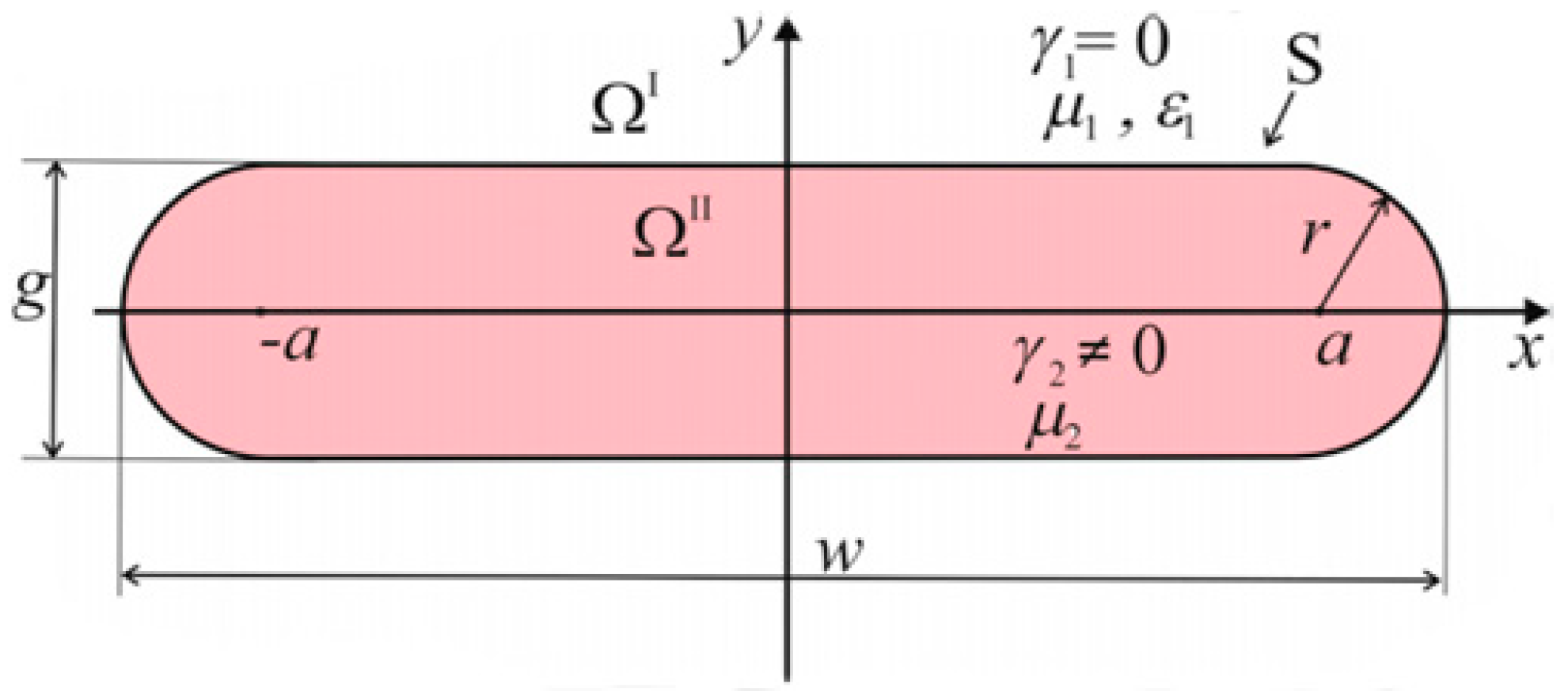
Figure 1. Cross-section of the conductive path (analyzed model). ΩI, ΩII—non-conductive and conductive areas; μ1, ε1, γ1—material parameters in the non-conductive area; μ2, γ2—material parameters in the conductive area; S—cross-section of the conductive path; r—radius of curvature of the conductive path; g—thickness of the conductive path; w—width of the conductive path.
Electronics 12 04834 g001
Figure 2. Illustration of the fundamental solution method—distribution of fictitious sources and nodes in the analyzed conductive path model.
Electronics 12 04834 g002
Figure 3. Example results of calculations of the electric field strength and magnetic induction components in the analyzed model. Conductive silver path with dimensions 0.2 × 1.0 mm, I = 1 A, f = 1 MHz.
Electronics 12 04834 g003aElectronics 12 04834 g003b
Figure 4. Example results of calculations of the current density distribution in the analyzed model at different frequencies. Conductive silver path with dimensions 0.2 × 1.0 mm, I = 1 A.
Electronics 12 04834 g004
Figure 5. Resistance of oval paths with conductivity γ = 63 × 106 S/m (Ag), thickness g = 0.1 mm and different widths w as a function of frequency.
Electronics 12 04834 g005
Figure 6. Internal inductance of oval paths with conductivity γ = 63 × 106 S/m (Ag), thickness g = 0.1 mm and different widths w as a function of frequency.
Electronics 12 04834 g006
Figure 7. Internal impedance modulus of oval paths with conductivity γ = 63 × 106 S/m (Ag), thickness g = 0.1 mm and different widths w as a function of frequency.
Electronics 12 04834 g007
Figure 8. Internal impedance of oval paths with conductivity γ = 63 × 106 S/m (Ag), thickness g = 0.1 mm and different widths w as a function of frequency.
Electronics 12 04834 g008
Figure 9. Relative resistance of the path per unit length depending on its thickness g and the length of the flat part 2a (see Figure 1) related to the equivalent field penetration depth δ.
Electronics 12 04834 g009
Figure 10. Relative inductance of the path per unit length depending on its thickness g and the length of the flat part 2a (see Figure 1) related to the equivalent field penetration depth δ.
Electronics 12 04834 g010
Figure 11. Relative impedance of the path per unit length depending on its thickness g and the length of the flat part 2a (see Figure 1) related to the equivalent field penetration depth δ.
Electronics 12 04834 g011
Figure 12. Impedance argument of the path depending on its thickness g and the length of the flat part 2a (see Figure 1) related to the equivalent field penetration depth δ.
Electronics 12 04834 g012
Disclaimer/Publisher’s Note: The statements, opinions and data contained in all publications are solely those of the individual author(s) and contributor(s) and not of MDPI and/or the editor(s). MDPI and/or the editor(s) disclaim responsibility for any injury to people or property resulting from any ideas, methods, instructions or products referred to in the content.