Abstract
With the emergence of 5G and satellite communication applications, where millimeter-wave (mm-wave) active phased arrays play an important role, the demand for a highly integrated and cost-effective method to achieve mm-wave antennas is an inevitable trend. Antenna-in-package (AiP) design is therefore becoming a hotspot. This paper presents the design procedure for a broadband silicon-based stacked patch antenna in Ka-band, which realizes a practical AiP structure for phased-array module integration requirements. A stacked-patch antenna on a high-resistivity silicon (HRSi) substrate is demonstrated to effectively extend the bandwidth with the guidance of characteristic mode analysis (CMA).The proposed antenna element and its 2 × 2 array were designed and fabricated using silicon bulk micromachining and wafer-level bonding technology. The measured results from the fabricated antenna prototypes showed that (1) the antenna element had an impedance bandwidth of 13.8% from 26.2 to 30.1 GHz, and the peak gain was 6.1 dBi at 28.9 GHz; (2) the 2 × 2 array realized an impedance bandwidth of 11.4% from 27.2 to 30.5 GHz, and the peak gain was 9.3 dBi at 28.5 GHz.
1. Introduction
In recent years, there has been an increasing demand for high data rates and wide transmission bandwidth in the mobile communication field, such as for 5G communication and satellite communication, which leads to higher frequencies above 20 GHz. In the Ka-band, active phased array systems for satellite communication with large capacities and compact structures play an important role in mobile communication. In higher frequency bands, the interconnection loss between a traditional passive antenna and the active transceiver module becomes higher, and the efficiency is low, which reduces the performance of the traditional active phased array. Improving the integration of the antenna and RF system has become a current development trend in millimeter wave active phased array systems. A high frequency naturally contributes to a highly integrated design. By utilizing the small size of millimeter-wave devices, it is possible to assemble multiple functional blocks and antennas in a package using a packaging process, which is called system-in-package (SiP) technologies. Antenna design has shifted from the conventional discrete antenna approach to an antenna-in-package (AiP) solution [1], and high-performance AiP and arrays have become a research hotspot in the field of antennas [2,3,4,5,6,7,8,9]. In the specific designs, a microstrip antenna is widely used in the design of AiP because of its planar structure and easy integration with active circuits. In addition, a variety of innovative substrate technologies have been explored for mm-wave antenna design and system integration to date, including organic high-density interconnect (HDI) substrates, low-temperature co-fired ceramic (LTCC) substrates, molding-compound-based wafer-level substrates, and silicon substrates. LTCC has been widely used in phased array scanning antenna arrays [2,3,4] in recent years, due to its high machining accuracy, low loss, and design flexibility. However, the high cost of this process limits its market to mm-wave applications. Therefore, manufacturers have studied low-cost HDI processes suitable for mass production. IBM has developed various AiP arrays operating in the Ka-band and W-band for mm-wave 5G communication systems based on the HDI process [5,6,7]. Molding compounds are materials used in the fan-out wafer-level packaging (FOWLP) process, which is known as eWLB. Several works of AiP design based on this process have been reported so far [8,9].
Silicon substrate, as one of the most important materials for the integrated circuit industry, can be used to manufacture mm-wave antennas for a highly integrated purpose. At present, the mainstream silicon processing technologies include CMOS, SiGe, and the silicon-based 3D integration process based on bulk silicon micromachining and chip micro-assembly processes [10]. The CMOS process and SiGe process utilize the advantages of semiconductor processes and are mainly used for manufacturing antenna-on-chip (AoC) and on-chip radar systems above 60 GHz. However, the silicon substrate with low resistivity results in a poor radiation efficiency [11]. The silicon-based 3D integration process is more flexible, enabling integration solutions such as heterogeneous integration and high-precision heterogeneous integration in silicon technology. The bulk silicon micromachining process is used to etch the cavity on the silicon substrate for placing the chip and for the cover plate, to create through-silicon-vias (TSVs), and generate metal graphics. Through th micro-assembly process, a mm-wave chip is sintered into the cavity through gold wire bonding. Then, low-temperature wafer-level bonding is performed, and finally, three-dimensional integrated microsystems [12,13] and T/R modules [14,15] are obtained through slicing and segmentation. Therefore, a microstrip antenna manufactured through standard silicon process can be easily assembled with other active chips, providing a cost-effective solution for mm-wave AiP design.
In practical application scenarios, typical requirements for antennas include sufficient bandwidth, stable antenna gain within the bandwidth, and radiation patterns, to achieve the optimal beam scanning capability for phased arrays. However, the high permittivity of substrates, which can result in a high quality factor (Q value) for antennas and trigger surface waves, hinders silicon-based antennas from achieving high performance. Aiming at the above problems, Ioannis et al. [16] tried to reduce the equivalent dielectric constant of the substrate by removing a portion of the silicon substrate below the antenna, resulting in increases in antenna bandwidth and efficiency of 64% and 28%, respectively. Gauthier et al. [17] processed closely spaced holes on a high dielectric-constant substrate to synthesize a localized low dielectric-constant environment, thereby increasing the antenna bandwidth. However, these methods are somewhat complicated during manufacturing and not suitable for further integration and mass production.
In this paper, a Ka-band silicon-based broadband stacked patch antenna based on bulk silicon micromachining technology is presented. The proposed antenna uses three layers of silicon, with each layer of 250 m stacked using high-precision wafer-level bonding technology. A high-resistivity silicon (HRSi) substrate is used to improve the antenna’s gain performance. By enlarging the aspect ratio of the upper patch and adding a slotted patch as a double-tuned resonator, the bandwidth of the silicon-based antenna is effectively enhanced. The design of the antenna was guided by the theory of characteristic mode, revealing the principle of performance enhancement. Consequently, a 2 × 2 subarray was presented to validate the antenna performance. The prototype unit has a measured impedance bandwidth (S11 ≤ −10 dB) of 13.8% from 26.2 GHz to 30.1 GHz. The peak boresight gain reaches 6.1 dBi in the operating frequency band, and the overall size of the unit is 5 mm × 5 mm × 0.78 mm (0.470 × 0.470 × 0.070 at 28 GHz). The measured impedance bandwidth of the 2 × 2 subarray is 11.4% from 27.2 GHz to 30.5 GHz, with a peak boresight gain of 9.3 dBi in the operating frequency band and a size of 9 mm × 9 mm × 0.78 mm (0.840 × 0.840 × 0.070). The antenna structure adopts an HRSi substrate, without the need for isomerism with other substrates or cavity-etching processes, which not only has certain advantages in mechanical reliability and consistency, but also makes it suitable for mass production. Furthermore, the subarray can be extended to an N × N mm-wave active phased array.
2. Antenna Design Approach
2.1. Silicon-Based Antenna Design with Enhanced Bandwidth
Using a high-permittivity substrate for microstrip antennas generally leads to penalties in performance [18], which is seen to be contrary to MMICs. For instance, the bandwidth of a microstrip patch for r = 12.8 is less than 5% when d/0 < 0.04, and the surface wave power accounts for nearly half of the total input power when d/0 > 0.045 [19].
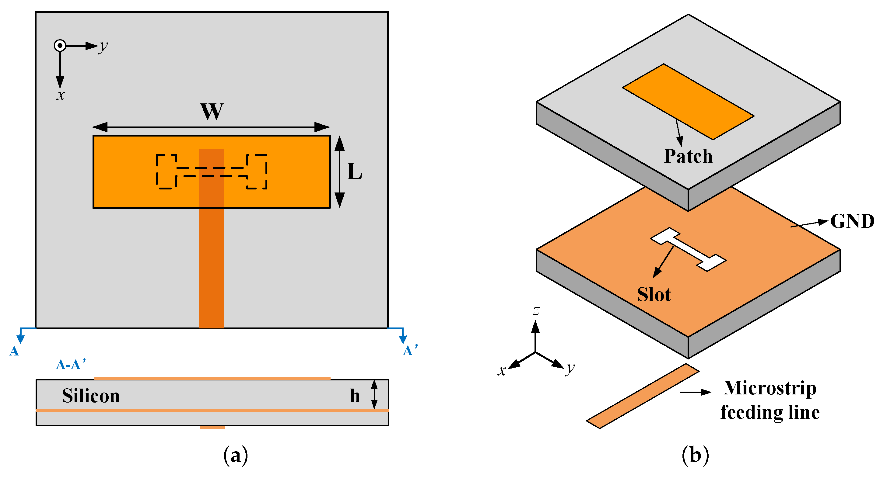
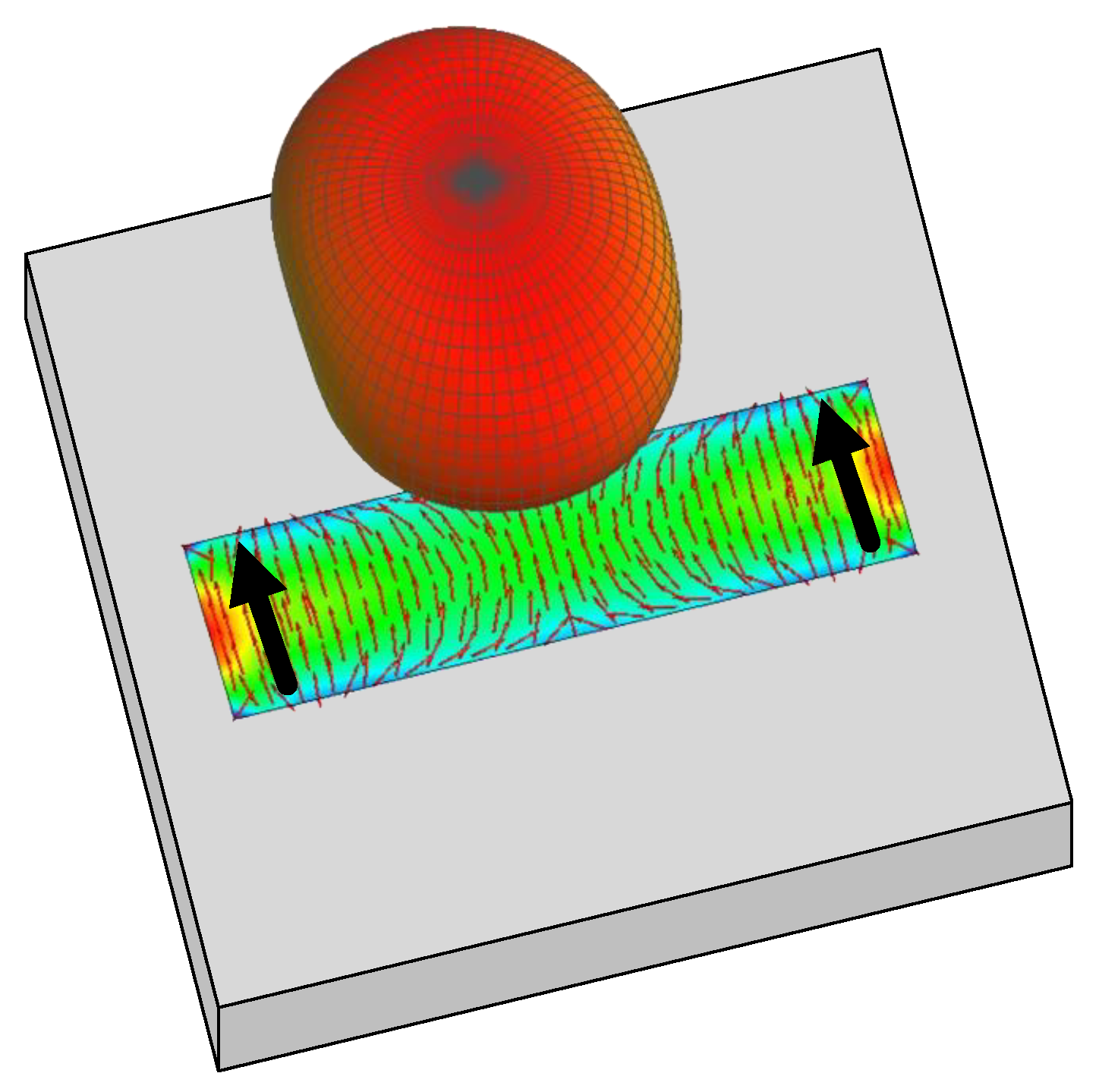
With high-permittivity silicon (r = 11.9) showing fundamental issues and design challenges for microstrip antennas, it is necessary to enlarge the area of the radiation element or thicken the substrate for bandwidth enhancement [20]. Silicon-based rectangular patch antennas in four different dimensions are discussed with the aid of CMA, which describes the resonance behavior of each mode on the electromagnetic structure and the radiation behavior in the far-field zone [21]. Figure 1 shows the model used in the discussion. The rectangular patch is located on silicon with thickness h and is fed by the microstrip line through the H-shaped aperture coupling on the ground. Specifically, case 1 has the same thickness (h = 0.5 m) as case 2 and the same patch width (W = 5 mm) as case 3. The thickness discussed here is based on each silicon wafer being 250 m thick.
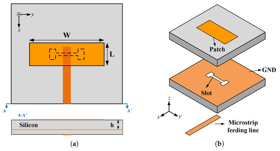
Figure 1.
Configuration of the microstrip patch antenna. (a) Top and side view; (b) exploded view.
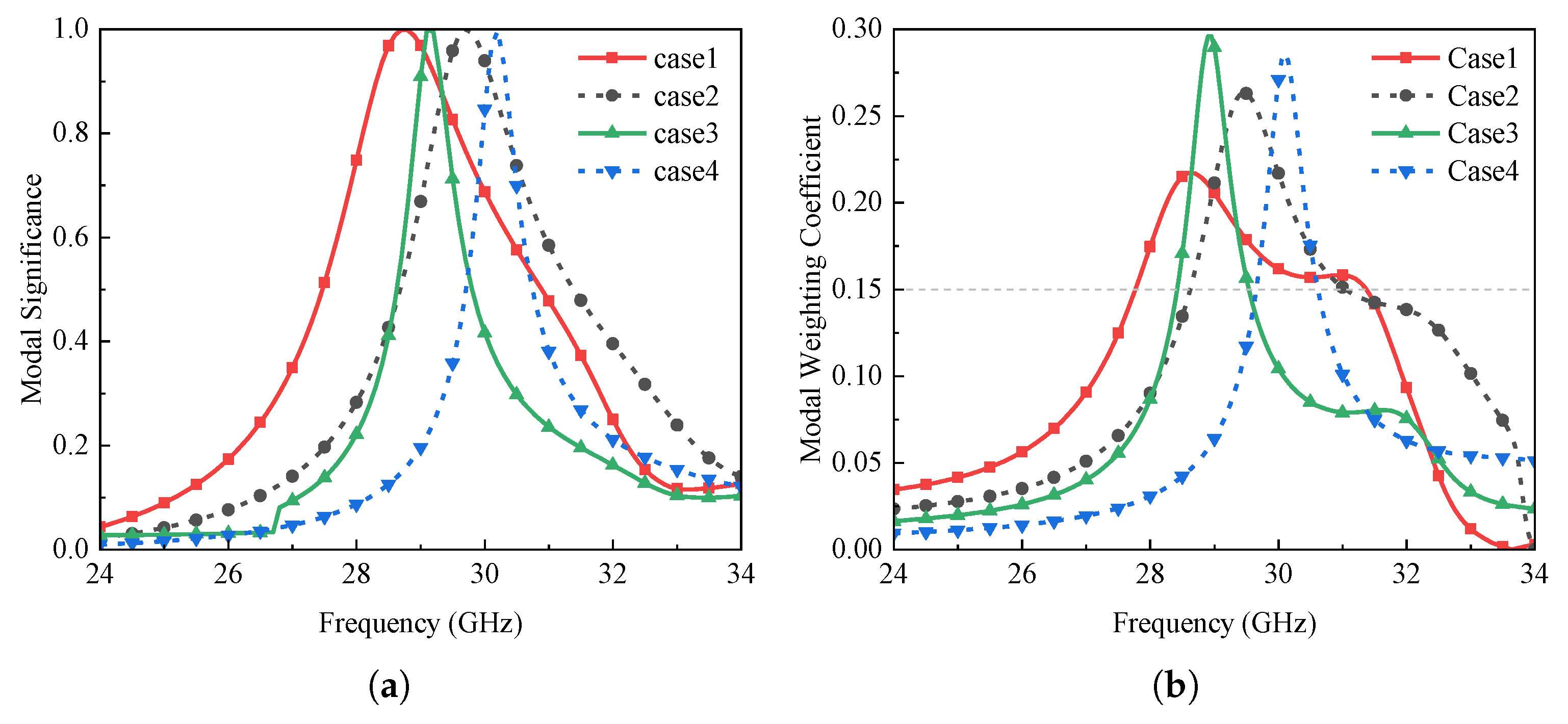
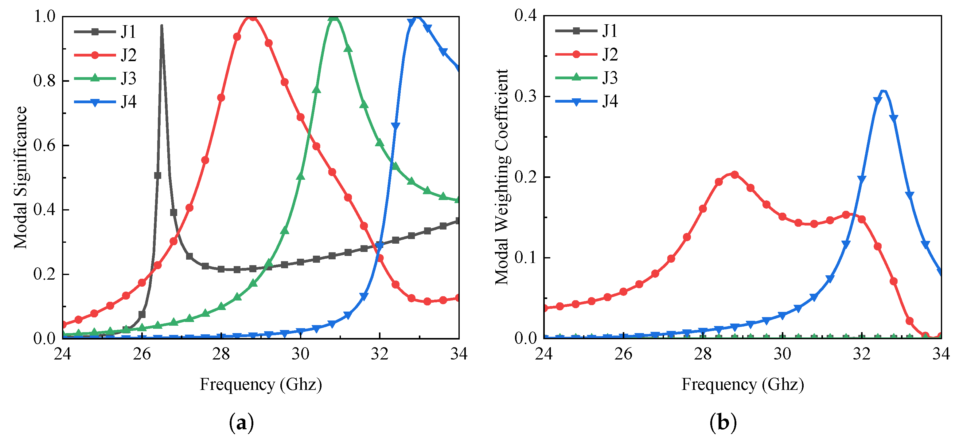
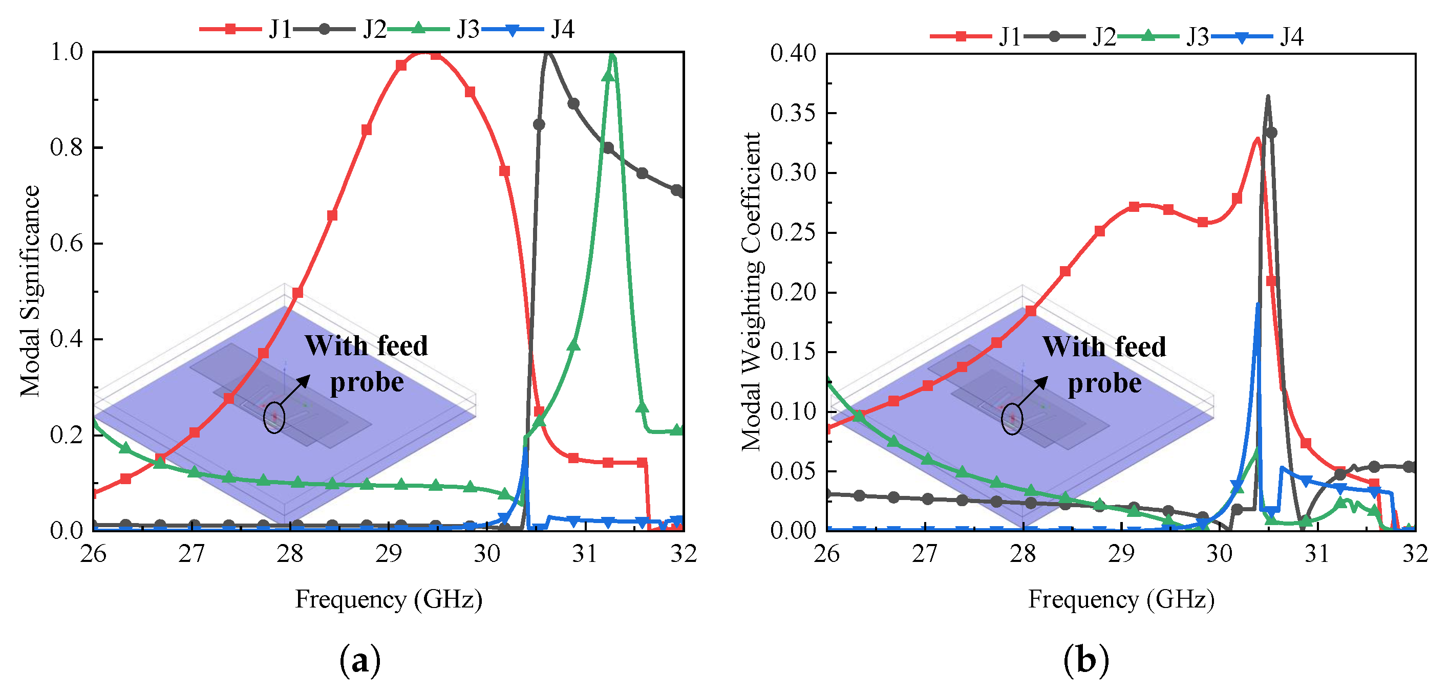
Figure 2 shows the MS and MWC curves of the dominant mode in the four cases. The characteristic currents and far-field radiation of the dominant mode are shown in Figure 3. Note that the MWC curve for case 1 has two peaks, whose values are both larger than 0.15. It is supposed that other modes have an impact on the result. Figure 4 displays the MS and MWC results for case 1, from which we can see there are four resonant modes in the range and two of them are excited (J2 and J4). The characteristic currents and fields are shown in Figure 5. According to the current distributions, it can be determined that J2 refers to the TM10 mode and J4 refers to the TM10 mode. Therefore, the second peak in J2’s MWC curve resulted from the onset of J4.
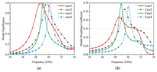
Figure 2.
(a) MS and (b) MWC of the dominant mode. Case 1: W = 5 mm, L = 1.08 mm, h = 0.5 mm; Case 2: W = 2 mm, L = 1.11 mm, h = 0.5 mm; Case 3: W = 5 mm, L = 1.39 mm, h = 0.25 mm; Case 4: W = 3 mm, L = 1.39 mm, h = 0.25 mm.

Figure 3.
Characteristic currents and far-field radiation of the dominant mode.
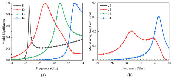
Figure 4.
(a) MS and (b) MWC of the antenna with the dimensions of case 1.
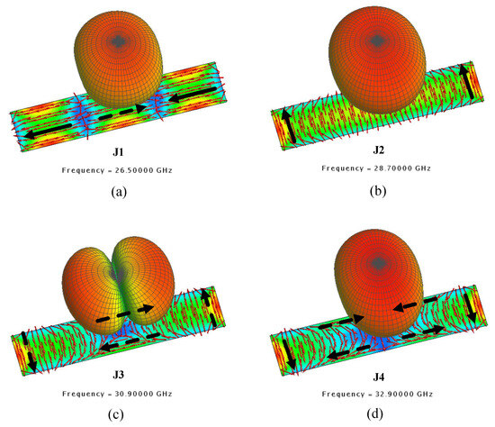
Figure 5.
Characteristic currents and characteristic fields of four modes. (a) J1; (b) J2; (c) J3; (d) J4.
The reflection coefficients of the antennas in the four cases (obtained using a full-wave simulation) are shown in Figure 6. It is seen that the best impedance matching in case 1 occurs in the middle of the two peaks in the MWC curve. Thanks to the joint effect of J2 and J4 on the input impedance, the antenna in case 1 has the widest bandwidth of 11.2%.
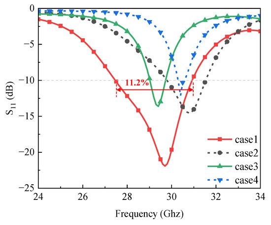
Figure 6.
Simulated S11 of antennas in the four cases.
With the large ratio-aspect patch (W/L = 4.6) and two silicon layers (h = 500 m), the bandwidth is effectively extended. However, the large patch width imposes a penalty on the array design, considering the spacing requirement (typically 0.50) between the antenna elements at millimeter-wave frequencies.
New microstrip configurations with a wider bandwidth have been exhaustively explored. In [22], a U-shaped slot was etched on a patch to generate an additional resonance. In [23], multiple stacked patches, with the upper patches acting as electromagnetically coupled parasitics, were designed for extending bandwidths. Based on the above works, the configuration of stacked patches with lower patch etched U-slots is proposed in this paper. The design approach is presented step by step using CMA, to reveal the radiation mechanism of the structure.
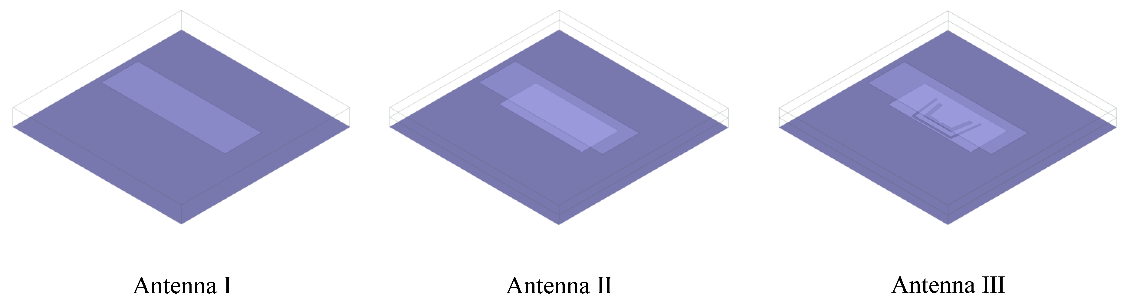
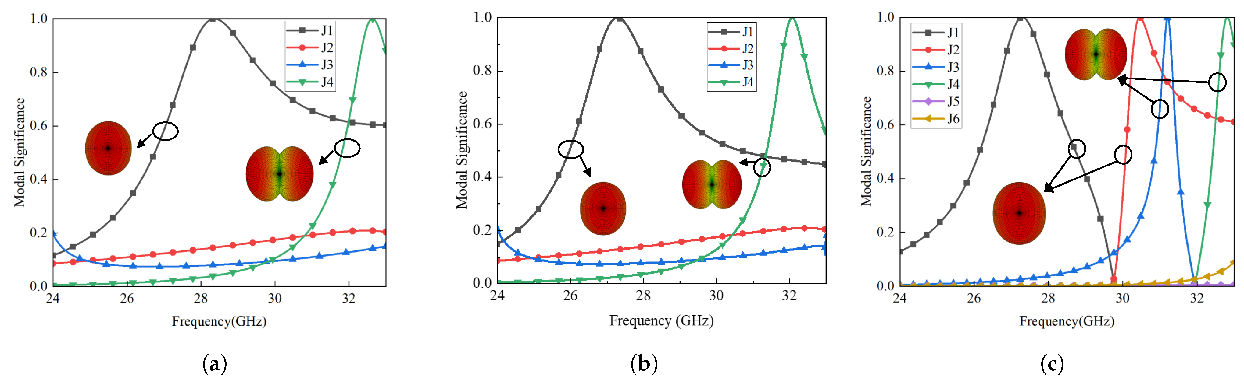
An evolution of the proposed antenna is shown in Figure 7. Antenna I is a single patch with W/L = 3.4 and h = 500 m, and Antenna II adds a lower patch and maintains the same profile. Antenna III etches double U-shaped slots on the lower patch. Figure 8 shows the MS curves and far-field patterns of antenna I to antenna III. The results were obtained without the feeding structure, since MS is independent of any sources. It is seen that the MS curve of Antenna I and Antenna III only had one resonant mode radiating unidirectionally, while the MS curve of Antenna III showed two desired modes in this frequency band.
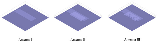
Figure 7.
Configurations of antennas I to III.
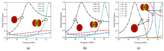
Figure 8.
MSs and corresponding radiation patterns of the three source-free antennas. (a) Antenna I; (b) Antenna II; (c) Antenna III.
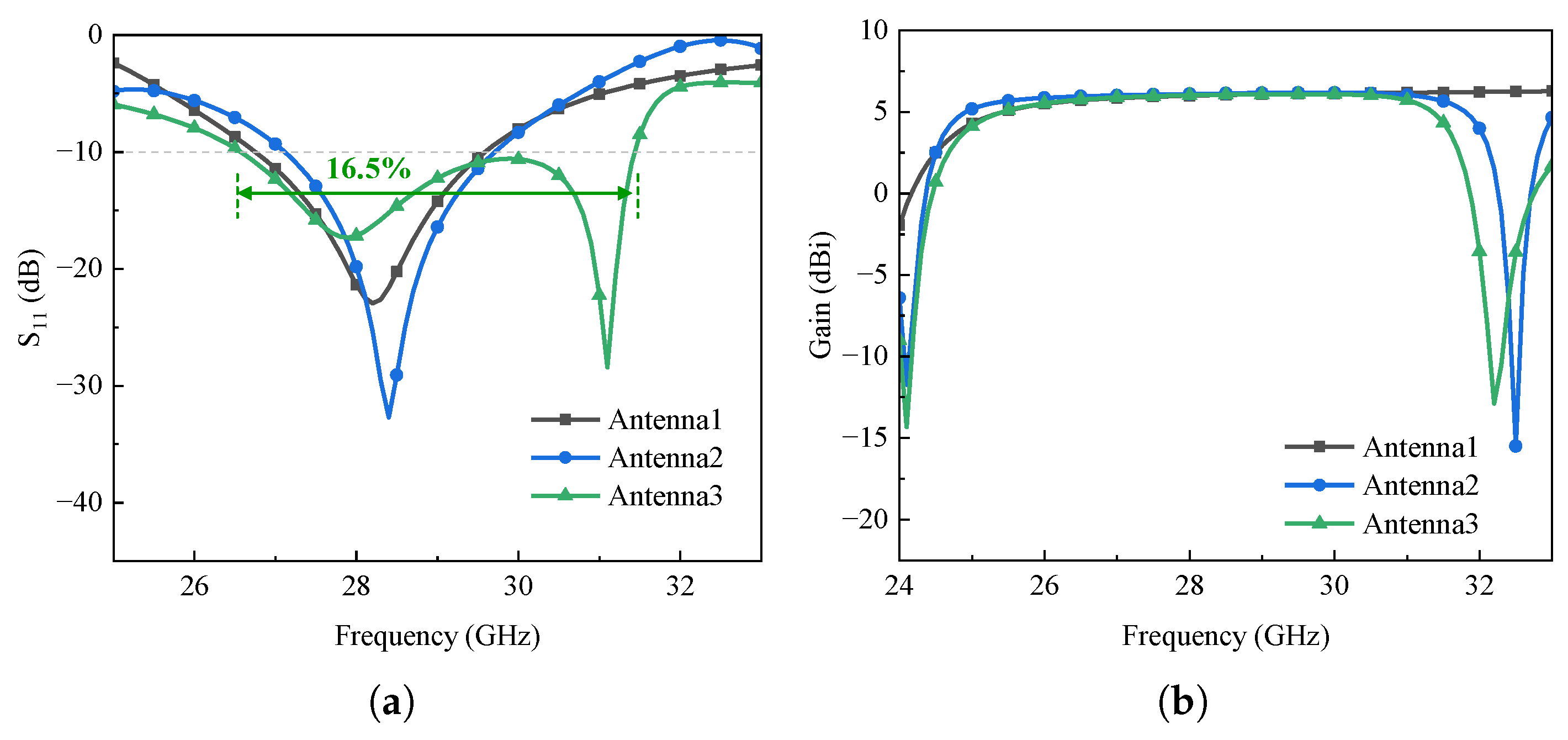
Figure 9a shows the MS of antenna III with a probe-feed structure. Compared with Figure 8c, the MS curves shifted to higher frequencies, due to the introduction of the feeding probe. From Figure 9b, we can see there are two modes excited (J1 and J2). Figure 10 shows the characteristic currents and far-field radiation pattern when J1 and J2’s MS = 1, respectively. Note that the characteristic currents near resonance for J1 and J2 show in-phase and anti-phase relationships, while both modes present the maximum radiation in boresight. In our opinion, the far-field radiation depended mainly on the top patch currents coupled by the bottom patch, which serves as a “double tuned” matching [24] resonator. The simulated results using full-wave simulation are shown in Figure 11. Compared with Antenna I and II, the S11 curve of Antenna III had a double-resonant response and realized a 10 dB impedance bandwidth of 16.5%. Within this bandwidth, a gain performance of more than 5.5 dBi in boresight was realized for the three antennas, due to the high resistivity of silicon. Note that the boresight gains of Antenna II and Antenna III both had nulls near 24 GHz and 32 GHz beyond the band. This was caused by the opposite current distribution in the y direction.
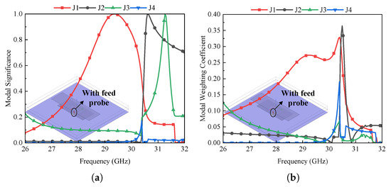
Figure 9.
(a) MS and (b) MWC of Antenna III with feed.
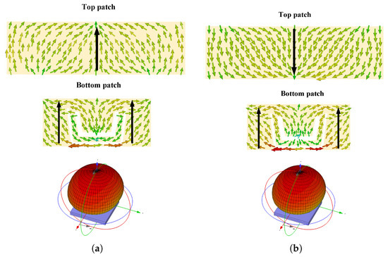
Figure 10.
Characteristic currents and far fields of the stacked patch. (a) J1 at 29.3 GHz; (b) J2 at 30.7 GHz.
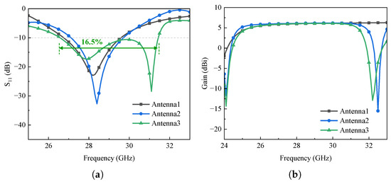
Figure 11.
Full-wave simulated results for Antenna I to III. (a) S11; (b) boresight gain.
2.2. Structure of the Proposed Antenna Unit
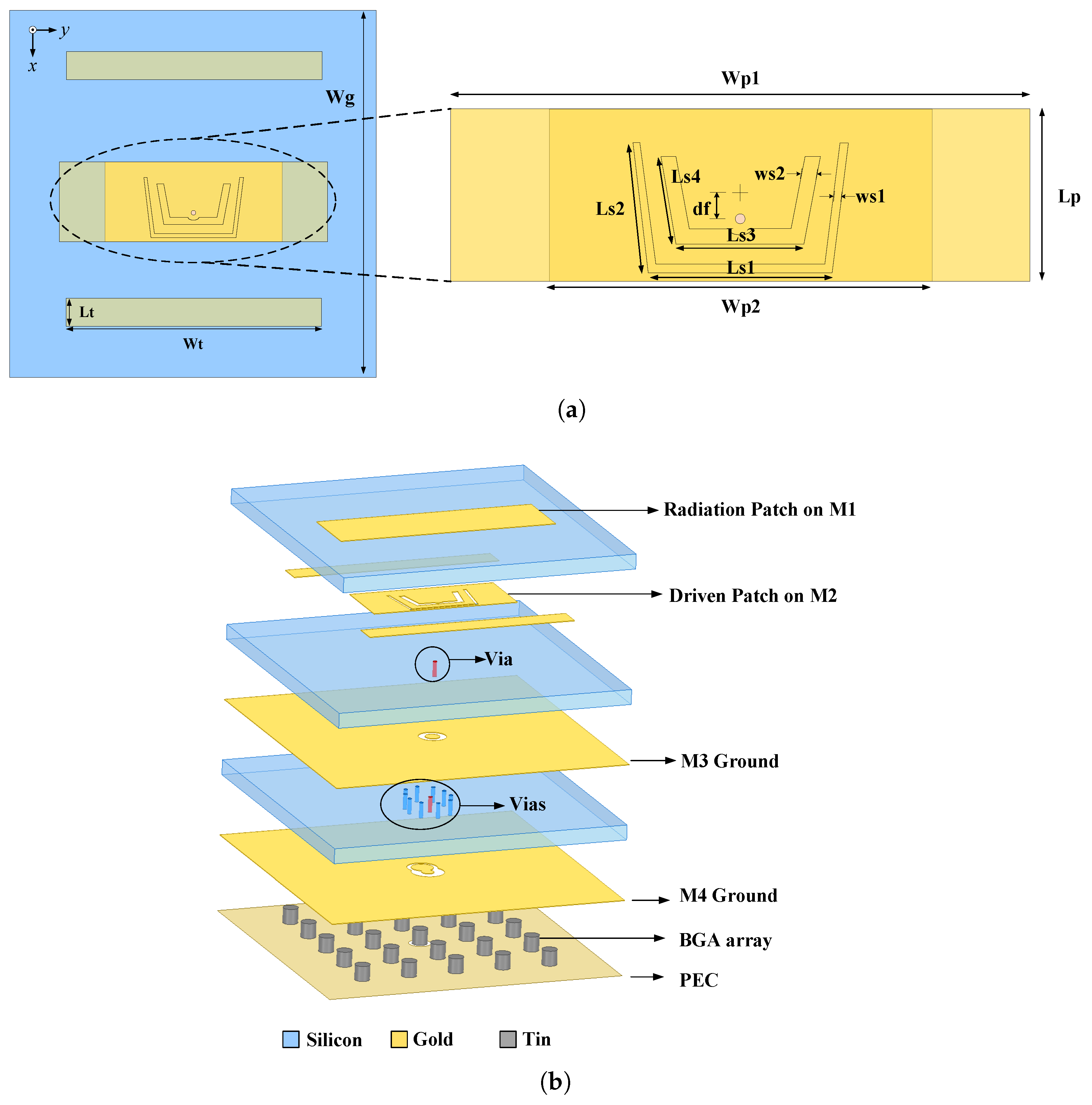
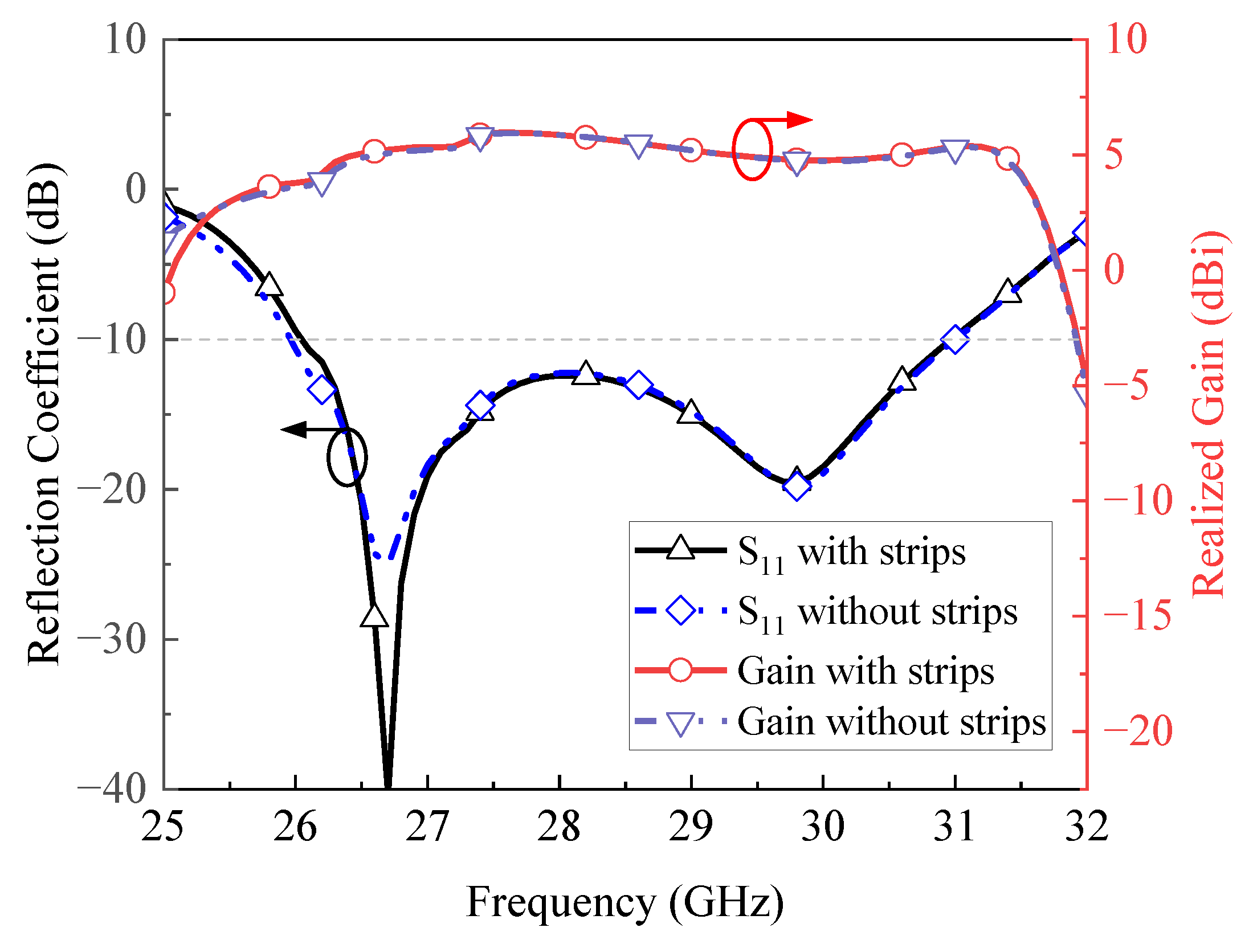
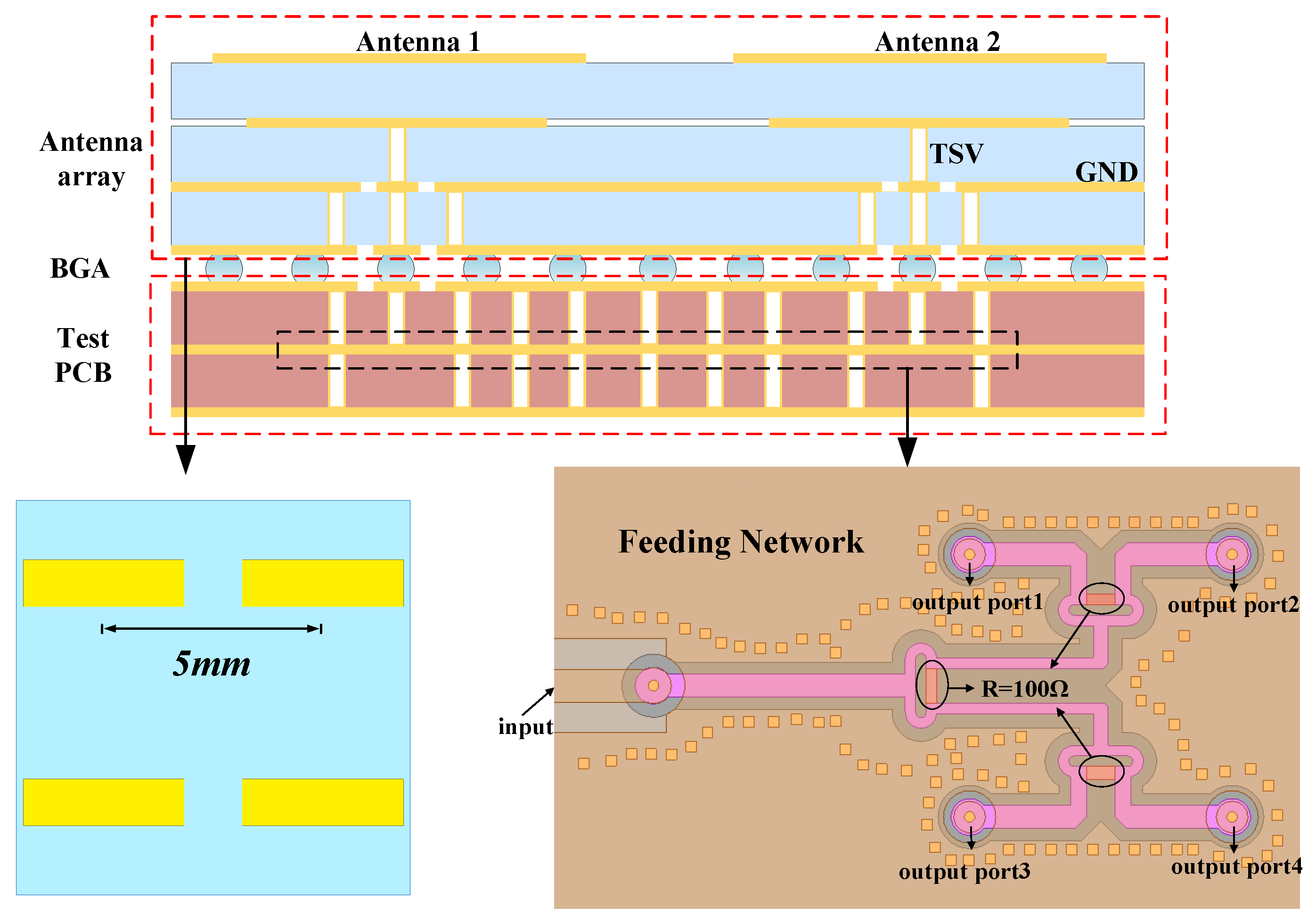
This section introduces the structure of the antenna unit, considering the fabrication and measurement requirements. A top view of the unit structure is shown in Figure 12a, and Table 1 lists the relevant parameters for the antenna design. In the exploded view in Figure 12b, the antenna consists of three layers of silicon and four layers (M1 to M4) of gold, with a total size of . The top patch is on M1 and the bottom patch fed by TSV is on M2. M3 and M4 are grounded with slotted isolation rings. The ball grid array (BGA) with a pitch of 0.8 mm interconnected with the print circuit board (PCB) is under the M4 layer, where the signal is fed from the central solder ball. It should be noted that, in order to meet the manufacturing rules for metal bonding between silicon wafers and ensure the mechanical stability of products, two strip metal shapes are added to the M2, which has little impact on the antenna performance, as shown in Figure 13.
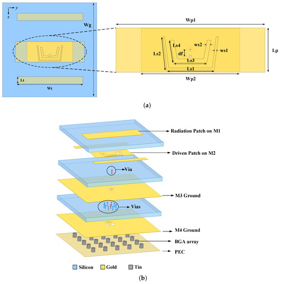
Figure 12.
Configuration of the proposed antenna unit. (a) Top view; (b) exploded view.

Table 1.
Dimensions of the proposed antenna. (Unit: mm).
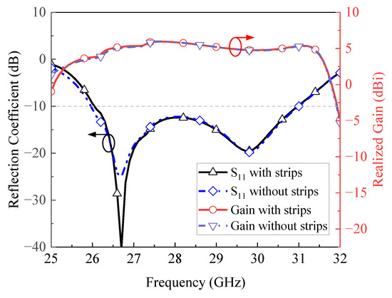
Figure 13.
Comparison of the antenna’s performance with/without strips on M2.
3. Fabrication and 2 × 2 Array Structure
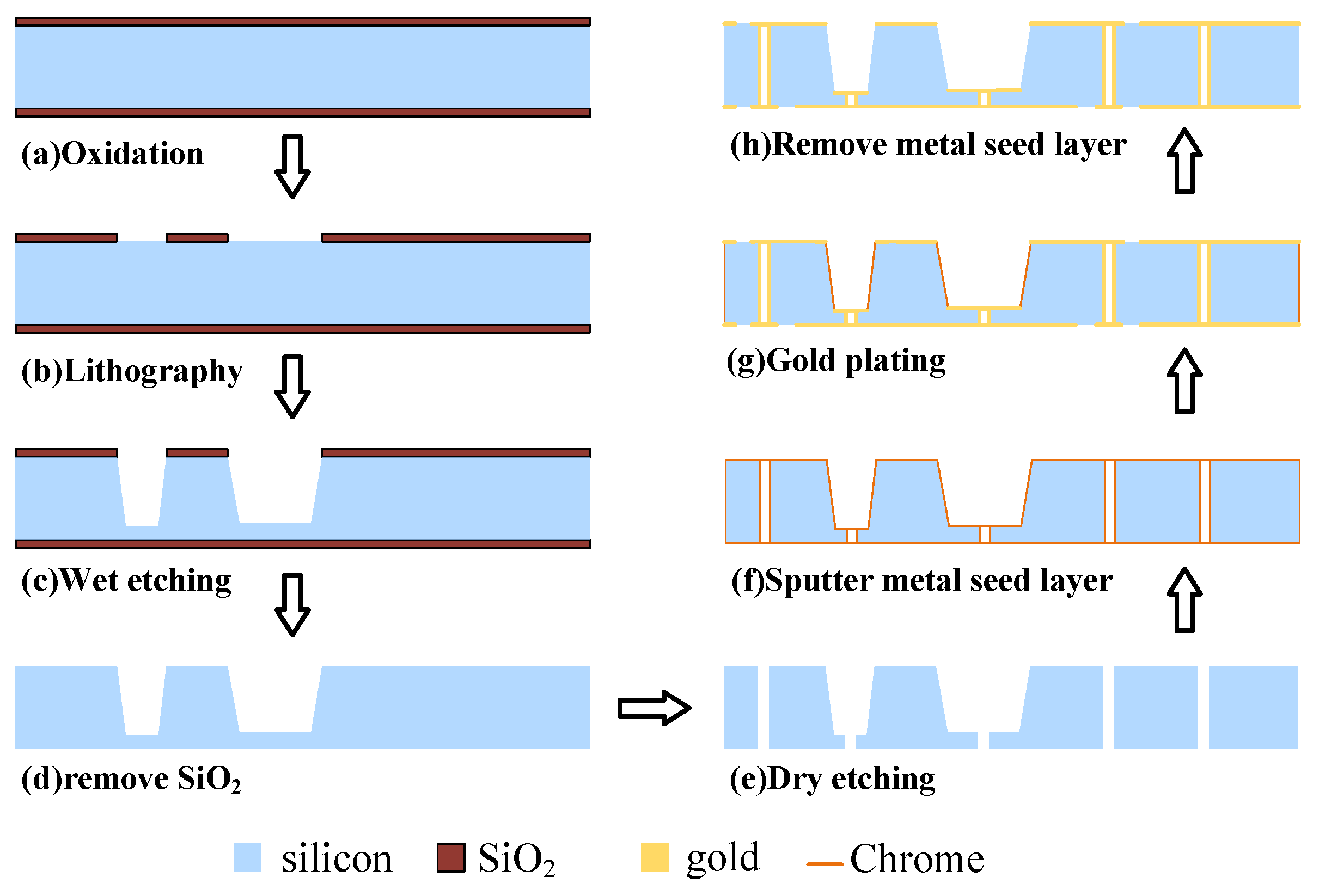
The proposed antenna was manufactured using bulk silicon micromachining and wafer-level assembly processes. Specifically, the bulk silicon process refers to the process of obtaining a certain shape of through groove, blind groove, or through vias on a certain thickness of silicon wafer using etching technologies. After etching, a gold layer with a thickness of 3 m was electroplated on each side of a wafer, and the process flow is shown in Figure 14. Then, high-precision wafer-level bonding was achieved between each layer of silicon wafers using gold, and there is a 10 m gold layer between the formed silicon wafers.
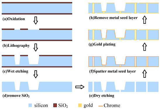
Figure 14.
Flow of the silicon bulk micromachining process.
To validate the antenna performance, a 2 × 2 array is designed with the feed network on PCB. Due to the layout of other active chips and the scanning performance of phased arrays, the unit spacing is designed to be 5 mm (0.47). The PCB contains two layers of substrate (Arlon AD300A, , ) and three layers of metal. In order to achieve equal amplitude feeding of units while ensuring signal transmission quality, a strip-line Wilkinson power division network was designed. Figure 15 shows a cross-section view of the whole 2 × 2 array structure for measurement. The antenna fabricated on silicon is bonded to the PCB through BGA which provides reliable interconnection.

Figure 15.
The assembled array and PCB feeding network.
4. Results and Discussion
Figure 16a shows a photograph of the fabricated antenna unit and subarray. The antennas bonded on the PCB through BGA are fixed on a metal base through the conductive adhesive. SMA connectors are installed on the side of the metal base for connection to coaxial transmission lines. Figure 16b shows a side view and a partial zoom-in zone of the BGA pattern after bonding. The shapes of the solder balls have a good consistence.
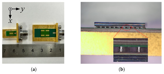
Figure 16.
(a) Fabricated antenna unit and array. (b) Detail photograph of BGA.
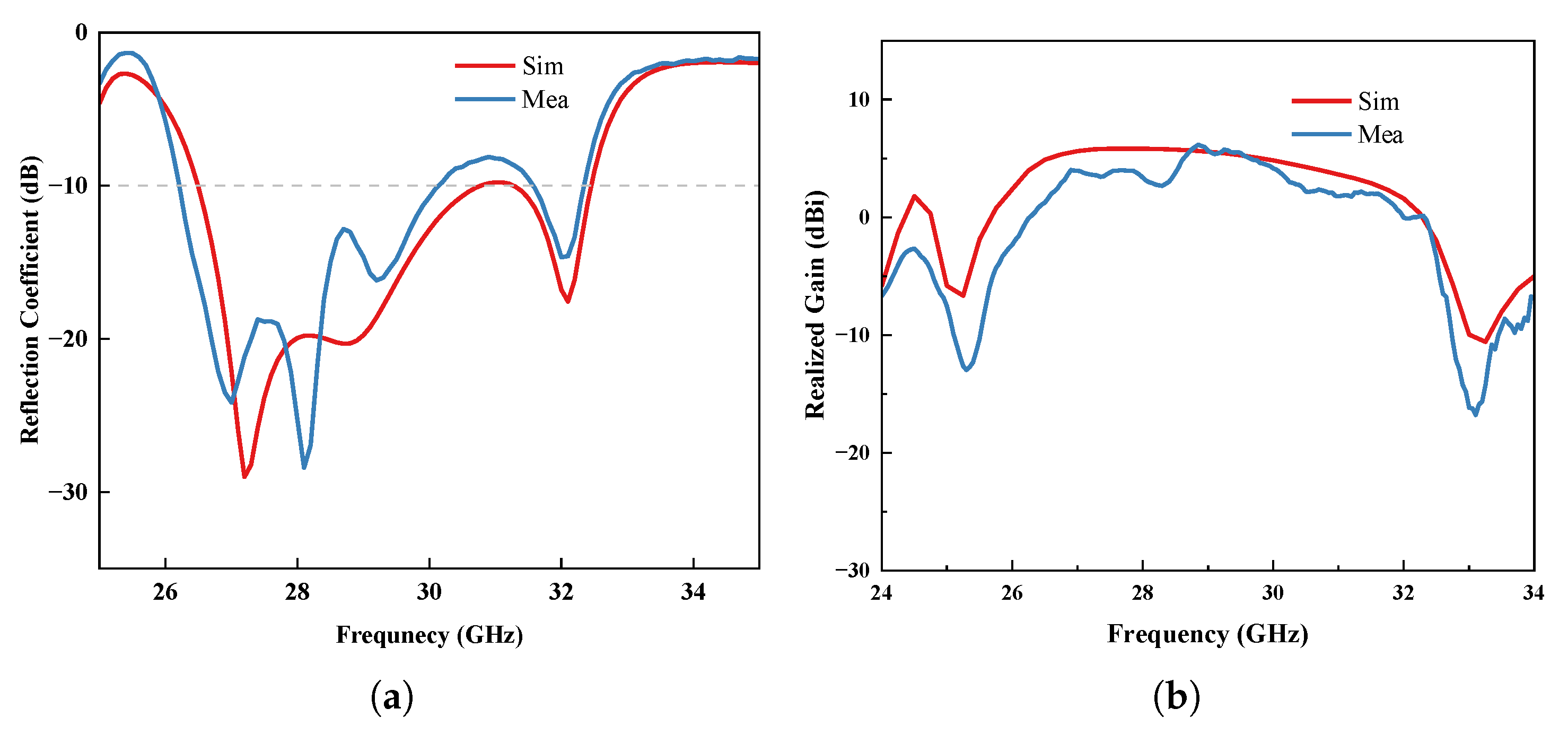
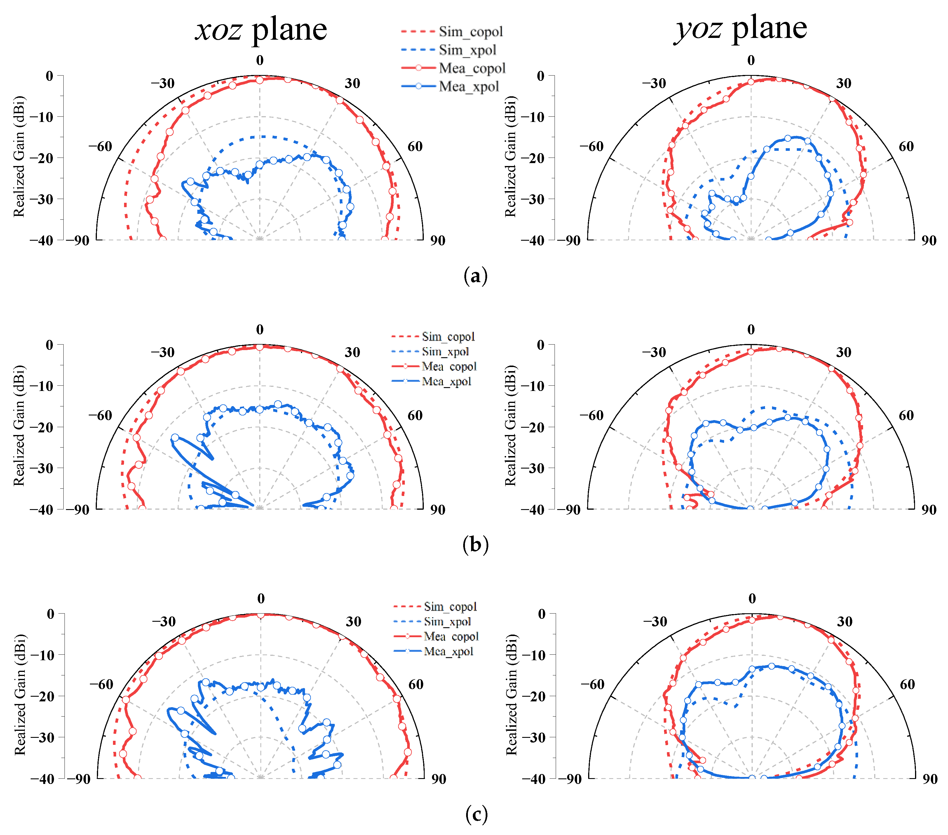
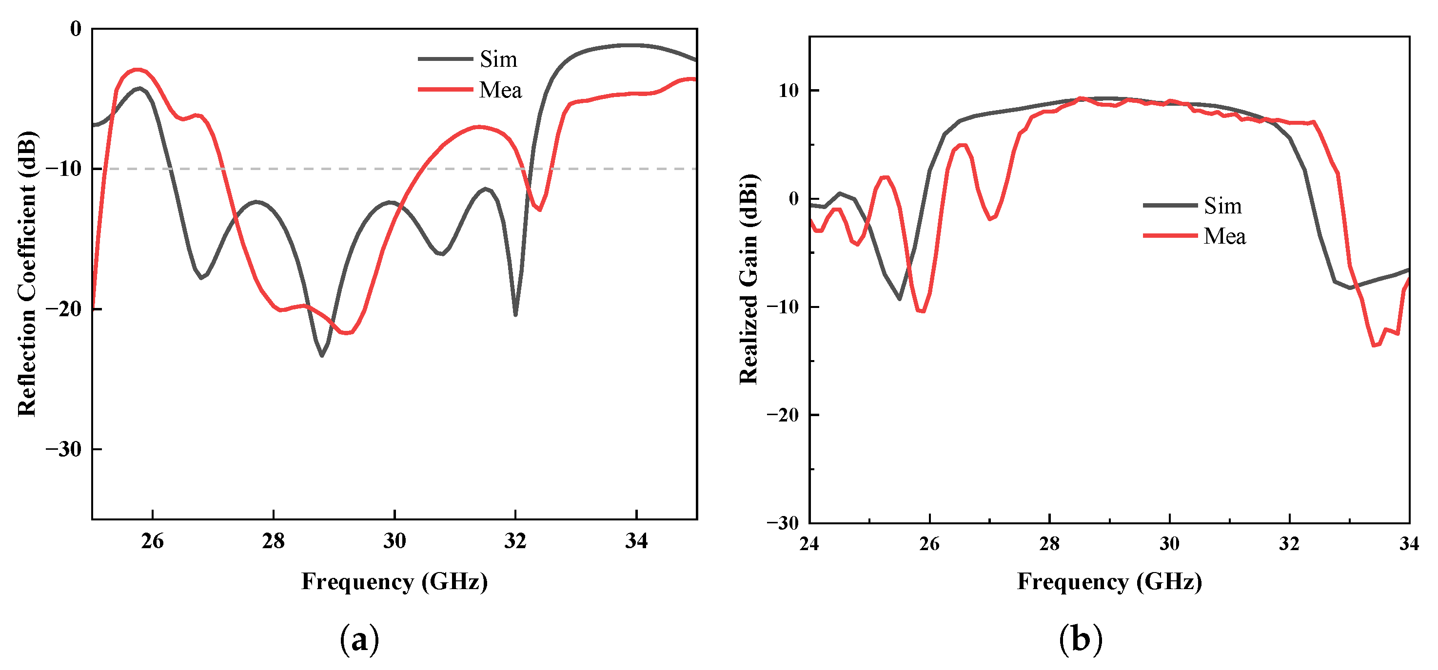
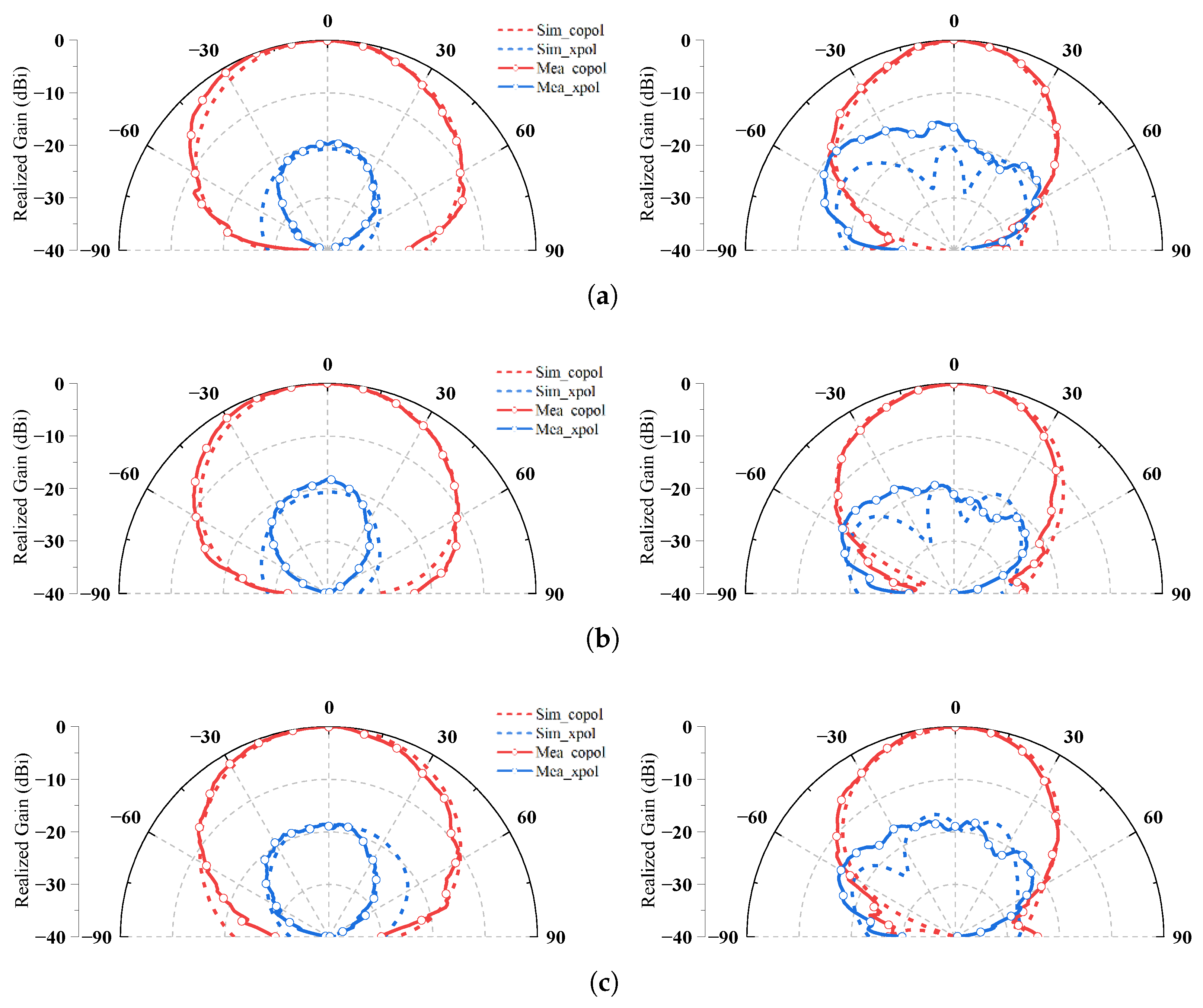
The antenna was tested in a microwave chamber. Figure 17a,b show the simulated and measured results of the reflection coefficient and boresight gain of the unit. The simulated impedance bandwidth ( dB) was from 26.5 GHz to 30.7 GHz, while the measured bandwidth was from 26.2 to 30.1 GHz. The measured gain fluctuated to some extent, but the trend of variation versus frequency was consistent with the simulated one. Figure 18 shows the simulated and measured normalized radiation patterns of the antenna unit in the and planes at 28, 29, and 30 GHz. Due to the testing conditions, only the frontal radiation was measured. The simulated and measured patterns were in good agreement.
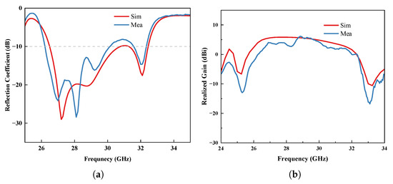
Figure 17.
Simulated and measured results. (a) S11; (b) boresight gain.
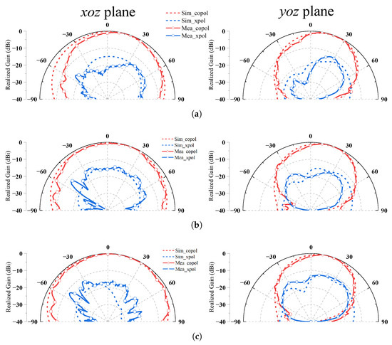
Figure 18.
Simulated and measured normalized radiation patterns of the proposed antenna unit. (a) 28 GHz; (b) 29 GHz; (c) 30 GHz.
The simulated and measured results of the array were in rough agreement, as shown in Figure 19. In addition to the frequency shift, note that an unexpected measured gain null occurred near 27 GHz and the reflection coefficient showed a peak. Consequently, the impedance bandwidth decreased compared with the simulated result. This discrepancy between the measured and simulated results of the array antenna was probably due to multiple factors. First, the TSV fabrication had a significant impact on the performance of the devices. Second, there may have been a slight misalignment between the silicon wafer and the PCB. Third, the material properties of silicon and the substrate for the test PCB were different from those used for simulation. All the above-mentioned factors could have contributed to the discrepancy, and more samples are needed to confirm the cause. The simulated and measured normalized radiation patterns of the subarray in the xoz and yoz planes at 28.5, 29.5, and 30.5 GHz are shown in Figure 20, which also shows a good agreement.
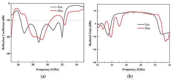
Figure 19.
Simulated and measured results of the array. (a) S11; (b) boresight gain.
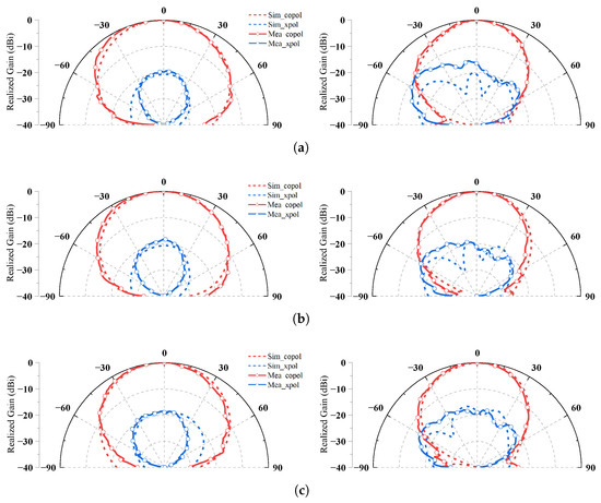
Figure 20.
Simulated and measured normalized radiation patterns of the array. (a) 28.5 GHz; (b) 29.5 GHz; (c) 30.5 GHz.
Table 2 shows a performance comparison between our design and the micromachined antennas in the previously reported articles. Our proposed antennas with wide band and high gain can be integrated in a 3-D manner with other components. The compact size can be used in highly integrated multi-functional systems.
Table 2.
Comparisons of the micromachined antennas on high- substrates.
5. Conclusions
In this paper, a wideband stacked patch antenna consisting of three HRSi substrates was proposed. The design approach was demonstrated step by step with the guidance of CMA. The antenna unit and 2 × 2 subarray operating at Ka-band were fabricated through bulk silicon micromachining and wafer bonding processes for validation. The measured results showed a bandwidth of 13.8% and 11.4% for the antenna unit and the 2 × 2 array, with a boresight gain of 6.1 dBi and 9.3 dBi, respectively. With this enhanced performance, a cost-effective and practical AiP design on silicon, which has the advantages of high integration and mechanical reliability, can be used for highly integrated millimeter-wave phased arrays.
Author Contributions
Model design and fabrication design, Y.Z.; simulation, validation, and model analysis, L.L.; simulation and fabrication, Y.H.; validation, supervision, Y.X.; supervision, H.S. All authors have read and agreed to the published version of the manuscript.
Funding
This research was funded by the National Natural Science Foundation of China grant number 62001522.
Data Availability Statement
Data are contained within the article.
Conflicts of Interest
Author Yu Zhao and Yali Hu are employed by the company The 13th Research Institute of China Electronics Technology Group Corporation. The remaining authors declare that the research was conducted in the absence of any commercial or financial relationships that could be construed as a potential conflict of interest.
References
- Zhang, Y.; Mao, J. An Overview of the Development of Antenna-in-Package Technology for Highly Integrated Wireless Devices. Proc. IEEE 2019, 107, 2265–2280. [Google Scholar] [CrossRef]
- Cohen, E.; Ruberto, M.; Cohen, M.; Degani, O.; Ravid, S.; Ritter, D. A CMOS Bidirectional 32-Element Phased-Array Transceiver at 60 GHz With LTCC Antenna. IEEE Trans. Microw. Theory Tech. 2013, 61, 1359–1375. [Google Scholar] [CrossRef]
- Zhang, Y.P.; Sun, M.; Chua, K.M.; Wai, L.L.; Liu, D. Antenna-in-Package Design for Wirebond Interconnection to Highly Integrated 60-GHz Radios. IEEE Trans. Antennas Propagat. 2009, 57, 2842–2852. [Google Scholar] [CrossRef]
- Kam, D.G.; Liu, D.; Natarajan, A.; Reynolds, S.; Chen, H.C.; Floyd, B.A. LTCC Packages With Embedded Phased-Array Antennas for 60 GHz Communications. IEEE Microw. Wirel. Compon. Lett. 2011, 21, 142–144. [Google Scholar] [CrossRef]
- Liu, D.; Gu, X.; Baks, C.W.; Valdes-Garcia, A. Antenna-in-Package Design Considerations for Ka-Band 5G Communication Applications. IEEE Trans. Antennas Propagat. 2017, 65, 6372–6379. [Google Scholar] [CrossRef]
- Gu, X.; Liu, D.; Baks, C.; Tageman, O.; Sadhu, B.; Hallin, J.; Rexberg, L.; Valdes-Garcia, A. A Multilayer Organic Package with 64 Dual-Polarized Antennas for 28 GHz 5 G Communication. In Proceedings of the 2017 IEEE MTT-S International Microwave Symposium (IMS), Honololu, HI, USA, 4–9 June 2017; pp. 1899–1901. [Google Scholar] [CrossRef]
- Kam, D.G.; Liu, D.; Natarajan, A.; Reynolds, S.K.; Floyd, B.A. Organic Packages With Embedded Phased-Array Antennas for 60-GHz Wireless Chipsets. IEEE Trans. Compon. Packaging Manuf. Technol. 2011, 1, 1806–1814. [Google Scholar] [CrossRef]
- Wojnowski, M.; Wagner, C.; Lachner, R.; Bock, J.; Sommer, G.; Pressel, K. A 77-GHz SiGe Single-Chip Four-Channel Transceiver Module with Integrated Antennas in Embedded Wafer-Level BGA Package. In Proceedings of the 2012 IEEE 62nd Electronic Components and Technology Conference, San Diego, CA, USA, 29 May–1 June 2012; pp. 1027–1032. [Google Scholar] [CrossRef]
- Chen, Z.; Guan, L.T.; Wee Ho, D.S.; Bhattacharya, S. Millimeter-Wave Antenna in Fan-Out Wafer Level Packaging for 60 GHz WLAN Application. In Proceedings of the 2018 IEEE 68th Electronic Components and Technology Conference (ECTC), San Diego, CA, USA, 29 May–1 June 2018; pp. 331–336. [Google Scholar] [CrossRef]
- Zhang, Y.P.; Liu, D. Antenna-on-Chip and Antenna-in-Package Solutions to Highly Integrated Millimeter-Wave Devices for Wireless Communications. IEEE Trans. Antennas Propagat. 2009, 57, 2830–2841. [Google Scholar] [CrossRef]
- Chang, L.; Zhang, Z.; Li, Y.; Wang, S.; Feng, Z. Air-Filled Long Slot Leaky-Wave Antenna Based on Folded Half-Mode Waveguide Using Silicon Bulk Micromachining Technology for Millimeter-Wave Band. IEEE Trans. Antennas Propagat. 2017, 65, 3409–3418. [Google Scholar] [CrossRef]
- Hacker, J.; Hillman, C.; Papavasiliou, A.; Kim, C.G.; Abbaspour-Tamijani, A.; Kim, C.Y.; Kang, D.W.; Rebeiz, G. A 16-Element Transmit/Receive Q-Band Electronically Steerable Subarray Tile. In Proceedings of the 2012 IEEE/MTT-S International Microwave Symposium Digest, Montreal, QC, Canada, 17–22 June 2012; pp. 1–3. [Google Scholar] [CrossRef]
- Shariff, D.; Marimuthu, P.C.; Hsiao, K.; Asoy, L.; Yee, C.L.; Oo, A.K.; Buchanan, K.; Crook, K.; Wilby, T.; Burgess, S. Integration of Fine-Pitched Through-Silicon Vias and Integrated Passive Devices. In Proceedings of the 2011 IEEE 61st Electronic Components and Technology Conference (ECTC), Lake Buena Vista, FL, USA, 31 May–3 June 2011; pp. 844–848. [Google Scholar] [CrossRef]
- Yong-zhi, Z.; Shao-dong, W. A Novel 3D T/R Module with MEMS Technology. In Proceedings of the 2016 International Conference on Integrated Circuits and Microsystems (ICICM), Chengdu, China, 23–25 November 2016; pp. 286–289. [Google Scholar] [CrossRef]
- Bouayadi, O.E.; Dussopt, L.; Lamy, Y.; Dehos, C.; Ferrandon, C.; Siligaris, A.; Soulier, B.; Simon, G.; Vincent, P. Silicon Interposer: A Versatile Platform towards Full-3D Integration of Wireless Systems at Millimeter-Wave Frequencies. In Proceedings of the 2015 IEEE 65th Electronic Components and Technology Conference (ECTC), San Diego, CA, USA, 26–29 May 2015; pp. 973–980. [Google Scholar] [CrossRef]
- Papapolymerou, I.; Franklin Drayton, R.; Katehi, L. Micromachined Patch Antennas. IEEE Trans. Antennas Propag. 1998, 46, 275–283. [Google Scholar] [CrossRef]
- Gauthier, G.; Courtay, A.; Rebeiz, G. Microstrip Antennas on Synthesized Low Dielectric-Constant Substrates. IEEE Trans. Antennas Propagat. 1997, 45, 1310–1314. [Google Scholar] [CrossRef]
- James, J.R.; Hall, P.S. Handbook of Microstrip Antennas; Institution of Electrical Engineers, Ed.; IEE Electromagnetic Waves Series; Peregrinus: London, UK, 1989. [Google Scholar]
- Pozar, D. Considerations for Millimeter Wave Printed Antennas. IEEE Trans. Antennas Propagat. 1983, 31, 740–747. [Google Scholar] [CrossRef]
- Carver, K.; Mink, J. Microstrip Antenna Technology. IEEE Trans. Antennas Propagat. 1981, 29, 2–24. [Google Scholar] [CrossRef]
- Chen, Y.; Wang, C.F. Characteristic Modes: Theory and Applications in Antenna Engineering, 1st ed.; Wiley: Hoboken, NJ, USA, 2015. [Google Scholar] [CrossRef]
- Tong, K.F.; Luk, K.M.; Lee, K.F.; Lee, R. A Broad-Band U-Slot Rectangular Patch Antenna on a Microwave Substrate. IEEE Trans. Antennas Propagat. 2000, 48, 954–960. [Google Scholar] [CrossRef]
- Waterhouse, R. Design of Probe-Fed Stacked Patches. IEEE Trans. Antennas Propagat. 1999, 47, 1780–1784. [Google Scholar] [CrossRef]
- Milligan, T. Antenna Designer’s Notebook - Wheeler and Fano Impedance Matching. IEEE Antennas Propag. Mag. 2007, 49, 116–119. [Google Scholar] [CrossRef]
- Singh, V. Ka-Band Micromachined Microstrip Patch Antenna. IET Microw. Antennas Propag. 2010, 4, 316. [Google Scholar] [CrossRef]
- Pan, B.; Yoon, Y.k.; Ponchak, G.E.; Allen, M.G.; Papapolymerou, J.; Tentzeris, M.M. Analysis and Characterization of a High-Performance Ka-Band Surface Micromachined Elevated Patch Antenna. IEEE Antennas Wirel. Propag. Lett. 2006, 5, 511–514. [Google Scholar] [CrossRef]
- Mirzajani, H.; Nasiri, M.; Ghavifekr, H.B. A New Design of MEMS-Based Wideband Frequency Reconfigurable Microstrip Patch Antenna. In Proceedings of the 2012 8th International Symposium on Mechatronics and Its Applications, Sharjah, United Arab Emirates, 10–12 April 2012; pp. 1–6. [Google Scholar] [CrossRef]
- Watanabe, A.O.; Ali, M.; Zhang, R.; Ravichandran, S.; Kakutani, T.; Raj, P.M.; Tummala, R.R.; Swaminathan, M. Glass-Based IC-Embedded Antenna-Integrated Packages for 28-GHz High-Speed Data Communications. In Proceedings of the 2020 IEEE 70th Electronic Components and Technology Conference (ECTC), Orlando, FL, USA, 3–30 June 2020; pp. 89–94. [Google Scholar] [CrossRef]
- Jin, C.; Sekhar, V.N.; Bao, X.; Chen, B.; Zheng, B.; Li, R. Antenna-in-Package Design Based on Wafer-Level Packaging with Through Silicon Via Technology. IEEE Trans. Compon. Packag. Manufact. Technol. 2013, 3, 1498–1505. [Google Scholar] [CrossRef]
- Huang, Y.S.; Zhou, L.; Mao, J.F.; Xu, Q. A W-Band High Radiation Efficiency With BCB-Air Cavity-Backed Antenna Based on Through Silicon Ring Trench. IEEE Antennas Wirel. Propag. Lett. 2022, 21, 1955–1959. [Google Scholar] [CrossRef]


Disclaimer/Publisher’s Note: The statements, opinions and data contained in all publications are solely those of the individual author(s) and contributor(s) and not of MDPI and/or the editor(s). MDPI and/or the editor(s) disclaim responsibility for any injury to people or property resulting from any ideas, methods, instructions or products referred to in the content. |
© 2023 by the authors. Licensee MDPI, Basel, Switzerland. This article is an open access article distributed under the terms and conditions of the Creative Commons Attribution (CC BY) license (https://creativecommons.org/licenses/by/4.0/).