1. Introduction
The mid-infrared spectral range (2.8–5.4 μm) is important for many applications of optical gas sensing [
1] such as medical diagnosis by breath analysis and for environmental protection by localizing leaks of toxic and harmful gases [
2]. Semiconductor heterostructures based on the narrow-gap InSb–InAs solid solutions system are very promising for the creation of light-emitting diodes operating in the atmospheric transparency window of 4.4–5.4 μm [
3,
4]. This spectral region contains the intense absorption bands of a number of nitrogenous chemical compounds (N
2O, NO, (CN)
2, HCN, etc.), which are of great interest for industrial gas analysis and the detection of some explosive and dangerous substances [
5]. It is known that the use of quantum dots (QDs) in the active region of laser diodes increases the quantum efficiency and the operating temperature of these devices [
6]. This opens up great opportunities for improving the design of mid-infrared optoelectronic devices. In contrast to well-studied wide-gap systems such as InAs/GaAs and InSb/InP, the energy band diagram of the narrow-gap InSb/InAs heterostructure exhibits a type II broken-gap heterojunction at each QD/matrix layer interface [
7]. This specific feature of the InSb/InAs nanoheterostructures raises the question of identifying radiative transitions assisted by quantum dots. Recently, the photoluminescent (PL) properties of heterostructures based on the InSb QD layers inserted into the n-InAs matrix were studied [
8]. A long-wave radiation was detected in the spectral range of 4–5 μm (0.25–0.3 eV) at low temperatures due to recombination transitions involving quantum dot eigenstates. The electroluminescence (EL) study was performed for heterostructures based on a single layer of the InSb QDs buried in the p-InAs matrix [
9]. The EL spectra displayed positive luminescence when forward bias was applied and negative luminescence when reverse external bias was applied to the structure under study in the temperature range of
T = 77–300 K. Interband radiative recombination caused by the lightly doped p-InAs bulk was observed at both biases. Only a small contribution of interface-induced luminescence indicated the presence of the InSb QDs. In our current work, we present the results of the study of electroluminescence owing to radiative transitions involving quantum dot eigenstates. To fulfill this purpose, type II broken-gap heterostructures with a single layer of the InSb QDs located directly on the interface of the p-InAs/n-InAs junction were manufactured.
2. Materials and Methods
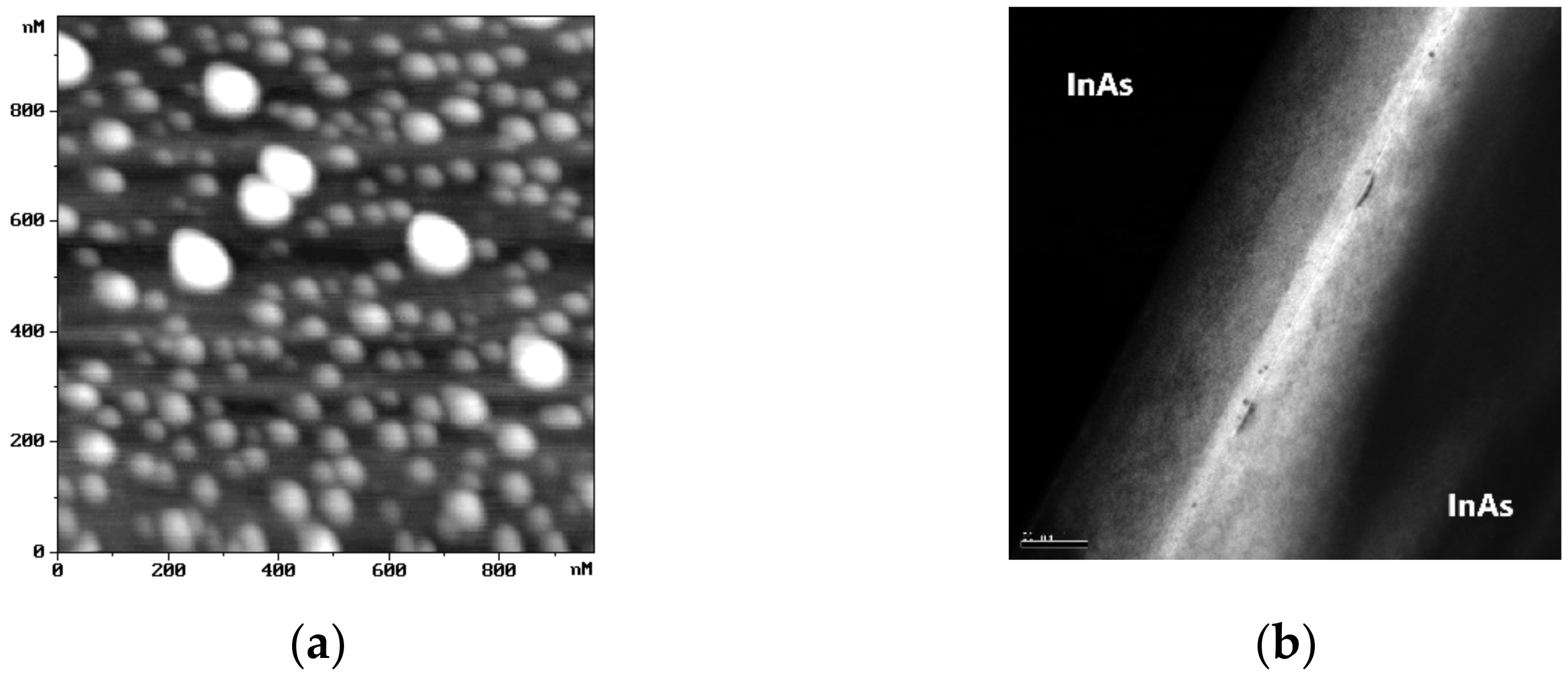
Narrow-gap heterostructures containing one layer of InSb QDs embedded in the InAs matrix were obtained using a combined epitaxial growth technology. The samples under study were grown on p-InAs(001) substrates doped with an acceptor impurity (Mn) to a hole concentration of
p300~10
17 cm
−3 at
T = 300 K. At the first stage of the heterostructure fabrication, the InSb QDs array was deposited on the p-InAs substrate by means of liquid-phase epitaxy (
Figure 1a). The technique used for the QDs growth and study on their structural properties in the InAs/InSb system were reported elsewhere [
10,
11]. Arrays of QDs in the surface density range of 0.5–2 × 10
10 cm
−2 with a step of 2 × 10
9 cm
−2 were obtained. The layer of InSb QDs was further overgrown with an epitaxial layer of indium arsenide using metal-organic vapor phase epitaxy (MOVPE). The n-InAs capping layer was intentionally undoped. It exhibited n-type conductivity with an estimated residual electron concentration of
n300~6∙10
16 cm
−3 at
T = 300 K. The presence of the InSb QD arrays buried in the InAs matrix formed was confirmed by transmission electron microscopy investigations (
Figure 1b). None of the structures obtained exhibited luminescence from QDs, except for samples with a limiting density of 2 × 10
10 cm
−2. Therefore, the two most typical representatives from the whole series of samples were selected for the EL study (see
Table 1). Additionally, the p-InAs/n-InAs structure (without the QD layer) was chosen as a test sample (see sample A in
Table 1). It was obtained together with samples B and C in a single MOVPE process. Because epitaxial overgrowth was carried out using undoped compounds, it is possible to almost exclude the diffusion of the acceptor impurity across the p-InAs/n-InAs heterointerface from the p-InAs part of the matrix into the n-InAs layer being overgrown. Thus, a metallurgical p-n junction was formed inside the InAs matrix, at the interface of which the InSb QDs layer was located (see sample B and C in
Table 1).
Samples for EL studies were performed as mesa diodes of 500 × 500 μm in size with a wide contact to the substrate side and a point contact to the upper epitaxial layer. A round mesa fabricated by standard photolithography and selective wet chemical etching had the diameter of D~300 μm; whereas, the point contact diameter was d~50 μm. The studied mesa diodes were mounted on the TO-18 package and located with a substrate side to the metal case. In this design, the radiation emerging from the structure was detected from the side of the capping epitaxial layer. The EL spectra were recorded using an automated setup based on a DK-480 monochromator (CVI Laser Corp., Albuquerque, NM, USA) with a diffraction grating of 150 lines/mm, an InSb photovoltaic detector cooled by liquid nitrogen (Judson Co, Montgomeryville, PA, USA), and an SR-810 lock-in amplifier (Stanford Research Systems Inc., Sunnyvale, CA, USA). The samples were supplied by rectangular current pulses with a duty cycle of η = 50% and a frequency of f = 512 Hz, both with forward and reverse external bias. The forward bias corresponds to the case where the positive potential was applied to the p-InAs substrate; whereas, the negative one was applied to the upper n-InAs layer. Therefore, reverse bias has the opposite configuration of polarities. The pulse amplitude of the driving current (i) was varied from 20 mA to 200 mA.
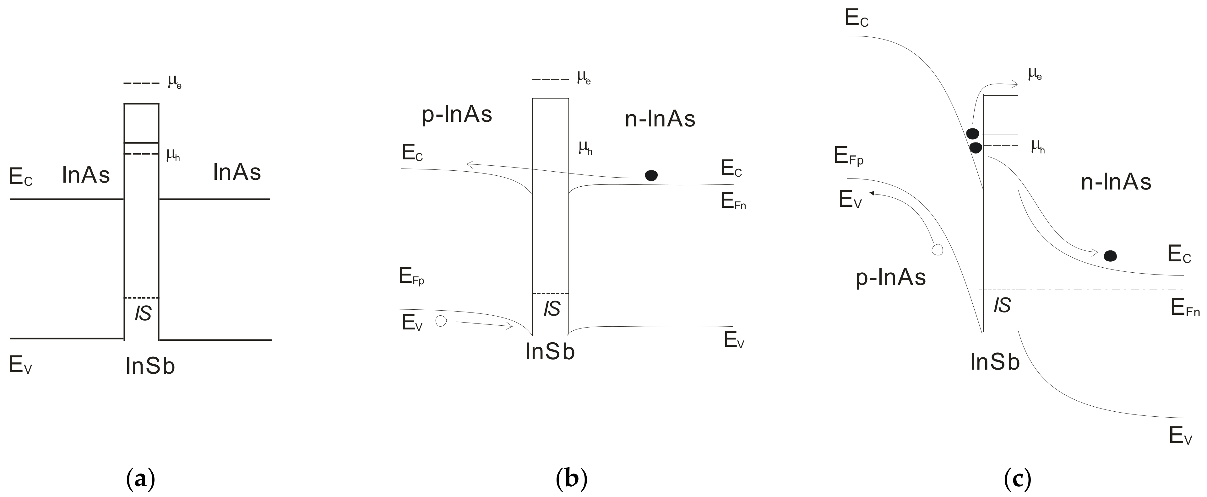
To analyze the obtained EL spectra, preliminary calculations of the band energy diagrams of the heterostructures studied in the experiment were carried out. Estimation of the energy spectrum of quantum-size structures was performed using available resources [
12]. For instance, a single InSb QD can be represented as a narrow one-dimensional potential well with a set of localized levels (
Figure 2a). This makes it possible to determine the energy levels for electrons and holes depending on the well width, material compositions and parameters of adjacent semiconductor compounds. It can be seen from the figure that the ground hole level of the InSb QD (μ
h) is situated in energy above the bottom of the conduction band of the InAs matrix layer due to the peculiarity of the type II broken-gap heterojunction in the InSb-InAs system. As was shown in [
13], structural crystalline defects in indium arsenide can create acceptor states (IS) on the surface of a semiconductor.
3. Results
EL spectra at room temperature displayed similar features for all structures under the study on forward bias applied (
Figure 3a). The typical EL spectrum contained one pronounced emission band with an intensity maximum near
hν300(+) = 0.36 eV and FWHM = 48 meV, which corresponded to interband radiative transitions in the bulk of indium arsenide [
14]. Additional emission bands can be distinguished near
hνIS = 0.31 eV as a shoulder on the low-energy slope of the main EL band. At forward bias (
Figure 2b), potential barriers near the InAs/InSb interface appear on the moving path of electrons in an external electric field from the populated conduction band of n-InAs to the unfilled conduction band of p-InAs. These barriers are induced by the QDs energy band structure and interface states at the heteroboundary between the matrix layers. It should be emphasized that no other radiative recombination transitions involving impurity states with an activation energy of less than 30 meV were detected, which can be explained by the depletion of shallow levels due to their thermal warming at
T = 300 K.
At reverse bias (
Figure 2c), the shapes of the EL spectra at room temperature for samples with and without QDs were radically different from each other (
Figure 3b). The EL spectrum for the p-InAs/n-InAs structure showed an emission band in the vicinity of
hν300(−) = 0.36 eV, reversed in phase by 180° relative to the zero-intensity level, i.e., negative luminescence was observed in the bulk of p-InAs [
9,
15]. Together with this band, a weak peak of positive EL was found at photon energy
hνIS = 0.31 eV. Contrary to sample A, the heterostructures with InSb QDs (p-InAs/InSb/n-InAs) demonstrated exclusively positive luminescence. Note that these EL spectra contain only one emission band and exactly with an intensity maximum in the vicinity of the photon energy of 0.31 eV. Radiation in the range of photon energy close to the InAs band gap was not detected for samples B and C at all. The space charge region is shunted by the ohmic contact of the type II broken-gap heterojunction due to the fact that the hole levels of the InSb QD are situated in energy above the conduction band of the InAs matrix layers. The main drop in external bias can be expressed as a linear slope in the region of the flat energy bands in the InAs layer that provides conditions for the free movement of electrons to the unfilled conduction band of the n-InAs and further to a metal contact without any potential barriers in their path. In this way, the process of extraction of charge carriers from the depleted regions can be significantly suppressed. A similar effect of negative luminescence suppression was recently observed for heterostructures with an ultrathin oxide layer separating the surfaces of two contacting semiconductors, which are forming a type II broken-gap heterojunction under conservation of the levels of localized states on the surface of indium arsenide [
16]. Thus, radiative recombination transitions are realized with the participation of the interface level (IS) for any direction of the injection current (both forward and reverse biases) that is expressed in the presence of an emission band with unchanged polarity in the EL spectrum. Therefore, the
hνIS emission band observed at room temperature can be ascribed to radiative transitions involving the surface states at the p-InAs/n-InAs heterointerface which are placed 50 meV above the top of the InAs valence band.
As the temperature is lowered to
T = 77 K, the contribution of radiative recombination transitions with the participation of impurity states in p-InAs, which have an activation energy greater than the energy of thermal level smearing (
kT77~6 meV), becomes noticeable. The EL spectra for all the studied samples contained two distinct emission bands
hν77 = 0.408 eV and
hν77A = 0.376 eV upon application of forward external bias (
Figure 4). The high-energy band (
hν77) can be attributed to interband radiative transitions in InAs [
14]. The energy distance of the low-energy band
hν77A from the high-energy band was 32 meV, which points to radiative recombination transitions associated with impurity acceptor states of Mn situated in the forbidden gap of InAs [
17]. Furthermore, the presence of an additional emission band is assumed, which can be revealed as a shoulder on the low-energy slope of the EL spectrum with an emission maximum near 0.35 eV. We suppose that it can be ascribed to radiative transitions involving interface states (Δ
hν77(IS)~58 meV).
The EL measurements revealed different behavior in intensity of the emission bands with increasing driving current for the samples under study depending on the surface density of the InSb QDs at the
p-n junction interface. For sample A (without QDs) and sample B (with a low concentration of QDs), the dominance of the emission band
hν77A was retained over the entire range of driving currents (
Figure 4a). For sample C (with a high concentration of QDs), a redistribution of intensity between the EL bands was observed, when the dominance of the low-energy band
hν77A at low injection levels (
i < 50 mA) was replaced by the advantage of the high-energy band
hν77 at higher injection levels (
Figure 4b). In this case, the current dependence of EL intensity for the
hν77 band that occurred by interband radiative transitions in indium arsenide was changing within equal range for all samples. In other words, an increase in the surface density of nano-objects at the interface led to a decrease in the contribution of radiative transitions involving impurity acceptor states of p-InAs to the total EL spectrum. According to the energy diagram shown in
Figure 1b, the appearance of a space charge region on the p-InAs side near the heterointerface prevents electrons from penetrating into the region of flat bands, where radiative recombination with the participation of impurity levels takes place.
When reverse bias was applied to the heterostructures under study, the EL spectra at
T = 77 K showed no emission band corresponding to interband transitions in InAs (
Figure 5), as well as at room temperature performance. This characteristic feature of EL behavior at low temperatures was previously observed for heterostructures with the InSb QDs layer at the type II broken-gap InAs/InSb heterointerface in the p-InAs matrix, where interband transitions began to manifest themselves as a negative luminescence at high pump levels only [
9]. The main emission band (
hνIS+Channel) in the EL spectra recorded at reverse bias had an asymmetric shape with a sharp high-energy edge and exhibited a “blue” shift; i.e., the spectral position of the EL peak was shifting towards higher photon energies with an increase in driving current (
Figure 6).
Different behavior should be distinguished between the “blue” shift for each dependence of the EL emission band on the current. A linear dependence of the
hνIS+SL(i) band for sample A was observed in the photon energy range from 0.345 eV to 0.358 eV in the current interval
i = 50–150 mA (
Figure 6, filled squares). Comparing the energy band diagram of sample A at reverse bias (not shown) and the photon energy range in which the shift of the band
hνIS+SL was observed, one can estimate the energy position of the interface level IS at low temperature. It turns out that the linear “blue” shift observed in the EL spectra for sample A is the result of radiative transitions from shallow impurity levels (
SL) formed by natural structural defects in the n-InAs capping layer to the interface level
IS. Then, an increase in the reverse bias will cause a gradual depletion of the donor levels in n-InAs near the heterojunction. According to our estimates, the level
IS was approximately 50 meV above the top of the InAs valence band at a low temperature (
T = 77 K), which is in good agreement with the experimental data obtained at room temperature (see above).
Note also that both dependences
hνIS+channel(i), which describe the “blue” shift for samples with QDs, demonstrated non-linear behavior and saturation at high pumping. The specific shape of these dependences was determined by the surface density of nano-objects at the InAs/InSb heterointerface. For sample C, with a high concentration of the InSb QDs at the interface (
nQD2 > 10
10 cm
−2), luminescence began to appear at a photon energy
hIS+channel = 0.366 eV (
Figure 6, filled circles). In this case, the range of motion of the given EL band from the high-energy side was limited by the value of the radiative transition energy
hνA = 0.376 eV (
Figure 6, open squares). In contrast to samples A and C, the curve ascribed to sample B, with a low concentration of QDs at the interface (
nQD < 10
10 cm
−2), occupies an intermediate position, representing the result of a superposition of the two extreme cases considered (
Figure 6, filled triangles). For this sample, the onset of luminescence was recorded at
hIS+channel = 0.348 eV, and the “blue” shift was saturated at a photon energy of 0.37 eV.
4. Discussion
This section will consider the emergence of the band
hνIS + channel and discuss its behavior. When reverse bias has been applied to the heterostructures with InSb QDs (samples B and C), a potential well on the p-InAs side near the InAs/InSb interface emerged as a result of bending in the conduction band (
Figure 2c). A 2D-electron channel is formed at the p-InAs/InSb heterojunction under increasing the external electric field due to the filling of the potential well with electrons [
18]. Then, there is the possibility of radiative recombination transitions from the quasi-Fermi level (
EFp) states of the electron channel to the interface states
IS [
19]. The quantum energy of such transitions can be described by the following expression
where
EIS and
EFp are the energy of the interface level and Fermi level position relative to the bottom of the InAs conduction band, respectively. With a further increase in the external bias and, consequently, the filling of the electron channel, the
EFp level is shifted upward in energy that will be expressed in the "blue" shift of the EL band corresponding to these transitions. The subsequent saturation of the observed shift with increasing driving current is explained by the fact that the filling of the electron channel continues until electrons leak through the potential barrier formed by the band gap of the InSb QD. An additional current flow channel is formed already with the participation of the QD electron states. Accordingly, samples with various QD concentrations at the interface demonstrate different saturation levels of the “blue” shift of the EL bands (see
Figure 6).
The appearance of the additional current flow channel upon application of a reverse bias enables filling of the eigenstates in the InSb QDs. Therefore, the EL spectra at low temperatures can contain the emission band corresponding to recombination transitions between localization levels in a quantum dot. The photon energy of such transitions can be estimated as
where
EQD is the band gap of the InSb binary compound,
δEQD is the deviation in the band gap of InSb due to internal compression strain in the InSb QD,
μe and
μh are the energies of the ground electron and hole levels of the InSb QD, respectively. The EL spectra of sample C exhibited the emission band in the region
hνQD = 0.270 eV with a half-width of about 60 MeV (
Figure 5b). Note that a sharp dip at the low-energy edge of the EL spectrum near a photon energy of 0.29 eV is associated with the absorption of optical radiation by CO
2 molecules (
λ = 4.27–4.29 μm) present in the laboratory atmosphere [
3,
5].
The spectral position of the
hνQD band agrees well with the experimental data obtained by measuring the PL spectra at T = 77 K for structures with InSb QDs in an InAs matrix grown by molecular beam epitaxy [
8]. It should be emphasized that the mentioned PL band was recorded only for structures with a surface density of nano-objects of
nQD > 2∙10
10 cm
−2. Because the intensity of EL radiation induced by transitions between localized levels in QDs also depends on the concentration of nano-islands, the band
hνQD was not detected for samples with lower surface density of the InSb QDs (
Figure 5a). In the EL spectra of sample C recorded at T = 300 K, the corresponding EL band was not observed either (
Figure 3b). This was caused by the fact that the presented measurements were carried out using an InSb photovoltaic detector with a long-wavelength cutoff
λ = 5.3 μm that did not allow the recording of luminescence with a photon energy less than 0.23 eV. Attempts to obtain electroluminescence in heterostructures with InSb QDs in an InAs-based matrix were undertaken by other scientific groups; however, the low surface density of nano-objects prevents interpretation of the observed emission band with a photon energy near 0.37 eV as radiative recombination involving the states of InSb QDs [
20]. It is highly likely that the claimed EL band is due to the participation of surface levels at the InAs/InSb heterointerface.


