Article

Compact Microstrip Line to Rectangular Waveguide Transition Using Corrugated Substrate Integrated Waveguide

Beijing Key Laboratory of Work Safety Intelligent Monitoring, School of Electronic Engineering, Beijing University of Posts and Telecommunications, Beijing 100876, China
*
Author to whom correspondence should be addressed.
Electronics 2023, 12(3), 614; https://doi.org/10.3390/electronics12030614
Submission received: 13 December 2022 / Revised: 18 January 2023 / Accepted: 18 January 2023 / Published: 26 January 2023
(This article belongs to the Section Microwave and Wireless Communications)

Abstract

:
To meet the packaging requirements of terahertz (THz) communication systems, a microstrip line (MSL) to rectangular waveguide (RWG) transition is proposed in this paper. In the transition, the MSL is connected to the corrugated substrate integrated waveguide (CSIW) by a tapered MSL for quasi-TEM to TE10-like mode conversion on substrate, which requires no via holes or shaped dielectric, and is easy to process in THz bands. Then, the CSIW is straightly connected to the RWG transformer and converted to standard RWG, resulting in a compact structure. The working principle of the proposed transition is analyzed, and the influence of several important parameters on the S-parameters of the transition is discussed. A single transition is designed for the 325–500 GHz operation, the S11 better than −14.5 dB and S21 better than −1.03 dB have been achieved in the entire frequency band.

1. Introduction

With the growing demands of ultra-fast wireless communications, the terahertz (THz) frequency band has drawn much attention because of the large available bandwidths [1]. THz RF systems are usually composed of independent devices. For example, THz mixers, power amplifiers, etc., use microstrip lines (MSLs) as transmission lines. Rectangular waveguides (RWGs) are used between different devices to ensure low loss connection in the systems. For the purpose of integration and packaging, MSL-to-RWG transitions are required.
MSL-to-RWG transitions can be divided into E-plane and H-plane transitions according to the relative positions of the two transmission lines. E-plane probes [2] have been extensively used because of their broadband performance, but for this type of transition, the MSL is placed perpendicular to the RWG, which requires extra waveguide bends when applied to inline applications. Meanwhile, several types of H-plane MSL-to-RWG transitions have been proposed in the previous research for inline applications.
In the first type of H-plane transitions, the multi-section ridge waveguide transformers with gradually decreasing heights are used to match the impedance between MSL and RWG [3,4,5]. They can realize broadband transitions with simple structures on the substrate, but the ridge waveguide sections of small widths are scaled to THz bands. The ridge widths are 1.651 mm in the K-band [3], and 1 mm in the Q-band [4], which will be 0.1 mm and 0.14 mm, respectively, at 300 GHz, making it difficult to process. In addition, the mechanical strength of the ridge and the electrical contact between MSL and ridge waveguide are not easy to guarantee.
The second type of transitions are based on electromagnetic coupling. The quasi-TEM mode wave of MSL propagates into the cavity and generates TE10 mode waves, the waveguide shorting wall and perfect magnetic conductor (PMC) are used to prevent backward radiation in [6] and [7], respectively. Their metallic parts are much simpler than that of ridge waveguides; however, similar to the working principle of E-plane probes, the part of the substrate above the cavity should not have a ground plane which requires double side printed circuits and increases fabrication costs. In [8], the MSL and the Empty substrate integrated waveguide (ESIW) are coupled through a circular gap and a cylindrical filament with the same center; the methodology is further applied to MSL-to-RWG transitions. In [9], the MSL-to-RWG transition is realized by through ground patch coupling, and a waveguide step is used for broadband matching. In [10], a radiation probe is employed for coupling. Wideband H-plane transitions can be achieved in [9,10]; however, double side printed circuits [9] and via holes [10] are required, which will increase fabrication costs.
In the third type, the quasi-TEM mode wave was first converted to TE10-like mode wave on substrate, then propagated into a RWG with the same height as the substrate, and, finally, matched to the RWG with standard height. The quasi-TEM to TE10-like mode conversion is realized by different methods. Two sections of transmission lines with a 3λ/4 trapezoidal transformer are used for transition in [11], a tapered MSL and substrate integrated waveguide (SIW) with trapezoidal metalized holes are used to provide robust assembly in [12]. Via holes are needed in both references, which will increase fabrication complexity. On the other hand, the linear MSL taper [13,14], or Chebyshev transformer [14], are connected to the dielectric filled RWG for quasi-TEM to TE10 mode conversion. The dielectric filled RWG avoids uncertainties at the interface and improves impedance matching [15]. However, it requires a tapered dielectric [13] or a rectangular shaped dielectric [14] to transform to the RWG, and the extra section will lead to the increase in circuit length. For the transition from the RWG with a small height to standard RWG, stepped transformers [11,13,14,15,16], patch antenna [11], and horn adapter [12] are proposed in order to match the impedance. Compared with ridge waveguide transformers, these transformers are easier to process in THz bands.
According to the above discussions, we concentrate on the third type of MSL-to-RWG transitions to avoid the usage of ridge waveguide transformers or double side printed circuits. In order to solve the problems of the MSL-to-RWG transitions in THz bands, such as the usages of via holes and tapered dielectric that increase fabrication complexity, and the extra dielectric filled RWG section that increases the circuit length, we propose a new MSL-to-RWG transition approach by the corrugated substrate integrated waveguide (CSIW) [17,18] concept. The main novelty of this work is as follows: The CSIW is first used as the intermediate transmission line to design MSL-to-RWG transitions. By introducing the CSIW, neither via holes nor a shaped dielectric is needed in the transition. Compared with the existing transitions, the proposed transition remains wideband performance, and has a compact structure, which is easier to fabricate. Due to these advantages, the proposed transition is suitable for THz applications.
The paper is organized as follows: The design of the proposed transition is described in Section 2, explaining how the transition works and how to design it. First, the transition model is presented; second, the working principles are presented; and third, the parameters are analyzed. Section 3 gives the results and comparisons with other transitions, addressing the advantages of this work. Conclusions are drawn in Section 4.

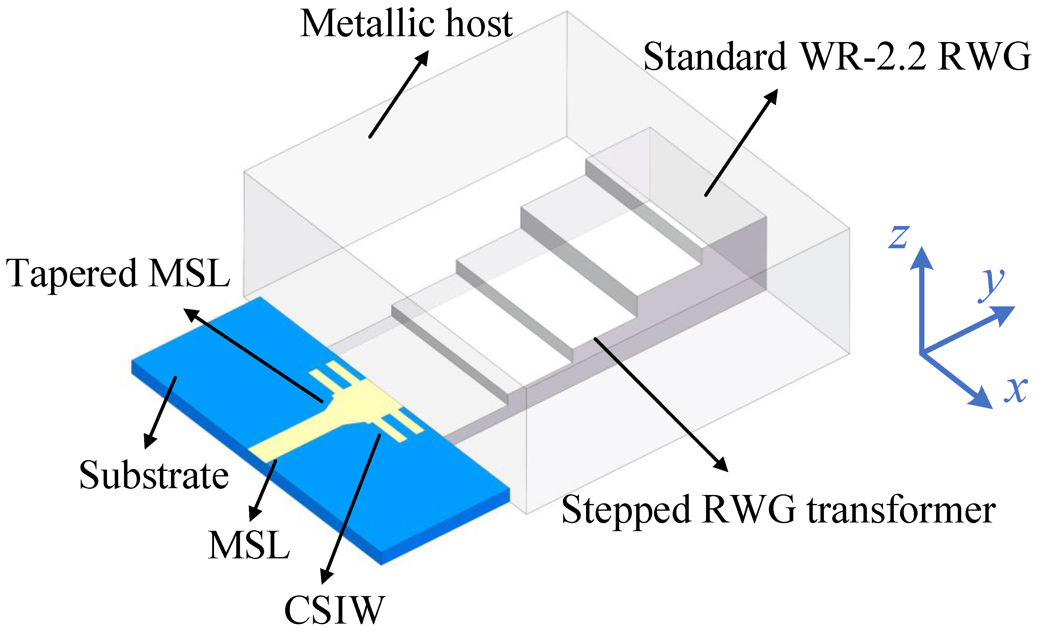
2. Design of the Transition

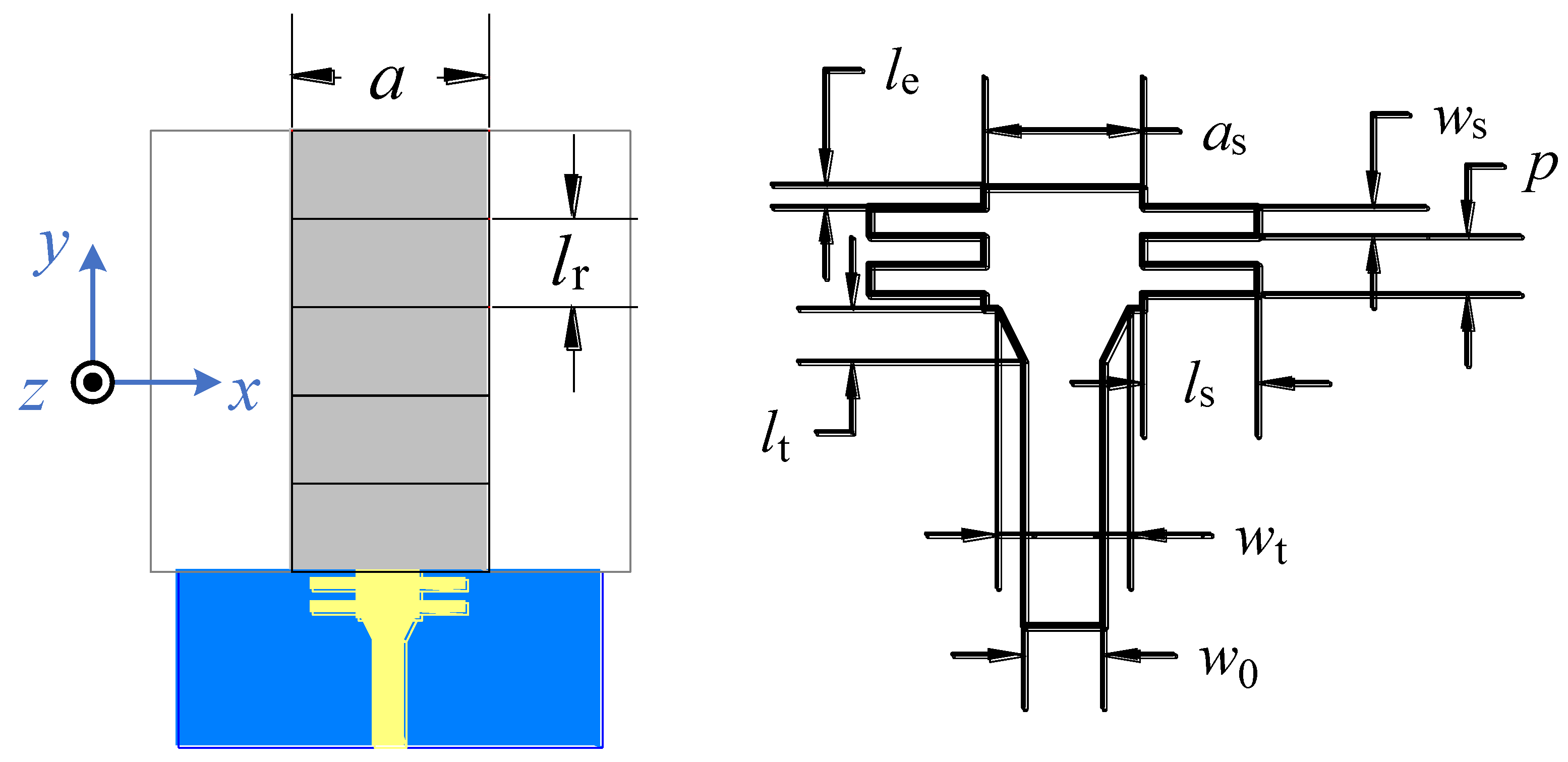
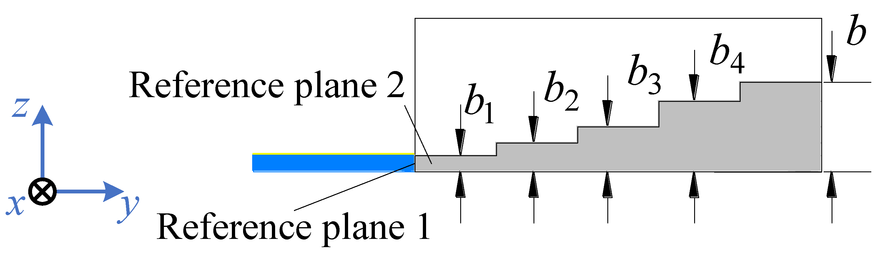
2.1. Transition Model

The proposed MSL-to-RWG transition consists of the substrate section and metallic section, as illustrated in Figure 1. We have used a 50 μm thick quartz substrate (εr = 4.4) for THz operation, and the golden patterns have the thickness of 0.7 μm. The ground plane is on the bottom of the substrate, which is connected to the metallic host. We define the MSL input port as port 1, and the RWG output port as port 2. The input MSL has a width of 0.09 mm (52.2 Ω at 325 GHz), the output port is a standard WR-2.2 RWG with the inner dimension of 0.559 mm × 0.2795 mm.
In the proposed transition, the MSL is first coupled to the CSIW through a tapered MSL on substrate. Second, the CSIW is connected to the standard WR-2.2 RWG through a stepped RWG transformer. Figure 2 shows the vertical view of the proposed MSL-to-RWG transition, and the configuration of the MSL-to-CSIW transition section. Figure 3 shows the side view of the proposed MSL-to-RWG transition, along with a clear definition of the stepped RWG transformer. The detailed dimensions of the proposed transition are summarized in Table 1.

2.2. Working Principles

The CSIW propagates similar to the TE10 mode as the SIW with the same host waveguide width (as). This is different from the SIW, in which via holes are used to create sidewalls, and the CSIW uses open circuit stubs to create PMC sidewalls [17,18]. Considering the on-chip packaging circumstances, where DC bias is needed for active devices, the top and bottom layers of the SIW are naturally grounded due to the existence of via holes, and extra capacitor structures need to be introduced. The CSIW replaces via holes of the SIW by PMC sidewalls, where the top and bottom layers are isolated, and benefits packaging. Leaky-wave antennas based on CSIW have also been proposed because of these unique advantages [19,20].
As mentioned in Section 1, for MSL-to-RWG transitions that use dielectric filled RWGs, perfect electric conductor (PEC) sidewalls are provided by metallic supporting channels of the same widths as RWGs, and the dielectric has to be shaped to fit in the channel. As for the CSIW, PEC sidewalls are replaced by PMC sidewalls, and a shaped dielectric is not required. Based on the above analysis, the CSIW is a better choice for our type of MSL-to-RWG transition than SIW or dielectric filled RWG.
For the MSL-to-CSIW transition section, the electromagnetic wave from the input MSL propagates into the tapered MSL with a width of wt and length of lt, and couples into the CSIW section, as shown in Figure 2. The tapered MSL can be regarded as a transformer between quasi-TEM mode and TE10-like mode, which serves as the feeding structure for the CSIW. In order to achieve a compact structure, the length of the tapered MSL should be as short as possible. The influence of lt on S-parameters is further discussed in Section 2.3.
For verification of the CSIW section, Figure 4 presents the layout of the CSIW and simulated results of the back-to-back structure of the MSL-CSIW transition. Please note that the parameter values in Figure 4 are the same as that in Figure 2, and only more periods of CSIW units are added in Figure 4. The host waveguide width (as) influences the cut-off frequency of the TE10-like mode, and the length of open circuit stubs (ls) is usually quarter wavelength [18]. The width of open circuit stubs (ws) is half of the period of CSIW units (p).
Considering the RWG, the cut-off frequencies of TEmn modes can be calculated by:
f c = 1 2 π μ ε m π a 2 + n π b 2  
where m and n are mode index, μ and ε are the dielectric constant and permeability, respectively, and a and b are the waveguide dimensions. For the CSIW with PMC sidewalls, the cut-off frequency of the TE10-like mode differs from the RWG, and the dimensions obtained from Equation (1) require optimization. The characteristic impedance Z0 of the first section of RWG transformer (a × b1) can be calculated by:
Z 0 = 2 η b 1 a  
where η = μ / ε . The impedance of the CSIW should be equal to Z0 to achieve good impedance matching, so the host waveguide width (as) and the length of open circuit stubs (ls) were further optimized by software. As shown in Figure 4b, S11 < −13 dB and S21 > −2.6 dB are achieved from 325 to 500 GHz for the MSL-CSIW back-to-back transition. In our design, the length of CSIW section is shortened to achieve a compact structure.
After the MSL-to-CSIW transition is done, the CSIW is straightly connected to the RWG transformer. The transformer consists of four sections with the same width, (a), as the standard WR-2.2 RWG, and the same length of 0.25 mm, (lr). The height of the first section (b1) is equal to the substrate thickness to match the CSIW output, and the next three sections gradually match the RWG of low characteristic impedance to the standard RWG of high characteristic impedance.
In order to explain the transition principles more clearly, the reflection coefficients are simulated at different sections, and shown in Figure 5 as the form of a Smith chart. According to Figure 3, Ref. plane 1 is at the end of the CSIW output on substrate, Ref. plane 2 is at the input port of the RWG transformer. In addition, another model without the CSIW section is created, the reflection coefficient at the end of the tapered MSL section is simulated. The normalized impedance of the chart is 54Ω, which is the characteristic impedance of the first section of RWG transformer (0.559 mm × 0.05 mm) at 413 GHz. As shown in Figure 5, the RWG transformer is able to match the impedance between standard RWG and the RWG with the height of 0.05 mm. The tapered MSL can realize impedance matching to a certain extent, the real parts of the normalized impedance are 0.56 at 325 GHz and 0.41 at 500 GHz. However, there are still some differences between the input impedance at Ref. plane 2, which means it will not be well matched if the tapered MSL is straightly connected to the RWG transformer. This could also explain why additional dielectric filled RWGs have been added to tapered MSLs in [13,14]. By introducing the CSIW section, the real parts of normalized impedance are 0.75 at 325 GHz, and 0.48 at 500 GHz in Ref. plane 1, the input impedance increases and becomes closer to that of the RWG transformer, thus, a better impedance matching with the RWG transformer can be achieved in the entire frequency band. It is worth noting that 325 GHz is close to the cut-off frequency of TE10-like mode of the CSIW, and has a greater insertion loss than other frequencies in Figure 4. This could further increase the input impedance of the CSIW near 325 GHz, making it better matched with the RWG transformer.

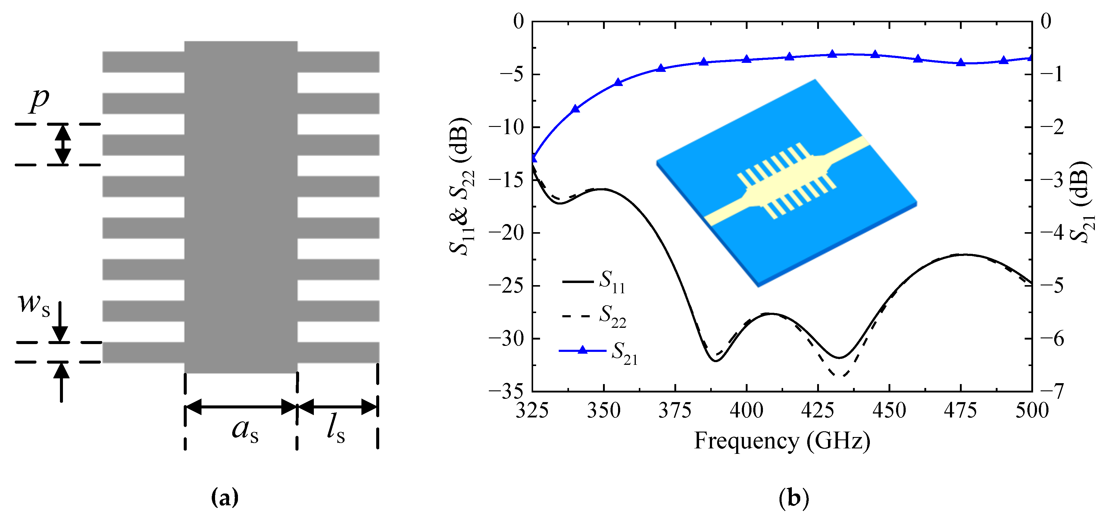
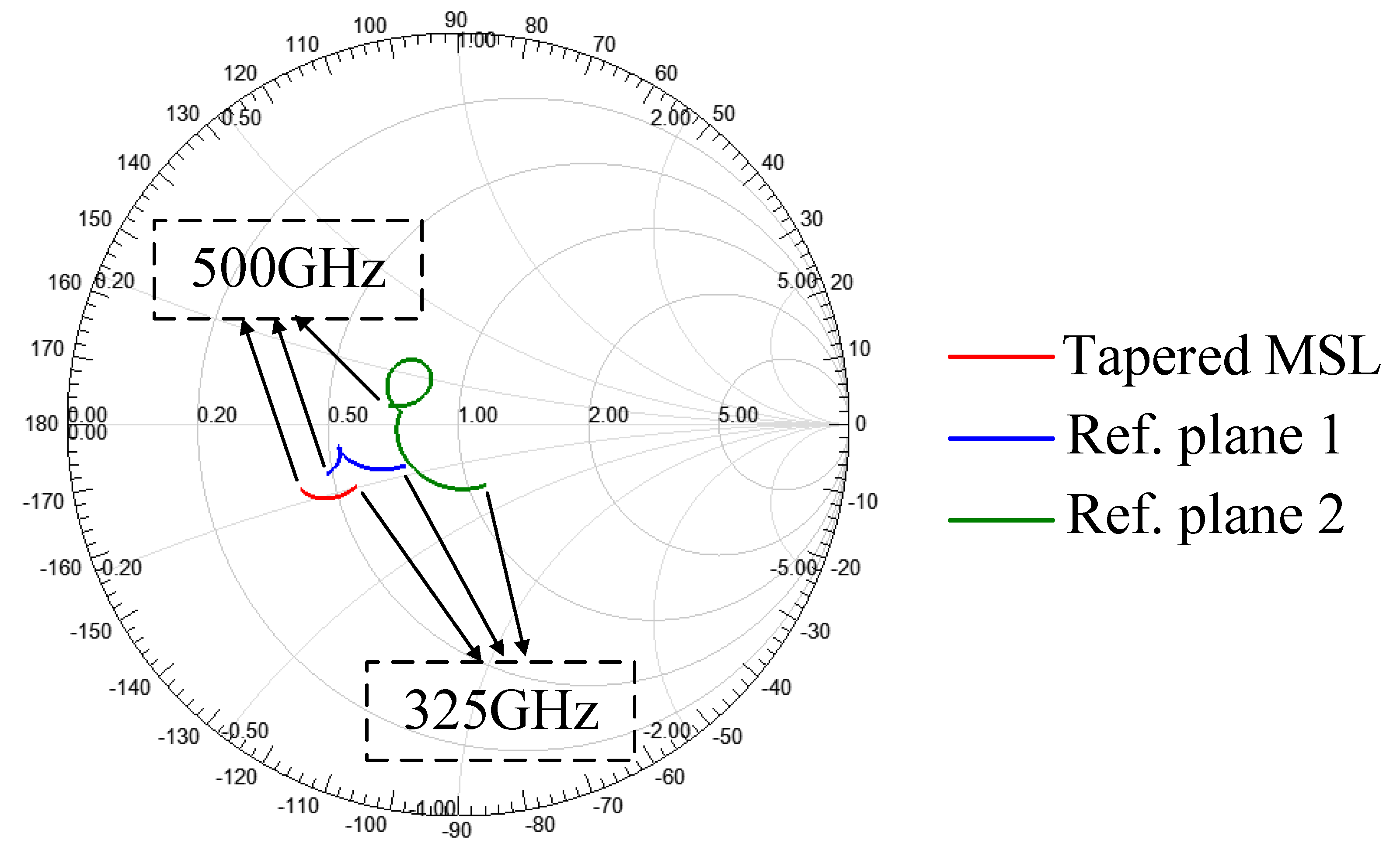
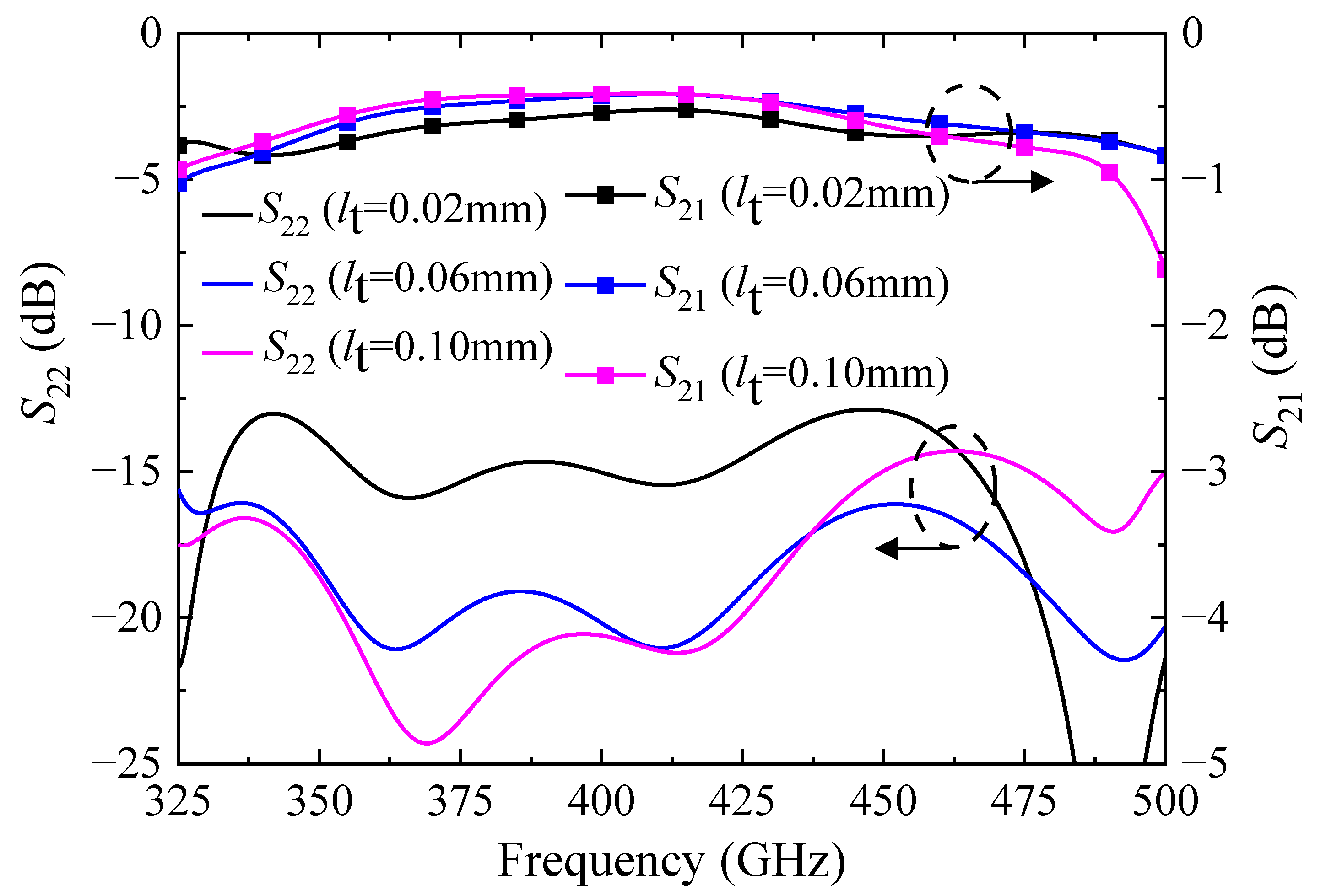
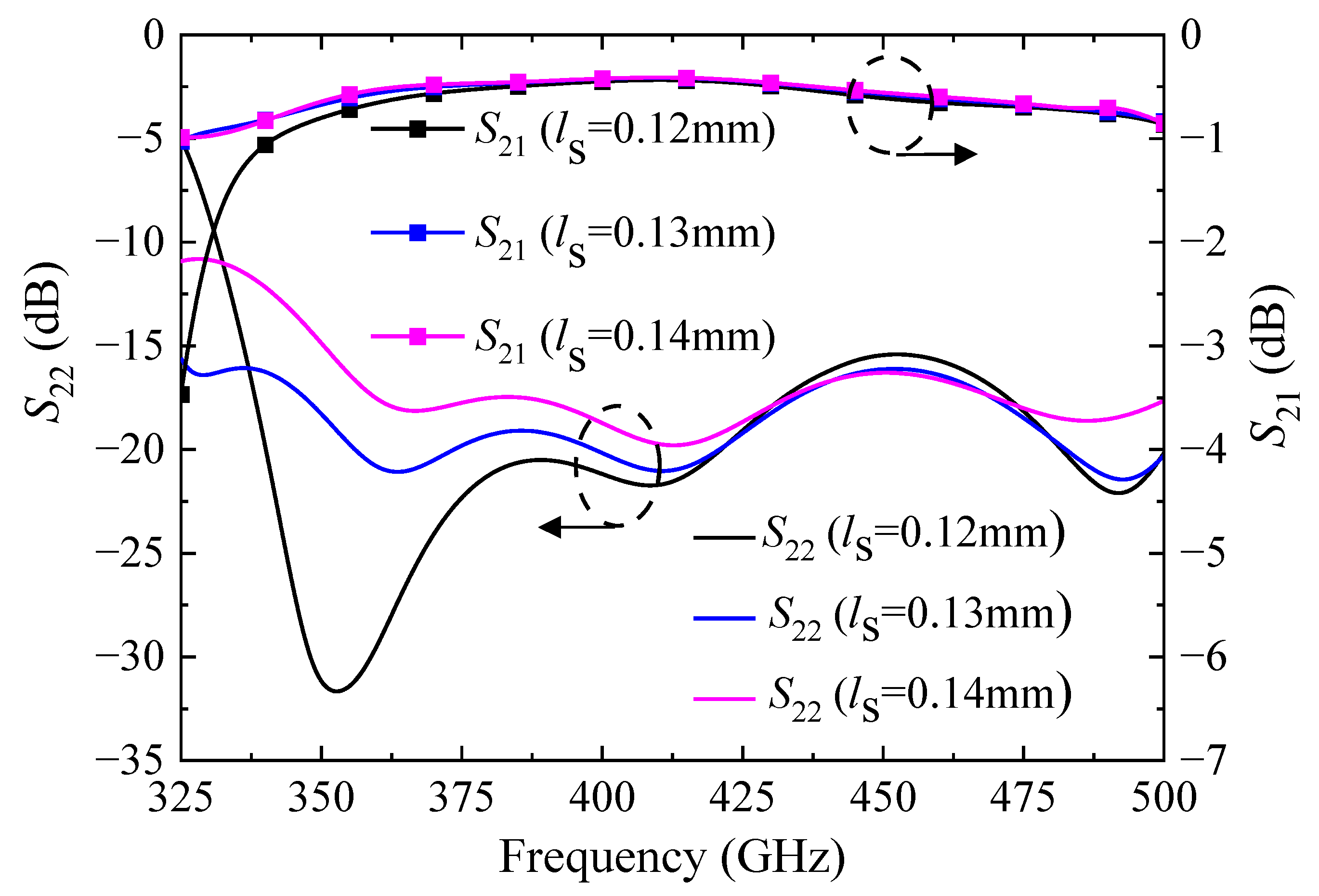
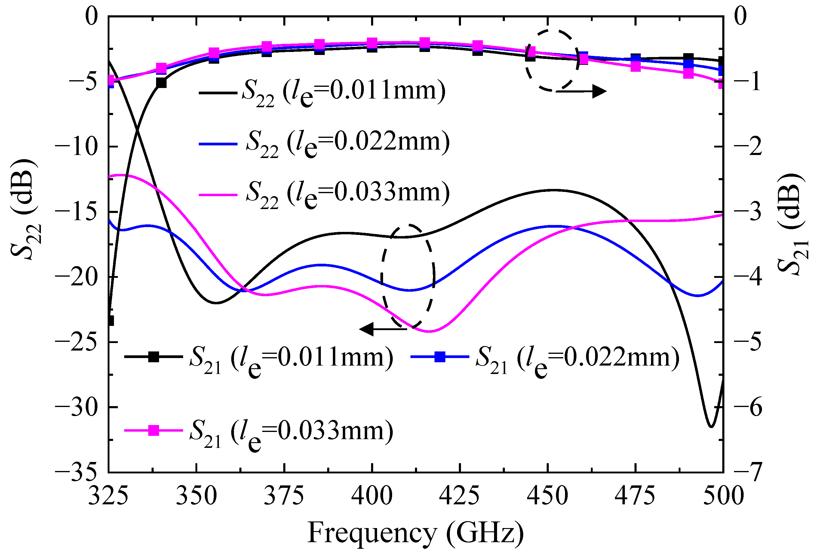
2.3. Parameter Analysis

This Subsection analyzes the influence of some important parameters on S-parameters, which can also be regarded as a reference for designing the proposed transition. The model is given in Figure 1, Figure 2 and Figure 3, we define the MSL port as port 1, and the RWG port as port 2. All parameter values follow Table 1, and when a parameter is being analyzed, all the other parameters remain unchanged. Ansoft HFSS is utilized to give all of the simulation results.
The various lengths of the tapered MSL (lt) are simulated. As presented in Figure 6, the insertion loss is greater at most frequencies when lt = 0.02 mm, and the insertion loss increases near 500 GHz when lt = 0.10 mm. The return loss and insertion loss are both better when lt = 0.06 mm. This illustrates that the length of the tapered MSL cannot be too short.
The host waveguide width (as) of CSIW can be designed according to the desired frequency band, the width of open circuit stubs (ws) and the period of CSIW units (p) are designed according to reference [18]. Afterwards, the length of open circuit stubs (ls) is analyzed. As shown in Figure 7, when ls = 0.12 mm, the PMC sidewall formed by CSIW units is not able to cover the entire band, which results in an insertion loss of 3.5 dB at 325 GHz. When ls ≥ 0.13 mm, the PMC boundary can cover 325–500 GHz. For ls = 0.14 mm, the coupling between open circuit stubs and air-filled RWG becomes more obvious, the S22 becomes slightly worse than ls = 0.13 mm. As a result, ls = 0.13 mm is selected.
Finally, the parameter le is studied. It determines the distance between open circuit stubs and the RWG transformer. As shown in Figure 8, when le = 0.011 mm, the insertion loss at the lower border frequency rises significantly; when le = 0.033 mm, the insertion loss rises at the higher border frequency; and when le = 0.022 mm, the S-parameters are the best from 325 to 500 GHz. When le changes, the period (p) of CSIW units is changed correspondingly, and the operating frequency band of the PMC is shifted. By setting the proper value of le, a broadband transition can be achieved.

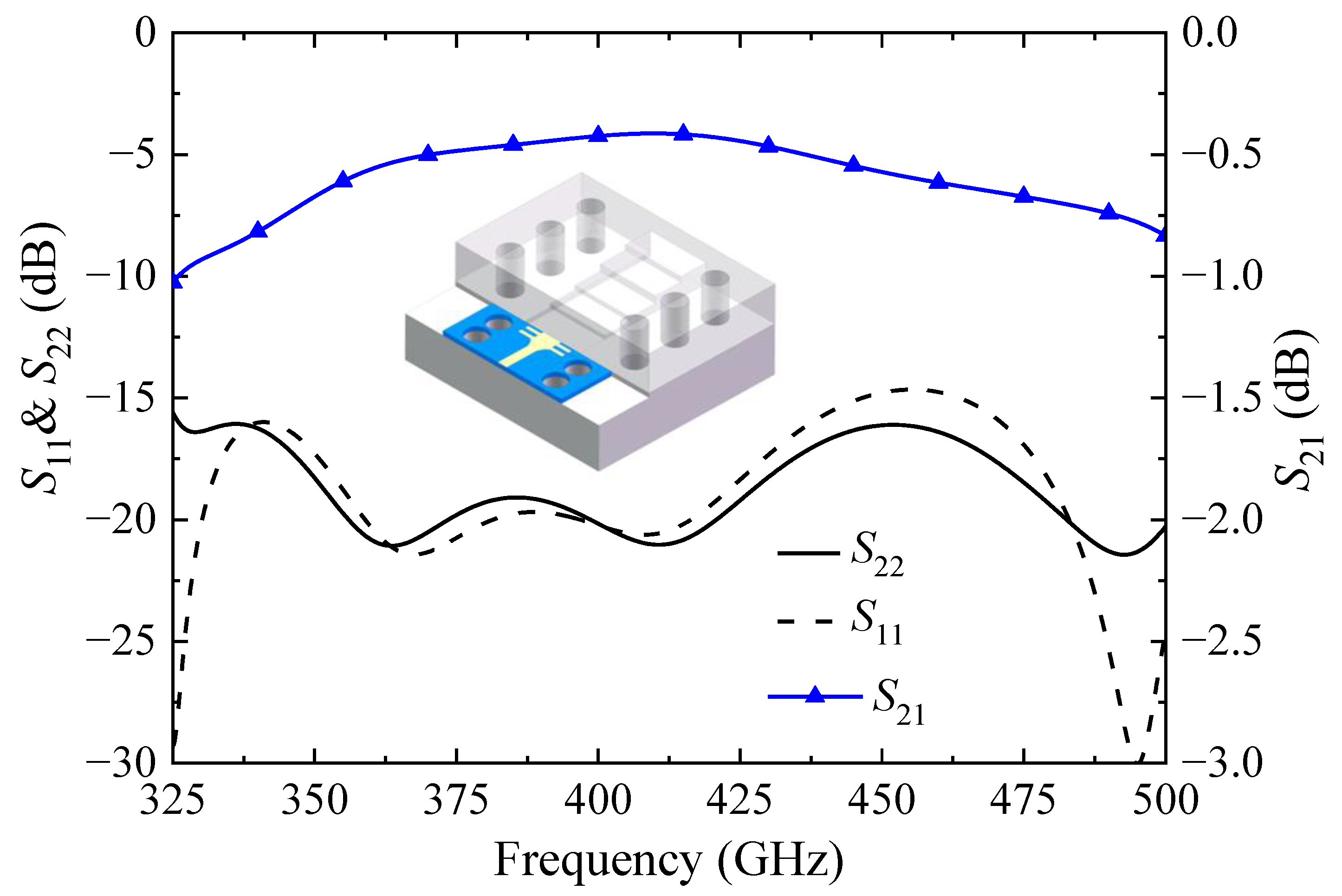
3. Results and Comparisons

3.1. Results

The S-parameters of the proposed MSL-to-RWG transition is given in Figure 9. The structure in Figure 9 has the same inner dimensions as Figure 1, providing a possible method for fabrication, the RWG is split into two blocks and connected by screws, the substrate uses screws to connect to the bottom block. Results of S11 < −14.5 dB, S22 < −15.5 dB, S21 > −1.03 dB are achieved from 325 to 500 GHz. The broadband transition covers the whole frequency band of WR-2.2 RWG with a reasonable insertion loss.

3.2. Comparisons

A comparison between the previously proposed H-plane MSL-to-RWG transitions is summarized in Table 2. Note that all the S-parameters are from simulated results. The reported work focus on microwave and millimeter-wave transitions, while our work focuses on THz applications. Ref. [9] does not require via holes or shaped dielectric, while double side printed circuits are needed which will increase fabrication costs. Refs. [10,11,12] require via holes, and Refs. [12,13,14] require a shaped dielectric. However, in this work, no double side printed circuits, via holes, or shaped dielectric are required, thus, the proposed transition is more applicable in THz bands.

4. Conclusions

In this paper, a compact transition from MSL to RWG is proposed. The transition is realized by two steps, MSL to CSIW transition and CSIW to standard RWG transition. By introducing the CSIW, the impedance matching becomes better, and via holes or a shaped dielectric is not required in this transition. The S11 is better than −14.5 dB and S21 is better than −1.03 dB, and both have been achieved from 325 to 500 GHz. The proposed transition is wideband, compact, and easy to process for THz applications.

Author Contributions

Conceptualization, Z.L. and Y.Y.; methodology, Z.L.; formal analysis, Z.L.; investigation, Q.L.; writing—original draft preparation, Z.L.; writing—review and editing, Y.Y. and X.C. All authors have read and agreed to the published version of the manuscript.

Funding

This work was supported by BUPT Excellent Ph.D. Students Foundation under Grant CX2022118.

Institutional Review Board Statement

Not applicable.

Informed Consent Statement

Not applicable.

Data Availability Statement

Not applicable.

Conflicts of Interest

The authors declare no conflict of interest.

References

  1. Song, H.-J.; Nagatsuma, T. Present and future of terahertz communications. IEEE Trans. Terahertz Sci. Technol. 2011, 1, 256–263. [Google Scholar] [CrossRef]
  2. Leong, Y.-C.; Weinreb, S. Full Band Waveguide-to-Microstrip Probe Transitions. In Proceedings of the 1999 IEEE MTT-S International Microwave Symposium Digest, Anaheim, CA, USA, 13–19 June 1999; Volume 4, pp. 1435–1438. [Google Scholar]
  3. Yao, H.-W.; Abdelmonem, A.; Liang, J.-F.; Zaki, K.A. Analysis and design of microstrip-to-waveguide transitions. IEEE Trans. Microw. Theory Tech. 1994, 42, 2371–2380. [Google Scholar]
  4. Simone, M.; Fanti, A.; Valente, G.; Montisci, G.; Ghiani, R.; Mazzarella, G. A Compact In-Line Waveguide-to-Microstrip Transition in the Q-Band for Radio Astronomy Applications. Electronics 2018, 7, 24. [Google Scholar] [CrossRef] [Green Version]
  5. Deng, B.; Zhang, Q. A wideband MSL-to-WR transition for millimeter wave application. In Proceedings of the 2016 Asia-Pacific International Symposium on Electromagnetic Compatibility (APEMC), Shenzhen, China, 17–21 May 2016. [Google Scholar]
  6. Li, C.L.; Jin, C.; Ma, H.Q.; Shi, X.W. An inline waveguide-to-microstrip transition for wideband millimeter-wave applications. Microw. Opt. Technol. Lett. 2020, 62, 1516–1520. [Google Scholar] [CrossRef]
  7. Zaman, A.U.; Vassilev, V.; Zirath, H.; Rorsman, N. Novel Low-Loss Millimeter-Wave Transition from Waveguide-to-Microstrip Line Suitable for MMIC Integration and Packaging. IEEE Microw. Wirel. Compon. Lett. 2017, 27, 1098–1100. [Google Scholar] [CrossRef] [Green Version]
  8. Belenguer, A.; Ballesteros, J.A.; Fernandez, M.D.; González, H.E.; Boria, V.E. Versatile, Error-Tolerant, and Easy to Manufacture Through-Wire Microstrip-to-ESIW Transition. IEEE Trans. Microw. Theory Tech. 2020, 68, 2243–2250. [Google Scholar] [CrossRef]
  9. Sorocki, J.; Piekarz, I.; Samulak, A.; Delmonte, N.; Silvestri, L.; Marconi, S.; Alaimo, G.; Auricchio, F.; Bozzi, M. Additively Fabricated Air-Filled Waveguide Integrated with Printed Circuit Board Using a Through-Patch Transition. IEEE Microw. Wirel. Compon. Lett. 2021, 31, 1207–1210. [Google Scholar] [CrossRef]
  10. Piekarz, I.; Sorocki, J.; Delmonte, N.; Silvestri, L.; Marconi, S.; Alaimo, G.; Auricchio, F.; Bozzi, M. Wideband Microstrip to 3-D-Printed Air-Filled Waveguide Transition Using a Radiation Probe. IEEE Microw. Wirel. Compon. Lett. 2022, 32, 1179–1182. [Google Scholar] [CrossRef]
  11. Boukari, B.; Moldovan, E.; Affes, S.; Wu, K.; Bosisio, R.G.; Tatu, S.O. Robust Microstrip-to-Waveguide Transitions for Millimeter-Wave Radar Sensor Applications. IEEE Antennas Wireless Propag. Lett. 2009, 8, 759–762. [Google Scholar] [CrossRef]
  12. Hammou, D.; Nedil, M.; Kandil, N.; Moldovan, E.; Tatu, S.O. V-band millimeter-wave microstrip to rectangular waveguide transition. Microw. Opt. Technol. Lett. 2013, 55, 1696–1700. [Google Scholar] [CrossRef]
  13. Zhang, Y.; Ruiz-Cruz, J.A.; Zaki, K.A.; Piloto, A.J. A Waveguide to Microstrip Inline Transition with Very Simple Modular Assembly. IEEE Microw. Wirel. Compon. Lett. 2010, 20, 480–482. [Google Scholar] [CrossRef]
  14. Pérez-Escudero, J.M.; Torres-García, A.E.; Gonzalo, R.; Ederra, I. A Simplified Design Inline Microstrip-to-Waveguide Transition. Electronics 2018, 7, 215. [Google Scholar] [CrossRef] [Green Version]
  15. Cano, J.L.; Mediavilla, A.; Perez, A.R. Full-Band Air-Filled Waveguide-to-Substrate Integrated Waveguide (SIW) Direct Transition. IEEE Microw. Wirel. Compon. Lett. 2015, 25, 79–81. [Google Scholar] [CrossRef]
  16. Moldovan, E.; Bosisio, R.G.; Wu, K. W-band multiport substrate-integrated waveguide circuits. IEEE Trans. Microw. Theory Tech. 2006, 54, 625–632. [Google Scholar] [CrossRef]
  17. Chen, D.G.; Eccleston, K.W. Substrate integrated waveguide with corrugated wall. In Proceedings of the 2008 Asia-Pacific Microwave Conference, Hong Kong, China, 16–20 December 2008. [Google Scholar]
  18. Eccleston, K.W. Mode Analysis of the Corrugated Substrate Integrated Waveguide. IEEE Trans. Microw. Theory Tech. 2012, 60, 3004–3012. [Google Scholar] [CrossRef]
  19. Chen, K.; Zhang, Y.H.; He, S.Y.; Chen, H.T.; Zhu, G.Q. An Electronically Controlled Leaky-Wave Antenna Based on Corrugated SIW Structure with Fixed-Frequency Beam Scanning. IEEE Antennas Wireless Propag. Lett. 2019, 18, 551–555. [Google Scholar] [CrossRef]
  20. Lin, Y.; Zhang, Y.; Liu, H.; Zhang, Y.; Forsberg, E.; He, S. A Simple High-Gain Millimeter-Wave Leaky-Wave Slot Antenna Based on a Bent Corrugated SIW. IEEE Access 2020, 8, 91999–92006. [Google Scholar] [CrossRef]
Figure 1. Three-dimensional view of the proposed MSL-to-RWG transition.
Electronics 12 00614 g001
Figure 2. Vertical view of the proposed MSL-to-RWG transition, with the metallic strip area zoomed in.
Electronics 12 00614 g002
Figure 3. Side view of the proposed MSL-to-RWG transition, and the definitions of two reference planes, named Ref. plane 1 and Ref. plane 2, respectively.
Electronics 12 00614 g003
Figure 4. (a) Layout of the CSIW; (b) Simulated results of the CSIW fed by MSL.
Electronics 12 00614 g004
Figure 5. Smith chart of the reflection coefficients from 325 to 500 GHz at the tapered MSL section, at Ref. plane 1 and Ref. plane 2.
Electronics 12 00614 g005
Figure 6. Simulated S-parameters of the proposed transition with different lt (Solid lines represent S22; lines with square symbols represent S21).
Electronics 12 00614 g006
Figure 7. Simulated S-parameters of the proposed transition with different ls (Solid lines represent S22; lines with square symbols represent S21).
Electronics 12 00614 g007
Figure 8. Simulated S-parameters of the proposed transition with different le (Solid lines represent S22; lines with square symbols represent S21).
Electronics 12 00614 g008
Figure 9. S-parameters of the proposed MSL-to-RWG transition.
Electronics 12 00614 g009
Table 1. Dimensions of the proposed MSL-to-RWG transition (unit: mm).
ParameterValue
a0.559
as0.18
w00.09
wt0.15
ws0.033
lt0.06
ls0.13
le0.022
lr0.25
p0.066
b0.2795
b10.05
b20.09
b30.14
b40.22
Table 2. Comparisons between different H-plane MSL-to-RWG transitions.
Ref.Frequency (GHz)S11 (dB)S21 (dB)Requirement of Via Holes/Shaped Dielectric
[9]18–24<−15About −0.86No
[10]8.2–12.4<−10About −0.18Yes
[11]74–79<−10-Yes
[12]60–64<−10>−1.5Yes
[13]8.2–10<−10>−1.5Yes
[14]75–110<−10>−1Yes
This work325–500<−14.5>−1.03No
Disclaimer/Publisher’s Note: The statements, opinions and data contained in all publications are solely those of the individual author(s) and contributor(s) and not of MDPI and/or the editor(s). MDPI and/or the editor(s) disclaim responsibility for any injury to people or property resulting from any ideas, methods, instructions or products referred to in the content.

