1. Introduction
The low noise amplifier (LNA) is one of the important components in the front end of the radar receiver, and its noise figure directly affects the sensitivity of the receiver. At the same time, it is hoped that it has a wider bandwidth to capture a wider range of signals; higher gain flatness within the operating bandwidth will ensure the dynamic range of the receiver is not degraded. Small size and low power consumption are the constant pursuit of radar receivers, especially for phased array radars.
From the design point of view, these parameters all affect each other. For example, the input standing wave ratio and noise are contradictory, because when matching the input impedance of the transistor, the minimum noise impedance and the optimal standing wave impedance are conjugates of each other. At the same time, increasing the current can reduce the noise, because the minimum noise of a transistor is inversely proportional to the trans-conductance, and the trans-conductance is proportional to the drain current. The power consumption and linearity are also contradictory. Therefore, to obtain better indicators for each parameter, many attempts have been made, and various LNA architectures have been designed.
The cascode amplifier can provide relatively flat gain and noise in broadband [
1], but usually the gain is not high. It can be increased by increasing the number of stages, but the noise will also deteriorate [
2]. Ref. [
3], which is based on complementary metal oxide semiconductor (CMOS) technology, adopts the structure of resistive shunt-shunt feedback, and realizes the gain of 17 dB and the noise of 3 dB under the single-stage cascode structure by adding an L-type passive matching. Ref. [
4] adds an inductor at the source stage of the common source amplifier to achieve simultaneous noise and impedance matching. Ref. [
5] adopts noise canceling common gate LNA structure, using inductively degenerated common source stage in parallel with common gate stage instead of common source stage. The current reuse [
6,
7] architecture is widely used in CMOS circuits, especially in the case of low power consumption. Ref. [
8] uses noise cancellation and current reuse techniques to design a 3.19 GHz~8.8 GHz LNA. Ref. [
9] is based on current reuse technique and adopts shunt-shunt resistive feedback and degenerative parallel inductance and capacitance (LC) technique to achieve high gain and low noise factor for a 3.1 GHz~10.6 GHz wideband LNA.
However, based on III-V compound technology, few articles have been reported on LNA using current reuse architecture. For broadband LNAs, most literatures adopt common-source (CS) or cascode structures. Ref. [
10] designs an X-band LNA based on the GaAs process using a three-stage CS structure. Ref. [
11], based on GaN-on-SiC technology, designs a medium-power LNA in which the first two stages adopt current reuse architecture and the final stage adopt a CS structure.
The current reuse architecture can provide higher gain while ensuring lower noise, and is small in size and low in power consumption. It is a structure suitable for receiver front-end amplifier. However, the conventional structure cannot obtain enough bandwidth. In this paper, the current reuse architecture is improved to expand the bandwidth. Moreover, the front end of the receiver is usually affected by the environment because it is close to the external antenna end, and the tape-out process will also drift, resulting in a large change in the performance of the amplifier. This paper designs an LNA that is less affected by temperature and process for the front end of the receiver, and whose state is still adjustable after tape-out.
2. Principle Design
2.1. Current Reuse Architecture
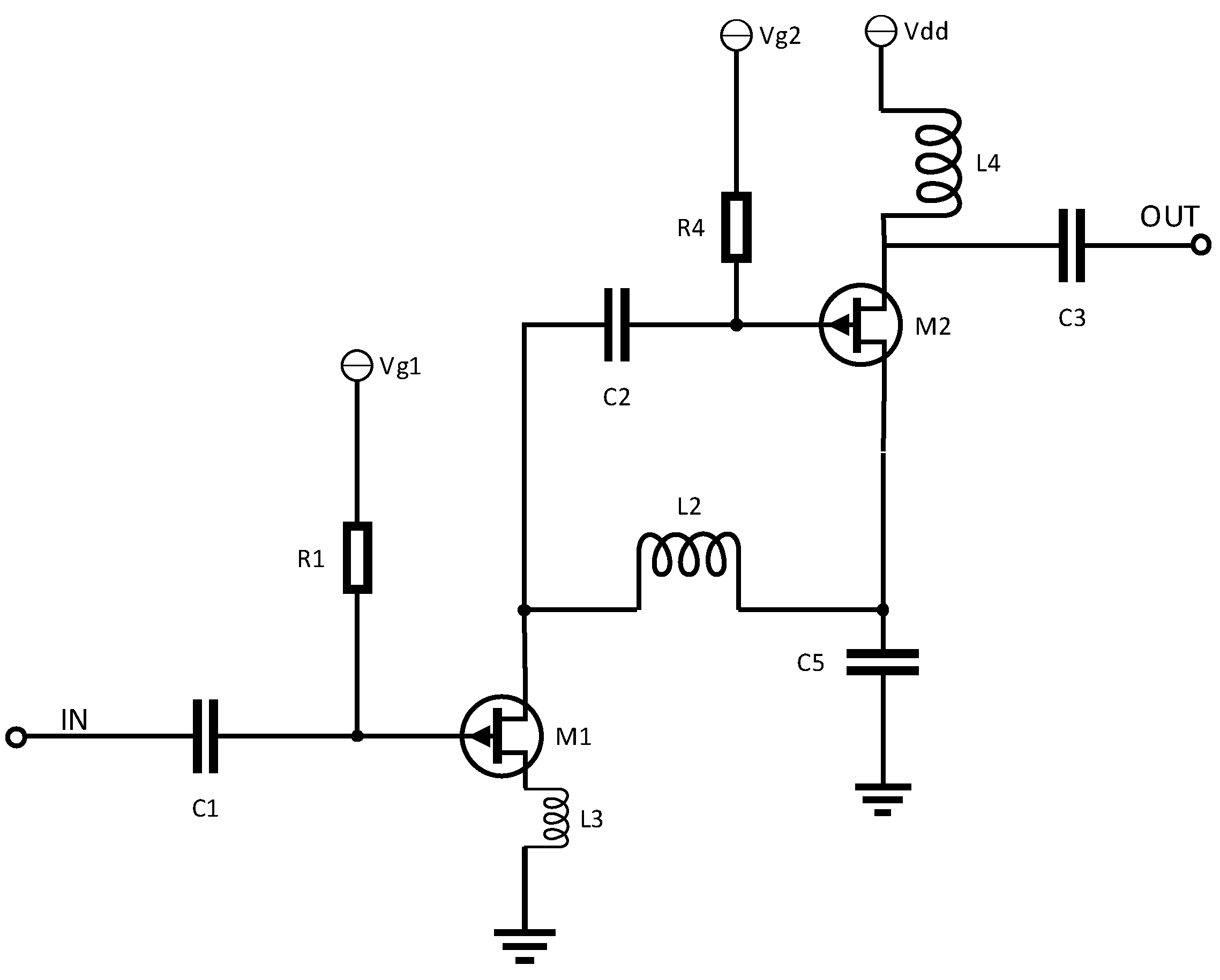
Figure 1 shows the schematic of a current reuse LNA. On the direct current (DC) path, M1 and M2 are connected in series and share current. The power supply voltage drain drain (VDD) powers the drain of M2 through a choke inductor L4. M2 is turned on at a certain gate voltage VG2. The current flows through the source of M2 to the drain of M1 through a choke inductor L2, and M1 is turned on at a certain gate voltage VG1. The source of M1 is connected in series with the inductor L3 to improve the stability of the amplifier.
The current reuse architecture can be regarded as two-cascaded CS amplifiers which share the same amount of current. The input radio frequency (RF) signal is first amplified by M1, coupled to the gate of M2 via capacitor C2, and output after being amplified by M2 in the second stage. C5 provides RF ground for M2.
The first-stage common-source amplifier is analyzed. Usually, the alternating current (AC) input impedance of the transistor is relatively low, and the gate needs to be connected in series with a resistance for input impedance matching, but this increases noise power and degrades efficiency. Adding an inductance in series with the source of the transistor can create a resistive input impedance without adding noise resistors, which is called inductive source degeneration.
Figure 2a is the basic AC circuit using the inductor
placed in series with the source of the device, and
Figure 2b is a simplified model of its equivalent circuit, where
(the gate-drain parasitic capacitance),
(the drain-source parasitic capacitance) and
(the drain-source conductive channel resistance) are ignored here.
For an input current I at the gate of the transistor, the
(the gate-source parasitic capacitance) voltage
, the transistor’s gate-to-ground voltage is shown in Equation (1):
where
Ri represents the input resistance of the undepleted part of the gate under channel,
represents the transconductance. The input impedance looking into the gate is shown in Equation (2):
From the input impedance, it can be concluded that to obtain a 50 Ω input impedance at the operating frequency, appropriate values of
and
need to be selected so that
is resonated at the operating frequency, and
needs to be set equal to 50 Ω.
So the series inductor can be chosen to match the input resistance of the amplifier to 50, and the inductor can be chosen to cancel the residual input reactance, which is usually capacitive.
2.2. Adaptive Bias Circuit
In order to reduce the influence of temperature, process fluctuation and voltage change, a current mirror plus source-negative feedback bias circuit is designed. The basic schematic diagram is shown in
Figure 3. Resistor R1 and transistor M1 form an input stage to convert current into voltage, By adjusting gate-source voltage
, drain current
. Here the gate of M1 is connected to the drain, forming a diode-like connection, which can be equivalent to a resistor. M2 is the output stage, which converts voltage into current, its gate is used as voltage input, and its drain is used as current output. When the channel length modulation effect is ignored and the influence of the process is ignored, it is considered that the mobility μ of the transistor and the deviation of the unit gate oxide capacitance
Cox can be ignored. Then the circuit can accurately replicate the current regardless of process and temperature variations, and its output current is only related to the ratio of the transistor size, i.e.,
, so as to stabilize the working state of the amplifier.
3. Circuit Design
3.1. Process Selection
The GaAs pseudomorphic high electron mobility transistor (pHEMT) process has two types: E-mode and D-mode. In order to obtain even lower noise, analyze the influence of different processes on noise, the high-frequency noise figure of the transistor can be obtained from the transistor equivalent circuit and can be expressed as Equation (3) [
12]:
where
represents the white noise of the transistor. It can be seen that the higher the cut-off frequency of the transistor, the smaller the noise of the transistor itself; and the higher the frequency of the transistor, the bigger the noise figure.
If the influence of parasitic inductance and resistance is ignored, the cut-off frequency of the transistor depends on
and
, can be expressed as Equation (4) [
13]:
The typical peak
value of 0.15 μm E-mode pHEMT process is about twice that of 0.15 μm D-mode pHEMT process, however, for a transistor of the same size, the difference of the drain capacitance and source capacitance between these two processes is negligible. The cut-off frequency of 0.15 μm E-mode pHEMT process is about 1.2 times that of D-mode process [
14].
Thus the E-mode process with higher transistor cut-off frequency is adopted for this design.
3.2. Circuit Design
3.2.1. Circuit Topology
Designed using PE15 process of Win Semiconductors,
Figure 4 is the schematic of the proposed X-band LNA.
From the cut-off frequency Formula (4), it can be seen that large trans-conductance or small inter-electrode capacitance can yield a high cut-off frequency, which is contradictory, because a large-size transistor has higher trans-conductance, but also larger inter-electrode capacitance, so there should be trade-off between the gate width and parallel gate fingers during the design to obtain better noise figures.
After careful comparative analysis, both stages use a 4 × 50 um transistor. As
Figure 4 show, L1 and L2 provide DC paths, R1, R2, C4, and L1 form the feedback loop. Among them, M3~M6 and M1 form a current mirror. In order to reduce the influence of channel-length modulation, by connecting M3, M4, M5, and M6 in series, the gate is short-circuited, which is equivalent to increasing L. W remains unchanged, which is equivalent to a transistor of W/4L. The longer the channel, the higher the drain voltage, and the higher the replication accuracy.
The current of the entire amplifier depends mainly on the first-stage, and an on-chip voltage divider is used to adjust the first-stage gate voltage, thereby through controlling the bias current of the first-stage transistor, the current of the amplifier is controlled.
The specific current trimming function is achieved by reserving four pads on the chip and bonding the pads to either the power supply or ground to adjust the ratio of the potential divider.
The bias circuit helps to resist the variation of the quiescent operating point caused by process and temperature variation. A resistor of about 1 kΩ is connected in series between the bias circuit and the gate of the first stage transistor to reduce the noise caused by the bias circuit. Meanwhile, an extra pad is reserved for the gate of the second stage transistor, and the operating point of the transistor can be adjusted by externally providing the gate voltage, which can be used as a debugging method.
3.2.2. Matching Design
First select the intermediate frequency point and find the optimal source and load impedance. In the design process, it is necessary to find out the best noise matching impedance and the best power matching impedance, draw the circular diagram as shown in
Figure 5, and find the balance point of the two in the circular diagram. As shown in
Figure 5, the impedance is about 63 + j50, and then the impedance matching design is carried out.
3.2.3. Gain Design
As the gain of the microwave transistor decreases with frequency [
15], so the gain in the entire frequency band will show a negative slope trend. To obtain the best noise and gain matching over the entire frequency band, the matching parameters need to be adjusted, some measures can be taken to improve the gain at the high frequency end.
- (1)
Influence of feedback inductance
L1, C4, and R2 form the feedback circuit of the first-stage amplifier, which is used to widen the frequency band. The easier the frequency band passed by the feedback circuit, the smaller the output power. Therefore, the in-band flatness can be optimized by adjusting the feedback. For example, the inductance of the front stage L1 can be increased. At this time, the LC resonance frequency decreases, and the input voltage standing wave ratio (VSWR) will move to the low end, as shown in
Figure 6.
- (2)
Architecture improvements
In addition, the traditional current reuse architecture is improved. A small capacitor is connected to the ground in parallel with the drain of the first-stage transistor. The capacitor acts as a channel for high frequency, so the high frequency part is less fed back, which can suppress high-frequency feedback, thereby improving the high-frequency output gain and expanding the bandwidth.
It can be seen from
Figure 6 that before the improvement (without C6), the gain of the traditional architecture starts to decrease after the frequency reaches 10 GHz, and the gain decreases by about 3 dB when the frequency reaches 12 GHz. After the improvement (with C6), under the new architecture the gain decreases very little when the high frequency band reaches 12 GHz, and the frequency band is successfully extended to 12 GHz.
- (3)
Influence of inter-stage capacitance
There are other influencing factors, such as increasing the inter-stage capacitance, and the noise can also be reduced. However, the VSWR becomes worse, as shown in
Figure 7; In addition, the source stage grounding wire can be shortened, but the VSWR becomes worse also.
- (4)
Influence of source resistance
The source of the first stage amplifier is connected to the negative feedback circuit to the ground, and the small-signal model is analyzed as shown in
Figure 8. When there is no source resistor, calculate the voltage gain:
where
with source resistors, calculate the voltage gain:
When the small-signal trans-conductance changes due to the change of the mobility μ of the transistor and the capacitance of the unit gate oxide, the state of the amplifier will change, and this change is relatively small due to the influence of source resistor (), and the larger the value of , the smaller the state change of the amplifier.
As shown in
Figure 9, it is assumed here that the conduction parameter
, composed of μ and
, deviates by about 20%. It can be seen that when Rs increases, the gain of the amplifier becomes smaller, but the operating point of the amplifier is more stable, and the change of the amplifier gain with process and temperature is smaller.
3.2.4. Stability Design
The source of the first stage transistor is connected with a micro-strip line as a degeneration inductor to improve the stability of the amplifier, which also benefits the input match. The effect of adding this series micro-strip on the stability factor is simulated and calculated, as
Figure 10 shows. After adding a micro-strip, the stability factor K is greater than 1, and |Δ|is less than 1, according to Rollet’s condition [
16], the amplifier is unconditional stability.
3.2.5. Final Layout
All performance parameters affect each other [
17]. The trend is that the more slope of the gain, the better the VSWR. It is necessary to consider all parameters in a balanced manner and find the optimal combination. The photograph is shown in
Figure 11.
4. Experimental Results
4.1. Test Methods and Results
The S-parameters measurement is carried out on a probe platform with a calibrated vector network analyzer. When the bias adjusting pads are left open, by default the chip is biased with 5 V 30 mA at room temperature. The input power of the VNA is set to −20 dBm, which guarantees enough SNR while keeping the output power within the linear region of the VNA receiver. Measured data (dotted lines) and simulation results (solid lines) show good conformance. As shown in
Figure 12, the input return loss is less than −10 dB, and the output return loss is less than −17 dB within the entire operation frequency range. The measured gain is about 24.4 dB with excellent flatness, and can well extend its operation frequency down to 6 GHz.
Figure 13 shows the measured stability factor curve.
Because the VNA the probe platform equipped has no noise measurement option, the die is assembled onto a test fixture shown in
Figure 14, then the noise figure is measured with a dedicated noise analyzer. Finally, the insertion loss of the input RF connector and the micro-strip line is de-embedded as shown in
Figure 15, the noise figure is less than 0.8 dB within the entire frequency range, and is as low as 0.65 dB@6 GHz. It also shows that the output 1 dB gain compression point is between 14 dBm and 15.6 dBm at room temperature, which is fair enough for a LNA biased with only 30 mA.
Figure 16 shows the measured two-tone test curve, and the OIP3 of the LNA can be calculated to be 26.56 dBm.
The feasibility of the proposed LNA is commonly entrenched using a pertinent figure of merit (FoM) that calibrate its accomplishment. The FoM is included with band-width (BW), gain, output power at 1 dB compression point, noise temperature (noise figure), power consumption, and area to meet wide-band low power system target given as Equation (8) [
18,
19]:
The larger the value, the better the overall performance.
Table 1 encapsulates the measured performance of the proposed LNA and compares it with advanced LNAs that have similar frequency bands. It is clear from
Table 1 that the higher values of FoM of the proposed LNA prove better in comparison with other LNAs.
4.2. Gain Adjustment Effect
Four pads are reserved on the chip as shown in
Figure 11, and the operating point of the chip can be adjusted by bonding these reserved pads to VDD or GrouND (GND), and then the gain and current of the chip can be adjusted. This adjustment method can be achieved through a simple gold wire. Bonding is performed on-chip, and no additional power supply is required.
When the reserved pads are all floating, the typical current is 30 mA. When VG1C is bonded to the VDD pad, the current will increase by 8 mA. At this time, the gain will increase by 1.5 dB, and the P1dB will increase by 1.5 dB; when VG1D is bonded to the VDD pad, the current will increase by 3.5 mA. At this time, the gain is increased by 0.9 dB, and the P1dB is increased by 0.7 dB; when VG1A is bonded to the GND pad, the current will decrease by 4 mA. At this time, the gain will be decreased by 1.0 dB, and the P1dB will be decreased by 1.0 dB; when VG1B is bonded to the GND pad, the current will decrease by 8.5 mA. At this time, the gain will be decreased by 1.8 dB, and the P1dB is reduced by 2.6 dB. The above adjustments have little effect on noise and standing waves.
In addition, the chip also reserves a gate voltage control pad VG2. The VDD voltage divide ratio across the current reuse architecture can be adjusted by applying a voltage to pad VG2 from an external power supply.
Table 2 takes the frequency point 10 GHz as an example to show the effect of the gain adjustment by different bonding scheme, of course, more gain states can also be obtained through different combinations of bonding schemes.
In addition, thanks to the structure of current reuse, the two-stage amplifiers are connected in series on DC, dividing VDD to the two-stage transistors. The amplifier supports a wider power supply voltage range, which can support +4 V to +6.5 V. When the power supply changes, the amplifier state is shown in the
Table 3 below.
4.3. Temperature Effect
Usually, the performance of a chip changes greatly with temperature. Thanks to the active bias circuit, the gain variation is only about 1.5 dB and the current drift is only about 3 mA within the operating temperature range of −40 °C to +85 °C, as shown in
Figure 17.
Table 4 gives an overview of the chip performance.
5. Conclusions
An 8 GHz~12 GHz LNA is implemented based on current reuse architecture with PE15 process. It features ultra-low noise figure, high gain and extremely low power consumption, which is suitable for radar receiver front-end. This design has three innovations:
Firstly, the current reuse architecture is improved in this paper. By connecting a small capacitor in parallel with the drain of the first-stage transistor, the function of expanding the frequency band is achieved and the flatness of the X-band LNA is improved.
Secondly, an innovative bias circuit is designed based on GaAs process. The first point is to improve the accuracy of current replication by short-circuiting the gates of multiple transistors, which is equivalent to increasing the gate length. The second point is to improve the linearity under large signal by adding an RC circuit in the bias circuit.
Thirdly, a design method for on-chip state adjustment is proposed. Through different pad-bonding combinations the gain adjustment range of the chip is greater than 3 dB, the OP1dB adjustment range is greater than 4 dB, and the current adjustment range is greater than 16 mA.


 ,
, 


