1. Introduction
Recently, Transformer [
1] has been widely used in NLP tasks and provides a tremendous performance improvement over the traditional Convolutional Neural Network (CNN) and Recurrent Neural Network (RNN) models. By avoiding the recurrent calculations and taking full advantage of the attention mechanism, the Transformer has achieved state-of-the-art accuracy in various NLP tasks. However, attention runs terribly slow on general-purpose platforms such as GPUs and CPUs. Therefore, designing efficient hardware accelerators for the Transformer is of great necessity. With high parallelism and low latency, FPGA is widely used for hardware acceleration. The most resource-intensive modules in Transformer, including MHA and FFN blocks, can be well implemented in hardware through systolic array architecture [
2,
3].
Systolic arrays are also widely seen in various accelerator designs such as [
4,
5,
6,
7,
8,
9]. By reusing input data multiple times, it enables high operational throughput with less bandwidth consumption. The systolic array architecture has high parallelism and is suitable for hardware acceleration on FPGA. However, many systolic array designs suffer a low frequency of FPGA implementation. This paper aims to tackle this problem and provide a Transformer accelerator with a high-frequency runtime configurable systolic array on FPGA. The key contributions of this work are as follows:
A high-frequency systolic array design with variable functionality and much less resource usage that can switch between tasks such as MHA and FFN by dynamically changing the functionality of DSP slices.
The regularity of the systolic array can be finely preserved at implementation, while each cell of the systolic array is undertaken by only one DSP slice on the FPGA device.
A semi-automatic design flow for high-frequency systolic arrays on FPGA is proposed as a general solution, together with an automated XDC (Xilinx Design Constraints) constraint file generator to preserve the regularity of large systolic arrays on different FPGA devices.
The remainder of this paper is organized as follows. The backgrounds of the Transformer and the systolic array are presented in
Section 2. The method of deploying a systolic array with conserved topology and fine-tuned DSP configuration is shown in
Section 3. We then describe the proposed design flow in
Section 4.
Section 5 presents the model architecture and crucial blocks of the Transformer, and
Section 6 shows the accelerator architecture. We provide the experimental result in
Section 7. Finally, the paper is concluded in
Section 8.
2. Background
In this section, we focus on the background and recent works in terms of the model architecture of the Transformer and the systolic array.
2.1. The Model Architecture of the Transformer
Transformer [
1] is well known for its superior performance in the natural language processing (NLP) area. The Transformer contains an encoder stack and a decoder stack, and all the encoder layers and the decoder layers are composed of two kinds of ResBlocks, i.e., the Multi-Head Attention (MHA) ResBlock and the position-wise Feed-Forward Network (FFN) ResBlock. An MHA ResBlock consists of
h Attention Heads, while each Attention Head composes of three linear layers and a Scaled Dot-Product Attention function that follows. The parameter
h is equal to 8 in the Transformer base model or equal to 16 in the Transformer big model. The input of each Attention Head includes three tensors:
V (values),
K (keys), and
Q (queries), which is the same as the input of the MHA ResBlock.
Vi,
Ki, and
Qi are generated from the three linear layers in each Attention Head, shown in Equation (1):
while the Scaled Dot-Product Attention function in the MHA ResBlock is described in Equation (2):
The mask operation masks out all values of illegal connections before the softmax. The parameter
dk is equal to 64 in both the Transformer base model as well as the Transformer big model. The FFN ResBlock contains a layer normalization [
10] operation, residual addition, a ReLU activation, and two linear sublayers, described in Equation (3):
The massive amount of matrix computations and complicated data flow make it necessary to design efficient hardware architectures for the Transformer. Reference [
2] proposes a hardware accelerator for the Transformer with a reconfigurable hardware architecture based on a systolic array for the MHA ResBlock and the FFN ResBlock. However, in this design, the systolic array has not been optimized for FPGA deployment. Reference [
11] provides a Transformer neural network inference accelerator with Set-Associative Rearranged Compressed Sparse Column Format to enable large-scale MACs (Multiply and Accumulate) to maintain high utilization. Pruning in Transformers has been researched in depth in recent works for the purpose of reducing data storage and computational requirement: Reference [
12] accommodates Transformer onto FPGA with Vivado High-Level Synthesis (HLS), using a block-balanced pruning technique and their proposed special storage format, while Reference [
13] presents an efficient transformer-based large-scale language representation using hardware-friendly block structure pruning, and Reference [
14] provides a novel structural pruning method with memory footprint awareness and designs the associated accelerator on FPGA. Due to the high complexity of the Transformer, many hardware accelerator designs choose the Vivado High-Level Synthesis tool for development. As an automatic process, High-Level Synthesis accepts synthesizable code written in high-level languages (such as C, SystemC, and C++) and transforms them into an RTL design. Reference [
15] develops a customized hardware accelerator for the Transformer using Vivado HLS and performs different optimization for different data types. Reference [
16] designs a customized hardware accelerator for the Transformer by using Vivado HLS. Reference [
17] develops a framework that builds inference accelerators on FPGA platforms for quantized Vision Transformers with binary weights and low-precision activations and uses the Vivado HLS for hardware implementations. Reference [
18] proposes an energy-efficient acceleration framework for transformer-based large-scale language representations, and also uses the Vivado HLS tool for the synthesis step.
Although HLS is often adopted for its convenience in the design of hardware, it is worth noting that using a behavioral approach rather than a structural approach to describe hardware may lead to a lack of preciseness of design intention. To avoid this obvious drawback, we chose to use a better hardware design approach. As a kind of hardware generation language (HGL), the SpinalHDL [
19] language raises the level of abstraction from RTL description to RTL generation and utilizes a high-level language named Scala for describing the generation intent. SpinalHDL achieves its high design productivity by providing object-oriented programming, functional programming, and meta-hardware description that enables parametrization and Verilog code generation. Therefore, in this work, we choose to use the SpinalHDL language for Transformer hardware design to increase the level of abstraction while retaining RTL-level granularity.
2.2. The Systolic Array
The architecture of the systolic array is capable of tackling the timing issue for massive parallelization while delivering high performance for a wide range of applications. Therefore, it will be competent for crucial matrix operations in Transformer hardware acceleration. The systolic array runs in a regular and synchronized manner to perform fine-grained pipelining between neighboring data processing units (called cells). At every clock cycle, each cell reads inputs from its neighbors (above or on the left), performs computation, and passes forwards the inputs and results to other neighbors (below or on the right). By such means, high computational throughput is realized, and bandwidth consumption is reduced, for the input data are reused constantly. The feature of local interconnect minimizes long datapaths to meet the target clock frequency. Furthermore, various algorithms can be implemented by reusing the same systolic array structure but with different computation cell logics, which exhibits the broad applicability of systolic array architecture. Output stationary and weight stationary are the two well-known dataflows for computational tasks such as matrix multiplication, according to [
8,
9]. For instance, a typical systolic array acceleration takes in input feature maps and weight and returns results during the calculation of matrix multiplication. Weight stationary dataflow indicates that the weight is preloaded into cell buffers and remains stationary inside them while executing calculation. Output stationary dataflow suggests that the input feature maps and weight flow through the systolic array while the result remains stationary in the cells during calculation. In this work, we adopt the output stationary dataflow.
Reference [
2] proposes a hardware accelerator for the Transformer with systolic array architecture. However, this design only uses the traditional RTL-based design methodology, which does not make full use of the DSP resources of the FPGA, so there is a relatively large room for frequency enhancement. Reference [
4] implements CNN on an FPGA with systolic array architecture, which can achieve high clock frequency as well as increased resource utilization. Reference [
8] use Chisel language to build hardware module templates for systolic architecture, and the templates can be reused for different dataflows and computation algorithms. SuSy [
20] introduces a compilation flow that enables high-performance systolic arrays building with productivity on FPGAs, as well as a programming framework composed of a domain-specific language (DSL). AutoSA [
21] also provides an end-to-end compilation framework for generating high-performance systolic arrays on FPGA. The works in SuSy and AutoSA have good performance in terms of frequency, reaching 250 MHz and 300 MHz, respectively. We hope to achieve a better performance of higher frequency in this work.
3. Deployment of Systolic Array with Conserved Topology and Fine-Tuned DSP Configuration on FPGA
In the systolic array, each cell is identical, forming a shape of a regular 2D mesh, which can bring simple and regular data and control flow to hardware implementation, avoiding high fan-out, thus being friendly for place and route. Although systolic arrays have a layout-friendly topology, existing FPGA EDA tools cannot synthesize and place them on FPGA with high quality. According to [
22], the limitation of the EDA tool will lead to structure distortion of systolic arrays in the actual layout, causing many implementations of systolic arrays on FPGAs to suffer a lower frequency than expected. Additionally, the EDA tool may not fully exploit the capability of DSP resources, should a finely designed configuration not be given.
Therefore, in this design, we manually deploy the designed circuit logic onto the DSPs by means of instantiating the DSP macro IP (intellectual property) and configuring them at compile-time and runtime, pushing the utilization of each DSP slice to a higher level. We also leverage the generator methodology and the object-oriented feature of SpinalHDL to generate Verilog HDL code for DSP configuration and instantiation in batches, which can maximize efficiency while retaining the maximum precision for configuring the DSP’s functional and timing paths. In addition, the size of the proposed systolic array can be adjusted freely to explore optimal designs on FPGA devices with different resources through our design flow.
DSPs are high-speed arithmetic resources on FPGA. The DSP48E2 slice on Xilinx Ultrascale devices consists of a 27-bit pre-adder, 27 × 18 multiplier, and a flexible 48-bit ALU (arithmetic logic unit) that serves as a post-adder/subtracter, accumulator, or logic unit, which is capable of performing various calculational tasks. Considering that the functional ability of a single DSP slice is powerful enough and its configurability is remarkably high, we adopt a mapping method of one cell corresponding to one DSP slice. Every DSP slice accepts direct input signals including A (30 bits), B (18 bits), C (48 bits), and D (27 bits), and cascaded input signals ACIN (30 bits), BCIN (18 bits), and PCIN (48 bits). We take full advantage of the dedicated cascaded channels between the DSP slices in the same column on board, for they do not consume additional routing resources, which is beneficial to optimizing the routing effect and increasing the frequency. Since cascaded channels can only be used along columns, we can only use additional routing resources for the datapaths vertical to the DSP columns. More details will be discussed in
Section 6.
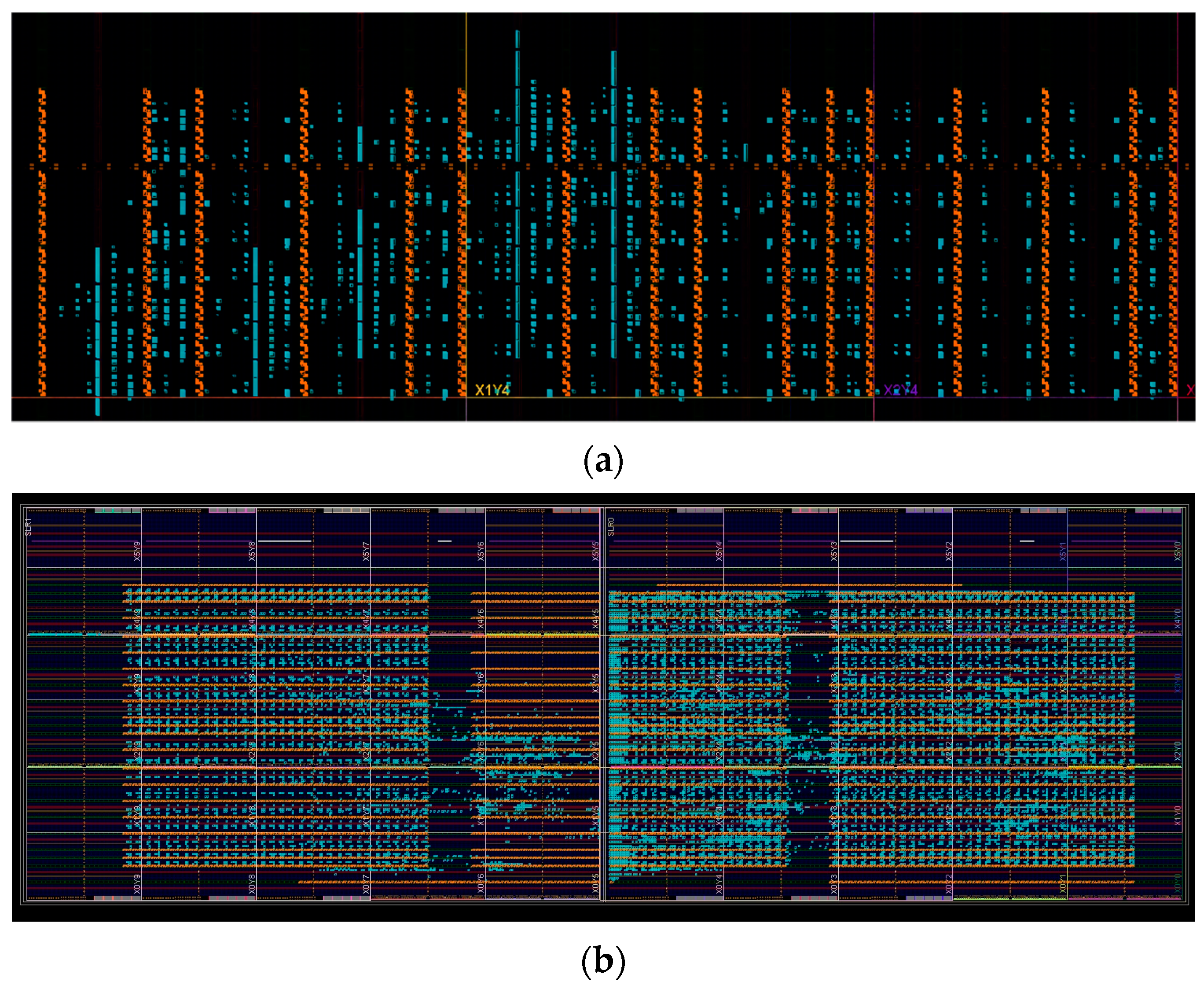
The constraint-generating tool we design that can automatically generate XDC constraints will take the size of the target systolic array and the resource arrangement of different FPGA devices as input, then adjust the overall layout structure of the systolic array and restrict cells to fixed locations while ensuring its homogeneity and leveraging the DSP column resources as much as possible. It can be seen that in
Figure 1, DSP slices of the systolic array (marked in orange) are finely arranged with the help of the constraint-generating tool, and the regularity of their layout is preserved to the maximum. For small size systolic array, it will be directly arranged as a regular mesh like that in
Figure 1a. However, when the side length of the systolic array exceeds the number of DSP columns, the proposed tool will compromise appropriately and adjust accordingly for optimal results such as those in
Figure 1b. With such a regular topology of placement, we manage to achieve high frequency for both small- and large-scale systolic arrays.
To summarize, the fine-tuned DSP configuration has three important features. Firstly, we adopt a mapping method of one cell corresponding to one DSP slice, and by compile-time and runtime configurations, the DSP resources are fully leveraged. Secondly, datapaths between cells are, therefore, datapaths between DSP slices, and we can take full advantage of the dedicated cascaded channels along DSP columns to save routing resources and increase the frequency. Lastly, we lay out all of the DSP slices with the XDC placement constraint file generated by scripts in order to preserve the regularity of the layout of the systolic array in deployment.
4. Proposed Design Flow
Considering the versatility of the systolic array design and the common frequency issue that occurred when deployed on FPGAs, we hope to propose a more general solution. A semi-automatic design flow for high-frequency systolic arrays for FPGA deployment is designed and implemented, which is shown in
Figure 2.
The design flow has three main entrances that start from the main design written in SpinalHDL, marked by serial numbers (①–③) in the diagram according to the sequence of the actual steps in the design flow. Starting from entrance ①, we first perform cell design and dataflow design that should be verified as DUT1 (design under test) in comparison with the software golden model in functional simulation 1. After several modifications, DUT1 that passed the functional simulation 1 will become the hardware golden model. Secondly, starting from entrance ②, we map the design on DSP slices by means of fine configuration and instantiation, which should pass the verification as DUT2 in functional simulation 2 in comparison with the software golden model and hardware golden model. The well-configured DSP slices, as DUT2, should exhibit the exact same functionality as DUT1, so as to pass the functional simulation 2. Starting from entrance ③, XDC files are generated automatically and sent to the FPGA physical design tools for placement constraints together with the synthesized design. Using the timing reports analysis as feedback, we continue to iterate the design loop until the optimal design is found. Such design flow is also beneficial to implementing systolic arrays of different sizes onto FPGA devices with different resource budgets.
5. Model Architecture and Crucial Blocks of Transformer
The standard Transformer contains an encoder and a decoder, consisting of three kinds of blocks, i.e., the Multi-Head Attention (MHA) ResBlock, the Feed-Forward Network (FFN) ResBlock, and the Residual Addition and Layer Normalization block; the MHA and the FFN ResBlocks have the highest numbers of FLOPs and occupy most of the storage space, according to Reference [
23]. In this work, we mainly focus on these key modules in Transformer for accelerator design. The specific computational tasks as well as the module used for these tasks are presented in detail in
Table 1. For the steps containing tasks such as matrix multiplication, matrix addition, matrix transposition, and ReLU activation function, the same proposed systolic array is used for their calculation. The steps containing softmax and layer normalization are performed in the Softmax module and LayerNorm module, respectively. The design of the Softmax module is partially based on the design of Reference [
24].
6. Accelerator Architecture
The overall architecture of our accelerator is shown in
Figure 3. The system architecture mainly includes Host, external memory DRAM (dynamic random access memory), on-chip buffer, accelerator in programmable logic, and on-chip and off-chip bus interconnection. The accelerator receives data from external memory DRAM through an AXI connection with the help of DMA (direct memory access). The data reorder module rearranges the data as needed and passes them to multiple buffers. The read/write arbiter module controls read and write between multiple buffers and the systolic array. The systolic array receives data input from both the left and top directions while performing calculation tasks, and the result can be output from one of the two directions after the calculation is completed (for matrix transposition purposes). The size of the systolic array is configurable at compile time and is denoted as
SA_size. We set up six buffers in the accelerator for Weight, Bias, X, Q, K, and V, respectively. Each buffer consists of
SA_size RAMs (random access memory), while each RAM has a depth of
Buffer_Depth, and its data width is 8 bits. Therefore, at each clock cycle, data with the number of
SA_size are fetched by the fetch logic from one buffer and sent to the corresponding
SA_size ports of the systolic array in the left or top direction. Two of the buffers are selected each time to provide the corresponding data for the systolic array, and they are controlled by the main control module. A multiple clock domains design is adopted, considering that the frequency of the Softmax module and the LayerNorm module is generally lower than that of the systolic array. Asynchronous FIFOs (First In First Out) are used when the data are passed between the fast clock domain and slow clock domain.
6.1. MHA Task
Matrix multiplication and matrix addition are the most significant tasks in the Multi-Head Attention block. When performing matrix multiplication and matrix addition (present in
Figure 4a,b), at every cycle, each cell applies the same MAC (Multiply and Accumulate) operation to its inputs from left and above and then passes the computed result and its unmodified inputs to its adjacent cells, such that there is minimal data movement and high computational concurrency. Each row or column accepts data one cycle earlier than the row below it or the column next to its right side. For matrix addition mode in
Figure 4b, an input matrix of 0s with 1s on the diagonal is used on one side, while the bias matrix to be added is on the other side.
According to the proposed design flow, we design circuit logic for each cell, map the design on DSP slices with primitive level configuration, and instantiate the configured DSP slices in batches. As mentioned in
Section 3, every DSP slice accepts four direct input data signals, including A, B, C, D, and three cascaded input data signals, ACIN, BCIN, and PCIN, shown in
Figure 5b. Considering that cascaded channels can only be used along columns, we use BCIN-BCOUT channels for B signal input and PCIN-PCOUT channels for P signal output. For the datapaths vertical to the DSP columns, i.e., signal A entering the systolic array and the P signal outputting from it, we can only use additional routing resources, shown in
Figure 5a.
For MAC tasks, the DSP configuration and their functionalities are set as follows (the datapaths for different purposes are marked in different colors for distinction in
Figure 5a): inside each DSP slice, after receiving the A signal (direct input, marked in blue) and the BCIN signal (cascade input, marked in red), a multiplication operation is first performed on them, and the operation result is sent to the ALU through MReg (register named M, marked in orange). Then, the calculation result of the ALU is forwarded to the PReg (register named P) for registration. The result of PReg is sent back to the other input end of the ALU through a loop (marked in cyan), then accumulated with the data passed from MReg in the next clock cycle. After calculation, the result of all cells can be output from one of the two directions (left or down, marked in green), shown in
Figure 5a.
Figure 5b shows the configuration of DSP48E2 in detail. The valid datapaths are colored in the same way as shown in
Figure 5a, and they are matched accordingly.
6.2. FFN Task
In the FFN task, the main computational procedures involve matrix multiplication, matrix addition, and Rectified Linear Unit (ReLU) activation function. We map the ReLU activation function into each DSP slice of the systolic array for greater efficiency and higher DSP utilization. By such means, the FFN task can also be fully implemented on the proposed systolic array. The ReLU activation function is shown in Equation (4):
As shown in
Figure 5b, in order to determine the positivity or negativity of the calculation results, we perform sign bit recognition on the most significant bit of the calculation result of the ALU by using pattern recognition through configuring the signals MASK and PATTERN of DSP slices. Only calculation results that are greater than 0 will be allowed to be output; otherwise, they will be substituted by 0. By implementing the ReLU function inside the DSP slice, we manage to conserve LUT (lookup table) resources to a greater extent.
6.3. Matrix Transposition Task
The matrix transpose operation is an indispensable part of the attention mechanism. The matrix transposition task in the MHA requires a transposition of the result of the calculation. We propose an efficient method to realize such transposition in two steps. Firstly, after the calculation, the result can be output from the systolic array in two perpendicular directions, left or below. Secondly, the result can be written into the buffer in two directions by controlling the write address order, i.e., from the most significant address to the least significant address or the opposite. By changing the output direction and the write address order at the same time, the matrix transposition is realized, as shown in
Figure 4c. With such a design, no additional transpose unit is required.
7. Experimental Result
We mainly compare our results with previous systolic array accelerators on FPGA to prove the effectiveness of our frequency optimization. Our design is evaluated on Xilinx ZCU102 (with a similar chip process to related designs) for different array sizes by using the Vivado 2021.2. With the help of the proposed design flow and fine-tuned configuration, the maximum frequency of our design is much higher than related designs and achieves 588 MHz and 474 MHz for different sizes, which is 1.8× and 1.5× improvement compared to the best recent design [
8], demonstrated in
Table 2. Since we did not find the exact same array sizes as our design for comparison in recent designs, we chose the designs with similar dimensions for comparison. A similar dimension implies similar parallelism and therefore leads to meaningful comparisons. Based on our refined DSP configurations method, we manage to fully leverage DSP resources and save them drastically by 84% compared to Reference [
21] with similar systolic array dimensions. By the mapping method of one cell corresponding to one DSP slice and the refined configuration of DSP slices, we manage to save a tremendous amount of DSP resources and enable an exact correspondence between the amount of DSP utilization and the size of the systolic array. At the same time, by placing a large number of calculation processes inside the DSP, the usage of FlipFlop and LUT can also be significantly reduced, as shown in
Table 3.
8. Conclusions
In this work, we present a Transformer accelerator based on a well-designed high-frequency systolic array for FPGA deployment, achieving a frequency improvement of up to 1.8× while significantly reducing DSP, FlipFlop, and LUT resource usage. In terms of innovation, the proposed systolic array can realize the calculations of both MHA and FFN blocks through runtime configuration on DSP slices, while fully leveraging the DSP resources. Furthermore, the systolic array based on refined DSP configurations, the design flow as a general solution, and the placement constraint-generating tools proposed in this paper are of universal reference values for more similar designs intending to implement a higher-frequency systolic array on FPGA.
Admittedly, one of the limitations of this work is that we only focus on key modules in Transformer for accelerator design. More effort is spent on the systolic array part of the accelerator.
In future work, we plan to upgrade the Transformer accelerator with more complete and comprehensive functionalities. Additionally, based on the proposed design flow, we envision a fully automatic design flow as a universal solution for FPGA-based high-frequency systolic array deployment.
Author Contributions
Conceptualization, Y.C. and T.L.; methodology, Y.C. and T.L.; validation, Y.C.; investigation, Y.C. and X.C.; resources, T.S.; data curation, Y.C. and X.C.; writing—original draft preparation, Y.C.; writing—review and editing, T.L. and T.S.; supervision, T.S.; project administration, Y.C. and T.S.; funding acquisition, T.S. and Z.C. All authors have read and agreed to the published version of the manuscript.
Funding
This research was funded by the Key-Area Research and Development Program of Guangdong Province, China (Grant No. 2020B0404030003); and the Science and Technology Planning Project of Guangdong Province, China (Grant No. 2021B1212050003).
Data Availability Statement
The data presented in this study are available on request from the corresponding author. The data are not publicly available due to privacy.
Conflicts of Interest
The authors declare no conflict of interest.
References
- Vaswani, A.; Shazeer, N.; Parmar, N.; Uszkoreit, J.; Jones, L.; Gomez, A.; Kaiser, Ł.; Polosukhin, I. Attention Is All You Need. In Advances in Neural Information Processing Systems; Curran Associates, Inc.: Red Hook, NY, USA, 2017; Volume 30, Available online: https://proceedings.neurips.cc/paper/2017/hash/3f5ee243547dee91fbd053c1c4a845aa-Abstract.html (accessed on 31 January 2023).
- Li, S.; Wang, M.; Liang, S.; Lin, J.; Wang, Z. Hardware Accelerator for Multi-Head Attention and Position-Wise Feed-Forward in the Transformer. In Proceedings of the 2020 IEEE 33rd International System-on-Chip Conference (SOCC), Las Vegas, NV, USA, 8–11 September 2020; pp. 84–89. [Google Scholar] [CrossRef]
- Ye, W.; Zhou, X.; Zhou, J.T.; Chen, C.; Li, K. Accelerating Attention Mechanism on FPGAs Based on Efficient Reconfigurable Systolic Array. ACM Trans. Embed. Comput. Syst. 2022. [Google Scholar] [CrossRef]
- Automated Systolic Array Architecture Synthesis for High Throughput CNN Inference on FPGAs | Proceedings of the 54th Annual Design Automation Conference 2017. Available online: https://dl.acm.org/doi/abs/10.1145/3061639.3062207 (accessed on 28 November 2022).
- Chen, Y.-H.; Krishna, T.; Emer, J.S.; Eyeriss, V.S. Eyeriss: An Energy-Efficient Reconfigurable Accelerator for Deep Convolutional Neural Networks. IEEE J. Solid-State Circuits 2017, 52, 127–138. [Google Scholar] [CrossRef]
- Das, S.; Roy, A.; Chandrasekharan, K.K.; Deshwal, A.; Lee, S. A Systolic Dataflow Based Accelerator for CNNs. In Proceedings of the 2020 IEEE International Symposium on Circuits and Systems (ISCAS), Seville, Spain, 12–14 October 2020; pp. 1–5. [Google Scholar] [CrossRef]
- Zeng, Y.; Sun, H.; Katto, J.; Fan, Y. Accelerating Convolutional Neural Network Inference Based on a Reconfigurable Sliced Systolic Array. In Proceedings of the 2021 IEEE International Symposium on Circuits and Systems (ISCAS), Daegu, Republic of Korea, 22–28 May 2021; pp. 1–5. [Google Scholar]
- Jia, L.; Lu, L.; Wei, X.; Liang, Y. Generating Systolic Array Accelerators With Reusable Blocks. IEEE Micro 2020, 40, 85–92. [Google Scholar] [CrossRef]
- Genc, H.; Haj-Ali, A.; Iyer, V.; Amid, A.; Mao, H.; Wright, J.; Schmidt, C.; Zhao, J.; Ou, A.; Banister, M.; et al. Gemmini: An agile systolic array generator enabling systematic evaluations of deep-learning architectures. arXiv 2019, arXiv:1911.09925. [Google Scholar]
- Lei, J.; Kiros, J.R.; Hinton, G.E. Layer Normalization. arXiv 2016, arXiv:1607.06450. [Google Scholar]
- Park, J.; Yoon, H.; Ahn, D.; Choi, J.; Kim, J.-J. OPTIMUS: OPTImized Matrix MUltiplication Structure for Transformer Neural Network Accelerator. Proc. Mach. Learn. Syst. 2020, 2, 363–378. [Google Scholar]
- Accommodating Transformer onto FPGA | Proceedings of the 2021 on Great Lakes Symposium on VLSI. Available online: https://dl.acm.org/doi/abs/10.1145/3453688.3461739 (accessed on 29 December 2022).
- Li, B.; Kong, Z.; Zhang, T.; Li, J.; Li, Z.; Liu, H.; Ding, C. Efficient Transformer-Based Large Scale Language Representations Using Hardware-Friendly Block Structured Pruning. arXiv 2020, arXiv:2009.08065. [Google Scholar]
- Zhang, X.; Wu, Y.; Zhou, P.; Tang, X.; Hu, J. Algorithm-Hardware Co-Design of Attention Mechanism on FPGA Devices. ACM Trans. Embed. Comput. Syst. 2021, 20, 71:1–71:24. [Google Scholar] [CrossRef]
- Peng, H.; Huang, S.; Geng, T.; Li, A.; Jiang, W.; Liu, H.; Wang, S.; Ding, C. Accelerating Transformer-Based Deep Learning Models on FPGAs Using Column Balanced Block Pruning. In Proceedings of the 2021 22nd International Symposium on Quality Electronic Design (ISQED), Santa Clara, CA, USA, 7–9 April 2021; pp. 142–148. [Google Scholar] [CrossRef]
- Bahmani, M. Accelerating Transformer Deep Learning Models on FPGAs Using High-Level Synthesis. Laurea, Politecnico di Torino. 2021. Available online: https://webthesis.biblio.polito.it/17894/ (accessed on 31 January 2023).
- Sun, M.; Ma, H.; Kang, G.; Jiang, Y.; Chen, T.; Ma, X.; Wang, Z.; Wang, Y. VAQF: Fully Automatic Software-Hardware Co-Design Framework for Low-Bit Vision Transformer. arXiv 2022, arXiv:2201.06618. [Google Scholar]
- FTRANS | Proceedings of the ACM/IEEE International Symposium on Low Power Electronics and Design. Available online: https://dl.acm.org/doi/abs/10.1145/3370748.3406567 (accessed on 1 February 2023).
- Papon, C. SpinalHDL. 2021. Available online: https://github.com/SpinalHDL/SpinalHDL (accessed on 31 January 2023).
- Lai, Y.-H.; Rong, H.; Zheng, S.; Zhang, W.; Cui, X.; Jia, Y.; Wang, J.; Sullivan, B.; Zhang, Z.; Liang, Y.; et al. SuSy: A Programming Model for Productive Construction of High-Performance Systolic Arrays on FPGAs. In Proceedings of the 2020 IEEE/ACM International Conference on Computer Aided Design (ICCAD), Virtual Event, USA, 2–5 November 2020; pp. 1–9. [Google Scholar]
- AutoSA | The 2021 ACM/SIGDA International Symposium on Field-Programmable Gate Arrays. Available online: https://dl.acm.org/doi/abs/10.1145/3431920.3439292 (accessed on 28 November 2022).
- Zhang, J.; Zhang, W.; Luo, G.; Wei, X.; Liang, Y.; Cong, J. Frequency Improvement of Systolic Array-Based CNNs on FPGAs. In Proceedings of the 2019 IEEE International Symposium on Circuits and Systems (ISCAS), Sapporo, Japan, 26–29 May 2019; pp. 1–4. [Google Scholar] [CrossRef]
- Ganesh, P.; Chen, Y.; Lou, X.; Khan, M.A.; Yang, Y.; Sajjad, H.; Nakov, P.; Chen, D.; Winslett, M. Compressing Large-Scale Transformer-Based Models: A Case Study on BERT. Trans. Assoc. Comput. Linguist. 2021, 9, 1061–1080. [Google Scholar] [CrossRef]
- Wang, M.; Lu, S.; Zhu, D.; Lin, J.; Wang, Z. A High-Speed and Low-Complexity Architecture for Softmax Function in Deep Learning. In Proceedings of the 2018 IEEE Asia Pacific Conference on Circuits and Systems (APCCAS), Chengdu, China, 26–30 October 2018; pp. 223–226. [Google Scholar] [CrossRef]
| Disclaimer/Publisher’s Note: The statements, opinions and data contained in all publications are solely those of the individual author(s) and contributor(s) and not of MDPI and/or the editor(s). MDPI and/or the editor(s) disclaim responsibility for any injury to people or property resulting from any ideas, methods, instructions or products referred to in the content. |
© 2023 by the authors. Licensee MDPI, Basel, Switzerland. This article is an open access article distributed under the terms and conditions of the Creative Commons Attribution (CC BY) license (https://creativecommons.org/licenses/by/4.0/).


