1. Introduction
The recent advances in transistors and Metal-Insulator-Semiconductor (MIS) structures have allowed the development of Metal Oxide Semiconductor Field Effect Transistors (MOSFETs), Thin Film Transistors (TFTs), and Dynamic Random-Access Memories (DRAMs). High-performance electronic devices require thin film oxides with high quality and dielectric constant to achieve high capacitances at low leakage currents [
1]. The aluminum oxide (Al
2O
3) film grown using the atomic layer deposition (ALD) technique is widely used in microelectronic fabrication. This is due to its electrical properties, such as a relatively high dielectric constant (~9), large bandgap (~8.8 eV), and high thermal stability [
2,
3]. In addition, the ALD technique is commonly employed for the deposition of Al
2O
3 gate dielectrics because the thin films are deposited with acceptable conformality, density, dielectric performance, and higher thickness control, even at low temperatures [
4].
However, the density of defects or states in the oxide and semiconductor/oxide interface affects the electrical characteristics of MIS devices, including flat band voltage, dielectric breakdown, and conductivity. For this, the analysis of the conduction mechanisms (CMs) in oxide films by current-voltage measurements is fundamental to obtain parameters such as trap energy level in oxide, dielectric permittivity, oxide conductivity, and metal/semiconductor barrier energy [
5,
6,
7,
8]. Furthermore, the finite element method (FEM) models of semiconductor devices using the software Silvaco TCAD [
9] can predict tunneling phenomena through thin oxides, improving the modeling of the dominant conduction mechanisms in MIS capacitors. Recently, Molina-Reyes et al. [
10] reported the modeling of CMs through thin films of Al
2O
3 in MIS devices with good agreement to experimental results, considering the combination of ohmic conduction, Poole–Frenkel emission, and Fowler–Nordheim tunneling. Spahr et al. [
11] presented a model based on experimental results of CMs in MIS capacitors fabricated with Al
2O
3 as a dielectric layer regarding different thicknesses. However, Spahr et al. did not report a total model for the simulation results of CMs. Okubo et al. [
12] developed a CM model for MIS devices fabricated with Al
2O
3 (thickness of 33 nm) based on the Fowler–Nordheim mechanism. This model includes the effect of electric dipoles generated by the electronegativity difference at the interface of the Al
2O
3 and SiO
2 films. Pengfei et al. [
13] investigated the Fowler–Nordheim tunneling mechanism through Al
2O
3 films with different thicknesses and deposition temperatures to predict the effect of those parameters over the barrier height and current density.
Herein, we describe the modeling of some conduction mechanisms in ultrathin aluminum oxide (Al2O3) films deposited by ALD. The proposed modeling considered current-voltage measurements to MIS capacitors with gate electrode areas of 3.6 × 10⁻⁵ cm2 and 6.4 × 10⁻⁵ cm2 at room temperature. Based on the modeling results, we detected ohmic conduction, Poole–Frenkel emission, Schottky emission, and trap-assisted tunneling mechanisms through the Al2O3 layer. In addition, we measured a dielectric conductivity of 5 × 10⁻¹⁵ S/cm at low electric fields, a barrier height at the oxide/semiconductor interface of 2 eV, and an energy trap level into bandgap with respect to the conduction band of 3.11 eV. Furthermore, we reported a current density model that includes the sum of dominant conduction mechanisms and simulation results for electronic devices.
This work is organized as follows.
Section 2 includes the fabrication process of micrometric MIS devices with Al
2O
3 layer (6 nm of thickness) deposited by ALD.
Section 3 shows the dominant conduction mechanisms of Al
2O
3 layer, such as ohmic conduction, direct tunneling, Poole–Frenkel tunneling, Fowler–Nordheim emission, and Schottky emission, and the proposed modeling of conduction mechanisms.
Section 4 presents the discussions of the modeling and experimental results. Finally,
Section 5 incorporates the main conclusions.
2. Materials and Methods
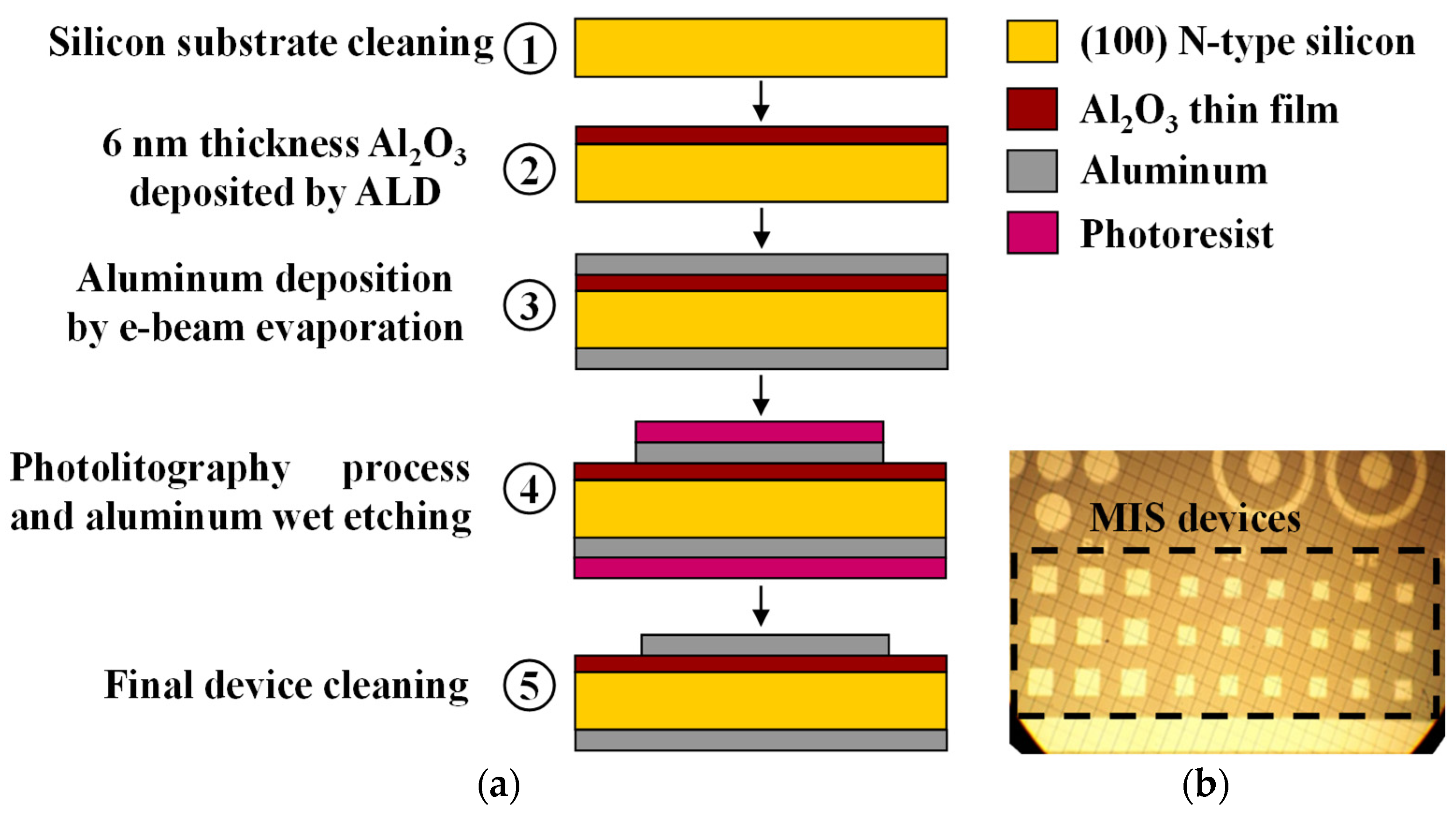
Figure 1a shows a schematic diagram of the fabrication process of micrometric MIS devices. (1) First, a (100) n-type silicon wafer with 400 µm of thickness, is cleaned using hydrofluoric acid (HF) solution, acetone (CH
3(CO)CH
3), and standard RCA procedure. (2) A thin Al
2O
3 layer (thickness of 6 nm) is deposited using ALD technique at 250 °C for 8 min, with 40 working cycles, and a pressure of 0.2 Torr; aluminum and oxygen precursors were TMA (Trimethyl Aluminum) and water (H
2O) in the vapor phase, respectively. (3) An aluminum layer with 400 nm of thickness is deposited on top of the Al
2O
3 film by e-beam evaporation technique at pressure of 1 × 10
−7 torr and deposition rate of 20 Å/s. Then, the back (lower) side of the silicon wafer was metalized with 500 nm of aluminum, using the same deposition technique and conditions. This layer is used as the back electrode for the MIS devices. (4) The next step was a photolithography process at the upper metal surface to pattern the gate electrode for MIS devices. In this process, the positive photoresist was deposited by spin-coating at 4000 revolutions per minute (rpm) for 30 s, and then it was prebaked at 110 °C for 1 h. A photolithography mask was aligned to the sample, which was exposed for 2.2 s of UV radiation. Then, the positive photoresist exposed to UV radiation was removed with acetone. Wet etching with Al-etch (phosphoric, acetic and nitric acids, 25:7:1) solution at 40 °C for 2 min was applied to the exposed aluminum in order to define geometrical patrons for gate electrodes at different areas. (5) Finally, a cleaning step was undertaken with acetone on both sides of the sample.
Figure 1b shows a photograph of fabricated Al
2O
3 MIS devices.
3. Results
The gate current-gate voltage (
Ig-
Vg) measurements were performed with the Keithley 4200-SCS Semiconductor Parameter Analyzer for MIS devices with gate electrode areas of 3.6 × 10
−5 cm
2 (60 μm × 60 μm) and 6.4 × 10
−5 cm
2 (80 μm × 80 μm). For each fabricated structure, different measurements were developed in order to ensure reproducibility and confirm the high quality of the deposited ultrathin film of Al
2O
3. A gate voltage (
Vg) sweep was performed from 0 V to 5 V and inversely with a current compliance of 1 × 10
−3 A, as is shown in
Figure 2a.
Figure 2b depicts curves the measurements of gate current density (
Jg) versus electric field (
E) of the MIS devices. In these results, the gate current is higher for MIS devices with larger gate electrode areas. In addition, a breakdown voltage (
Vbd) occurs for higher gate voltage or electric field and higher gate electrode area, which has a dependence on traps density in the semiconductor/oxide interface [
14]. At
Vbd, a considerable amount of the atomic bonding of the Al
2O
3 is opened creating traps in its volume, allowing the flow of electrons to the gate electrode [
15]. After the breakdown voltage, an increment of
Ig or
Jg occurs, rising the current compliance that is established by the measurement equipment.
The current density-electric field (J-E) corresponding to Ig-Vg measured data of MIS devices were analyzed and modeled considering the dominant conduction mechanisms through ultrathin Al2O3 film, in which were found: ohmic conduction (OC) for low electric fields, Poole–Frenkel emission (PFE) and Schottky emission (SE) for moderate electric fields, and trap-assisted tunneling (TAT) for high electric fields.
3.1. Ohmic Conduction (OC)
Ohmic conduction is a bulk-limited conduction mechanism that considers the charge transport of both carriers, free electrons present in the conduction band, and holes in the valence band through the tunneling process. There exists a linear behavior of current density as a function of the electric field, according to Ohm’s law, which occurs in semiconductor devices. Due to a large oxide bandgap, a carrier charge generated for thermal excitation could be presented [
16]. In addition, OC is reported for a small electric field; thus, its current density is small too.
Figure 3a shows a schematic representation of band energy for this mechanism. The current density because of ohmic conduction is given by:
where
σ is the conductivity of oxide film,
E is the electric field,
q is electron charge,
μ is electron mobility, and
n is the electron density in conduction band determined by:
where
NC is the effective state density in the conduction band,
kB is Boltzmann constant,
T is the temperature in Kelvins,
EC is conduction band energy, and
EF is the Fermi energy level.
Figure 3b compares
J-
E measured and modeled curves for MIS devices with a gate electrode area of 3.6 × 10
−5 cm
2 and 6.4 × 10
−5 cm
2 for small electric fields. For
E < 1.75 MV/cm, the current density has a linear behavior because the ohmic conduction is dominant; the model gets a good match with measured data. According to the results, an average conductivity of 7.7 × 10
−16 S/cm was extracted, which is similar to that reported in [
17] for an electron mobility (
μ) of 2.4 × 10
−4 cm
2/V·s. For
E > 1.75 MV/cm, the current density increases due to other conduction mechanisms, such as Poole–Frenkel or Schottky emission.
3.2. Poole–Frenkel Emission (PFE)
PFE is a bulk-limited conduction mechanism that depends on the dielectric film’s trap energy levels. PFE involves the emission of electrons by thermal excitation present in traps with an energy level into the conduction band of the dielectric film. The Coulombic potential energy of electrons moving from traps into oxide can be reduced by an applied electric field, which increases the probability of an electron thermally excited out of the trap into the conduction band of the dielectric film, as is shown in
Figure 4a. The current density due to this conduction mechanism is calculated by:
where
ϕT is the trap energy level into the oxide,
ε0 is the vacuum permittivity, and
εox is the optical dielectric constant. Moreover,
Figure 4b shows a comparison of experimental data and PFE model plotted as
Ln(
J/
E) versus
E1/2, at 300 °K, according to Equation (3), evidencing a linear behavior. The average value for the energy trap (
ϕT) is extracted from the slope of the linear regression, which is obtained by:
The average extracted value for
ϕT is 1.52 eV, which is related to energy below the conduction band due to defects in the oxide, such as oxygen vacancies and dangling bonds. On the other hand, the average oxide relative permittivity (
εox) extracted from the same expression is 7.57, which is an admissible value for Al
2O
3 in the amorphous phase [
18,
19]. For this conduction mechanism in its own materials, first, electrons are transferred from the conduction band of n type silicon to this trap energy level in the Al
2O
3 band gap via a tunneling process. Then, those electrons are transferred to the conduction band of Al
2O
3 by a thermal excitation process.
3.3. Schottky Emission (SE)
SE is an electrode-limited conduction mechanism that is present if the electrons can gain enough energy through thermal activation to overcome the energy barrier (
qϕB) and get into the dielectric, as is shown the energy band diagram in
Figure 5a. The energy barrier height at the semiconductor-dielectric interface may be lowered by the image force, which is called the Schottky effect. The equation for Schottky emission is determined by:
where
A* is the effective Richardson constant obtained by
A* = 4π
qk2m*/
h3 = 120
m*/
m0. Here,
m0 is the free electron mass,
m* is the effective electron mass in the oxide layer,
T is the absolute temperature,
kB is the Boltzmann constant, and
h is the plank constant.
Figure 5b shows the measurement results of
J/
T2 as a function
E1/2 compared with the Schottky model. These results show a linear fit for electric field of 1 MV/cm to 2 MV/cm, which indicates the presence of this mechanism for the measured electric field range. According to Equation (4), the average barrier energy level (
ϕB) level can be extracted from the slope of linear regression, which is reported by:
The average extracted value for ϕB at 300 K is 2 eV.
3.4. Trap Assisted Tunneling (TAT)
TAT is a bulk-limited conduction mechanism in which electrons will go through the dielectric film assisted by trap energy levels generated into the oxide due to high electric fields. Those traps split the energy barrier into two parts, allowing consecutive tunneling through thinner energy barriers and increasing the probability of the total tunneling process. The TAT process can be elastic if the electron is trapped and then tunnels through the barrier and no kinetic energy is lost. Thus, the particle momentum is conserved (
Figure 6a-(i)). It can be inelastic if the electron is trapped in a trapping center and then relaxes (loses energy) to another trap center (
Figure 6a-(ii)). The current density of this inelastic TAT mechanism is approximated by:
where
Nt is the traps density into the oxide,
Ct is a slowly varying function of electron energy and
ϕt is the trap energy level.
Figure 6b shows the measured and modeled curves
Log(
JE) versus 1/
E to plot the TAT conduction mechanism. According to Equation (7), the energy trap level,
ϕt, can be extracted from the slope of linear fitting, which is given by:
where the average value for
ϕt at 300 K is 1.36 eV, which is the energy trap that could be due to state density caused by oxygen vacancies present in the valence band of the dielectric film [
20].
Based on the
J-
E measured data to extract electrical properties of Al
2O
3 layer and according to the predominant conduction mechanism, an approximation of the total current model (sum of ohmic conduction, Poole–Frenkel emission, trap-assisted tunneling, and Schottky emission) can be estimated as:
where
E is the electric field, (1 ±
Axtanh(
E))/2 is a function used to unify separated CM models,
A1,
A2,
A3 and
A4 are fitting parameters.
3.5. Numerical Simulations
Figure 7 illustrates a schematic diagram of the cross-section of the MIS structure that is generated and simulated with Atlas tool from Silvaco TCAD. This structure consists of a n-type silicon substrate (300 μm of thickness) with doping of 1 × 10
15 atoms/cm
3, an Al
2O
3 film with 6 nm of thickness, and an aluminum layer (400 nm of thickness) for the gate electrode. In addition, we included a semiconductor/oxide interface charge of 1 × 10
12 eV
−1cm
−1, which is a value commonly reported [
9]. To analyze the MIS structure and compute the current density, we used the SRH (Shockley–Read–Hall), Lombardi (CVT), and Quantum models, considering an integration area along the semiconductor/oxide interface.
Figure 8 depicts the results of the measured current density, the total current density (
JTOTAL) calculated by Equation (8), and the simulated current density (
JSIM) as a function of the electric field for MIS capacitors with Al
2O
3 layer (6 nm of thickness) deposited by ALD. These results show a good match between the measured data with the proposed model and simulations models for a wide range of electric fields before the breakdown occurs, lower than 6 MV/cm.
Finally,
Table 1 summarizes the main physical and electrical parameters extracted by the analysis of dominant CMs in our MIS capacitors, as well as the fitting parameter used in the proposed current density model.
4. Discussion
The results obtained from the analysis of the I-V measurements to Al
2O
3 MIS Capacitors using different conduction mechanisms, such as ohmic conduction, Poole–Frenkel emission, Schottky emission, or trap-assisted tunneling, were consistent according to values reported in different works [
10,
14,
17,
20]. The energy due to traps present in the bulk of Al
2O
3 considering its conduction band (
ϕT) was 1.52 eV, which is similar to that reported in [
13], where the authors fabricated MIS devices with the same materials and deposition techniques. The
ϕT is strongly linked to an excess of oxygen atoms and ions, which are generated during the deposition of ultrathin Al
2O
3films on n-type silicon wafer by ALD [
13], since there are OH groups at the interface with the semiconductor, and the presence of an ultrathin SiO
x layer. On the other hand, the trap energy extracted by TAT analysis is because of electron trapping by the defect density related with oxygen vacancies in the Al
2O
3 bulk, which could be amorphous or crystalline [
21], generated during the deposition process. In addition, the height of the barrier extracted by Schottky emission analysis,
ϕB, is 2 eV, which is similar to that reported in [
22], at 250 °C as the maximum deposition temperature. This parameter brings information about the defect’s density in the metal/dielectric interface in the MIS capacitor.


 ,
, 


