Communication

Single-Layer Interconnected Magneto-Electric Dipole Antenna Array for 5G Communication Applications

College of Electronics and Information Engineering, Harbin Institute of Technology (Shenzhen), Shenzhen 518055, China
*
Author to whom correspondence should be addressed.
Electronics 2023, 12(4), 922; https://doi.org/10.3390/electronics12040922
Submission received: 16 January 2023 / Revised: 8 February 2023 / Accepted: 9 February 2023 / Published: 12 February 2023

Abstract

:
A high-gain and wideband interconnected magneto-electric (ME) dipole on a single-layer PCB substrate is designed for 5G communication applications. Microstrip lines and coplanar striplines (CPSs) serve as transmission lines to connect the ME dipole elements along the E-plane and the H-plane directions, respectively. Impedance matching and sidelobe-level suppression are the key challenges to design a large-scale interconnected ME dipole antenna array. It is shown that impedance matching can be improved by introducing slots and adjusting the width of microstrip lines. Sidelobe level can be enhanced by properly choosing the length of the microstrip lines. A 5 × 5 interconnected ME dipole array is fabricated on a single layer of the RT/duroid 5880 substrate. The proposed antenna exhibits a measured −10 dB impedance bandwidth of 14.5 GHz (52% at 28 GHz) and a maximal peak realized gain of 20.44 dBi at 27.5 GHz with a 3 dB gain bandwidth of 3.5 GHz (12.5% at 28 GHz). The proposed antenna array is a good candidate for 5G communication applications due to its advantages of simple feeding structure, wide bandwidth, high gain, and low profile.

1. Introduction

In recent years, 5G communication has received ever-increasing attention from both academia and industries due to its high data rates, high reliability, and low delay compared to conventional communication networks. Since a huge unlicensed frequency spectrum can be provided by the millimeter-wave band, millimeter-wave antennas with high gain and wide bandwidth are highly demanded for 5G communication applications. In the past few years, many millimeter antennas were reported for 5G communication applications [1,2,3,4,5,6,7]. Among them, magneto-electric (ME) dipole is a good antenna candidate for 5G communication applications. The magneto-electric dipole model, with a significant impact, was first proposed as an antenna element by Kwai Man LUK in 2006 [8]. This new type of combined antenna can achieve a wide impedance bandwidth, symmetrical radiation patterns in the E plane and H planes, stable gain performance in the operating frequency band, and low backward radiation. Since the first publication, several ME dipole antenna arrays have been reported [9,10,11,12,13,14,15,16,17,18,19,20,21]. In 2018, Zhang-Cheng Hao and Quan Yuan et al. proposed a double-layer magneto-electric dipole array structure, which was fed by a substrate-integrated waveguide (SIW) and combined with aperture coupling [9]. This structure achieves wide bandwidth and maximal peak realized gain due to the low loss characteristics of SIW and the broadband performance of ME dipole. In 2020, a millimeter-wave substrate-integrated ME dipole, which is excited by a microstrip feeding structure, was proposed in [10]. It radiates linearly polarized waves and can cover the 22–33 GHz band. Although the structures in [9] and [10] have good performance, they suffered from a complex feeding network and high cost. A differentially driven transmission-line-excited ME dipole was designed in [11,12,13]. The 2 × 2 ME dipole array surrounded by a rectangular cavity can achieve an impedance bandwidth of 29.2% and a broadside gain from 10.9 to 13.7 dBi. However, it lacks the flexibility to scale to a 2-D large antenna array.
In this paper, we present, for the first time, a single-layer interconnected ME dipole antenna array, and demonstrate the capability to scale the array in two dimensions. We show that the proposed antenna array can achieve high gain and wide bandwidth with a simple feeding structure for the millimeter-wave point-to-point communication application. The wide bandwidth of the proposed antenna array helps to achieve high data rates for 5G applications. The high propagation attenuation in the millimeter-wave band can be compensated by the high gain of the proposed antenna array [22]. In Section 2, the antenna configuration and the working mechanism are depicted. We enhance the impedance matching by cutting a slot on the coplanar stripline and adjusting the width of the microstrip lines. The sidelobe level is suppressed by specifically choosing the length of the microstrip lines. In Section 3, a 5 × 5 interconnected ME dipole antenna array at 28 GHz is fabricated and measured to confirm the feasibility of the interconnected ME dipole antenna array scheme. Finally, a conclusion is given in Section 4.

2. Design Procedure

2.1. Antenna Configuration

The configuration of the proposed interconnected ME dipole is shown in Figure 1. The total size of the proposed antenna is 43 × 50 mm2 (4λ × 4.67λ), where λ is the free-space wavelength at 28 GHz. The proposed antenna consists of two metallic layers and one dielectric layer. The radiators, which are composed of 5 × 5-optimized ME dipole elements, are on a Rogers RT/duroid 5880 with εr = 2.2, tan δ = 0.009, and thickness of 1.57 mm. The metallic patches work as electric dipoles and the shorted metalized vias at the inner edge of each half planar dipole form magnetic dipoles. An L-shaped probe, which is composed of a via and a small patch is arranged near the geometrical center of the interconnected ME dipole radiator, which is utilized to excite the planar dipoles and the vertically quarter-wave shorted patch antenna simultaneously. The feeding via, together with the adjacent three shorted vias, accomplish a coplanar waveguide (CPW) line to transmit signals to the small patch. Electrical energy is coupled from the small patch through the gap to the antenna element. The diameter of the vias is 0.6 mm. The coplanar striplines (CPSs) are used to excite the ME dipole elements along the x-direction and the microstrip lines are used to transmit the signal to the radiating elements along the y-direction. A metallic ground plane is on the backside of the dielectric substrate. Dimensions of the antenna are detailed in Table 1.

2.2. Interconnected ME Dipole Array Working Mechanism

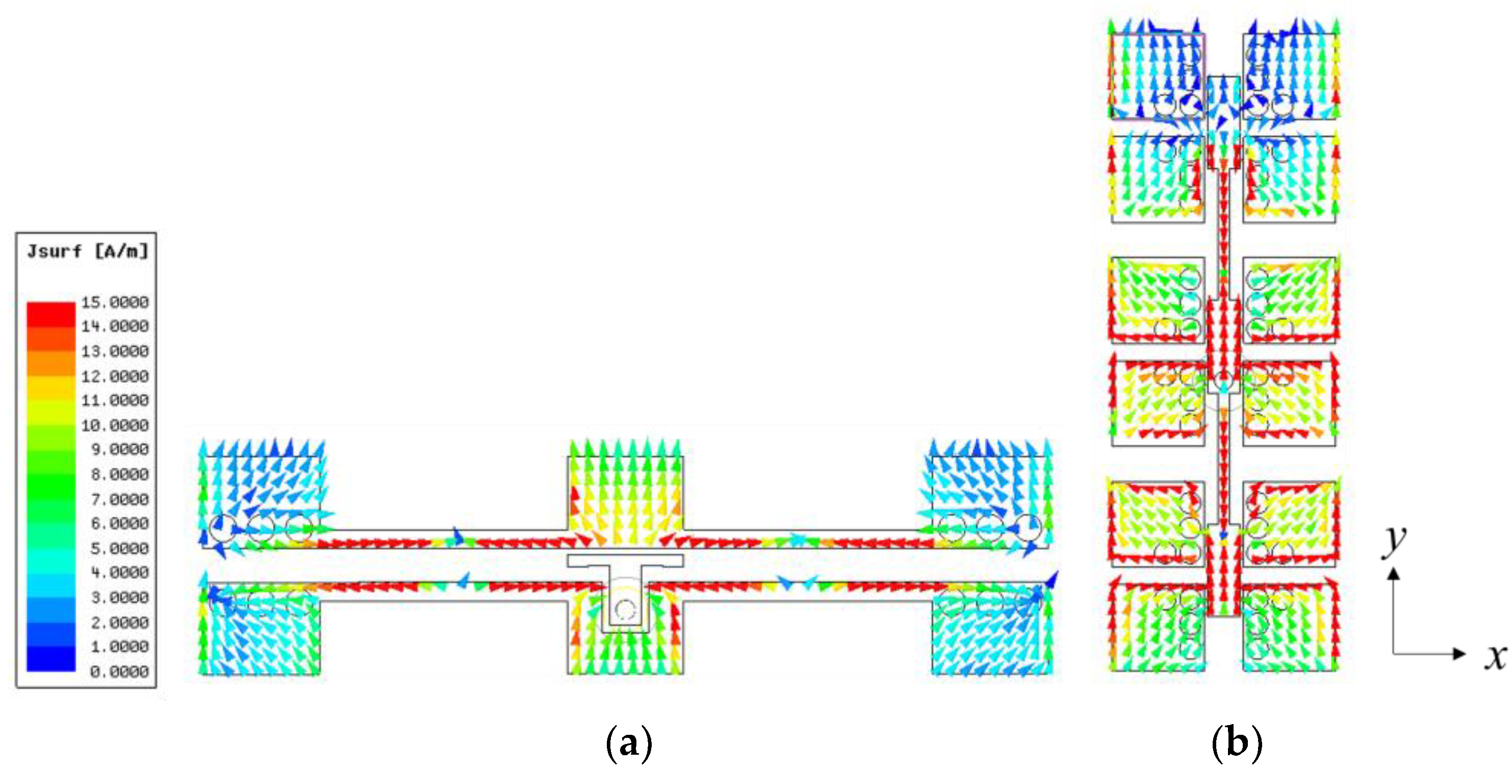
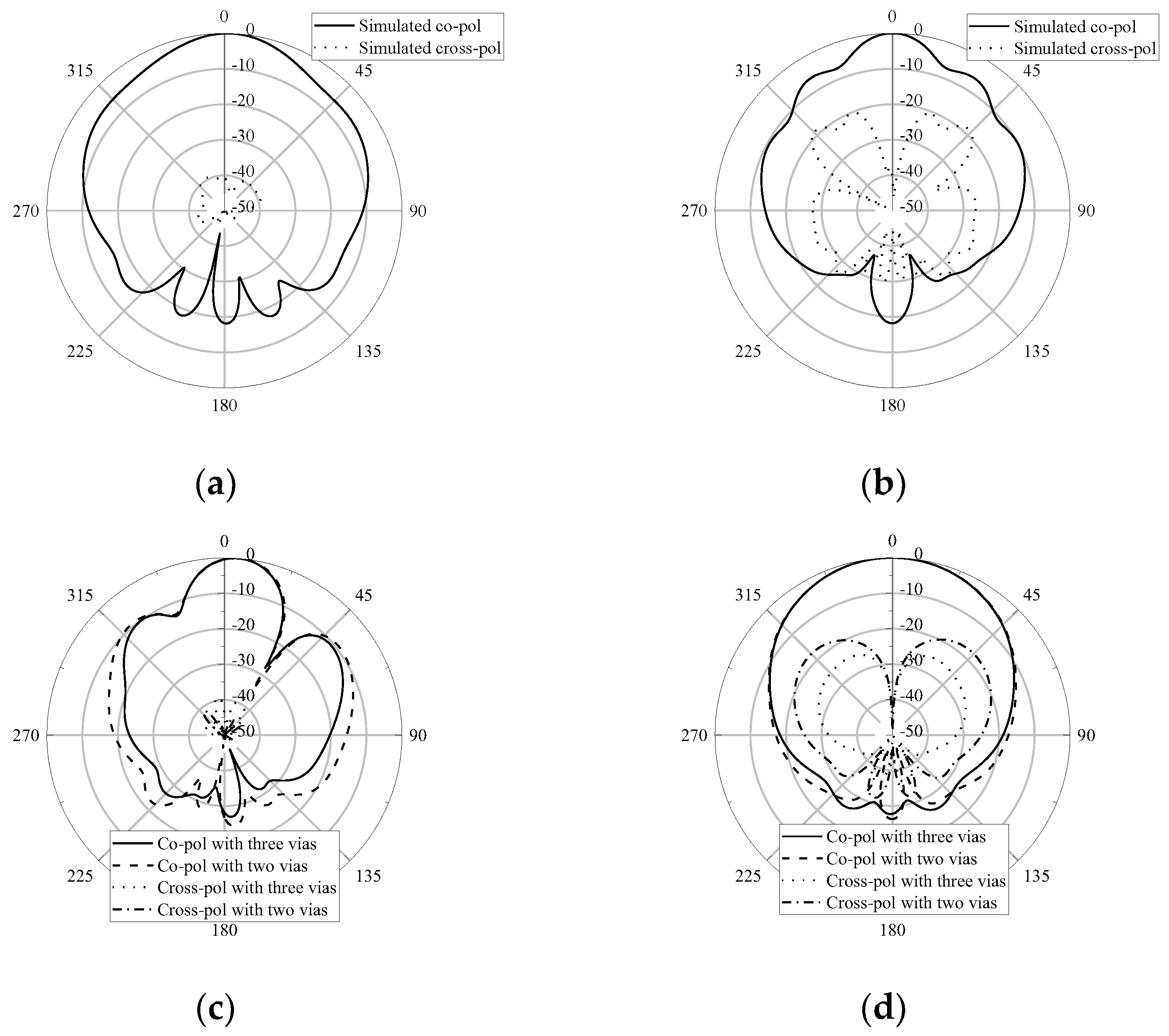
To obtain a uniform current distribution on the ME dipole elements, the length of the CPS should be approximately one guided wavelength λg, and the length of the microstrip line should be approximately λg/2. The current distributions of the 1-D 3 × 1 interconnected ME dipole array along the x-direction and the 1-D 1 × 3 interconnected ME dipole array along the y-direction are depicted in Figure 2a and Figure 2b, respectively. It is shown that the currents are almost in phase on the ME dipole elements and are out of phase on the CPS, which results in a main beam in the broadside direction and a weak cross polarization in the H plane, as shown in Figure 3. It should be mentioned that three vias are specifically arranged at the inner edge of the 1-D 1 × 3 interconnected ME dipole array along the y-direction to reduce the interference from the interconnected transmission lines to the ME dipole elements. It can be seen in Figure 3, c and d, that the sidelobe level in the E plane, and the cross-polarization level in the H plane of the 1-D 1 × 3 interconnected ME dipole array along the y-direction, decrease as the number of vias at the inner edge increases from two to three.

2.3. Impedance-Matching Techniques of 1-D Interconnected ME Dipole Antenna Array

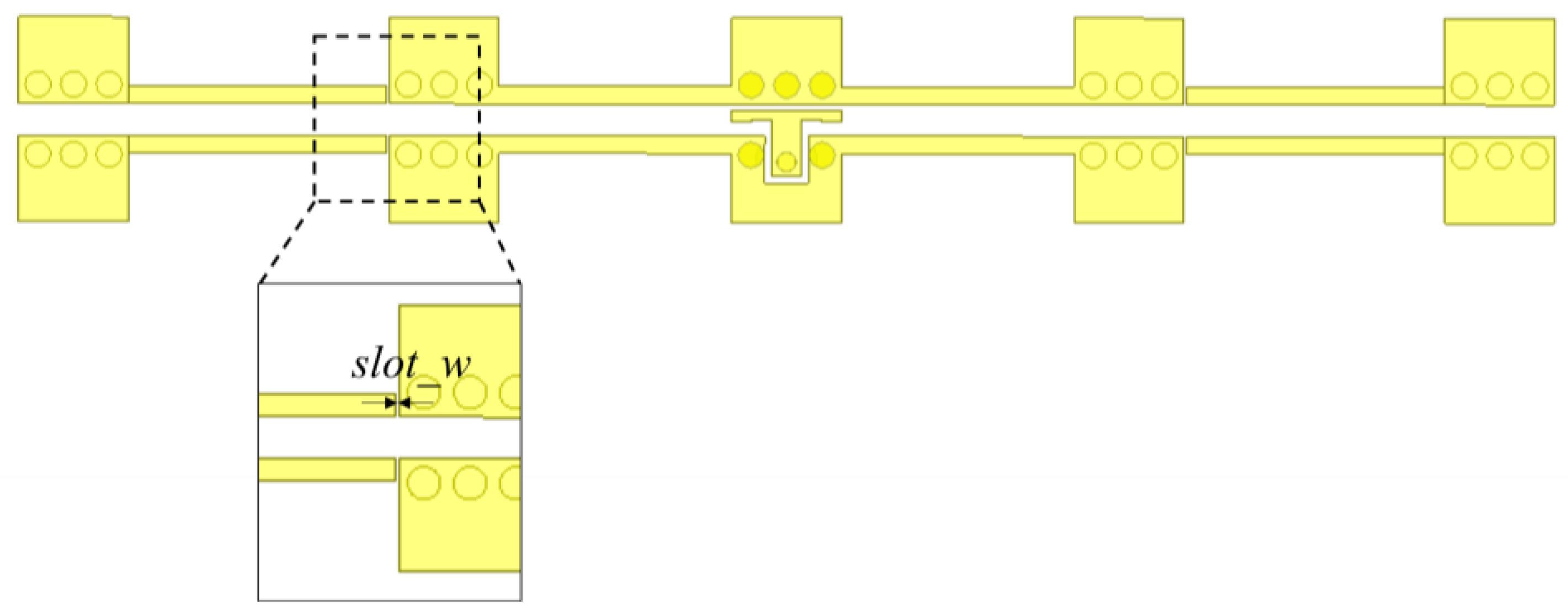
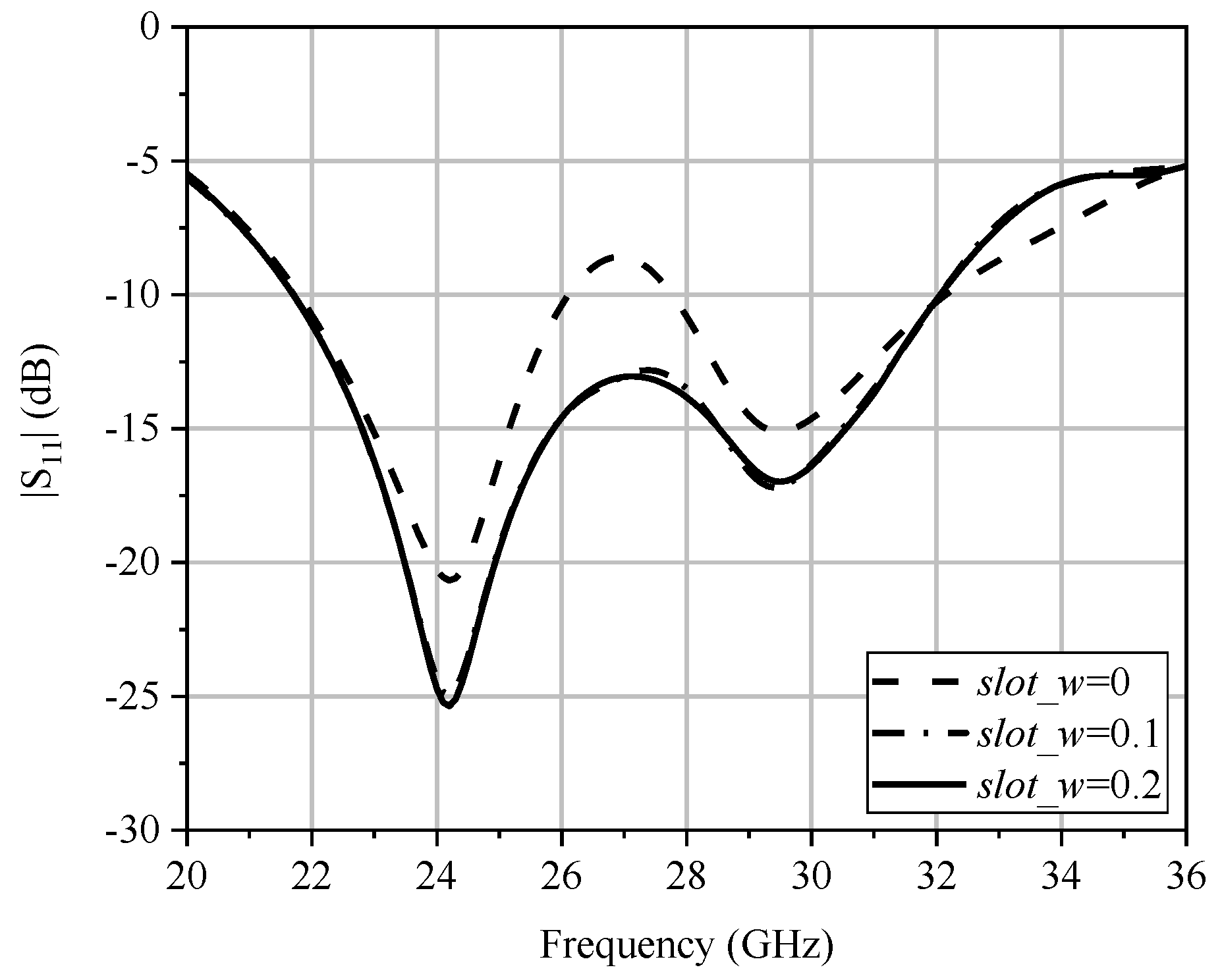
Impedance matching is the key challenge in designing 1-D interconnected ME dipole antenna arrays with large sizes. The ME dipole elements along the H-plane direction are excited by the CPS lines, which introduce additional inductance to the input impedance of the antenna array, leading to poor matching at the input port. A slot is cut between the CPS line and the ME dipole element to introduce additional capacitance to the input impedance, as shown in Figure 4. The input impedance at the input port of a 5 × 1 interconnected ME dipole array for the first-order approximation can be expressed as shown in Figure 5, where Cslot is the capacitance, which is introduced by the slot and the R is the radiation resistance of the ME dipole element. Figure 6 shows the simulated |S11| of the 5 × 1 interconnected ME dipole array. Note that the |S11| decreases from −8 to −13 dB as the width of the slot increases from 0 mm to 0.2 mm, while the resonant frequency basically remains invariable.
For the 1-D interconnected ME dipole array along the E plane, the width of the microstrip line is of importance to control the input impedance. As the number of radiating elements along the E-plane direction increases, the capacitance between the feeding patch and the shorted vias at the inner edge of the electric dipole increases, which can be compensated by increasing the inductance of the microstrip line. Figure 7 shows the input impedance of a 1 × 5 interconnected array along the E plane. Note that the |S11| value decreases from −5 dB to −11 dB as the width of the microstrip line decreases from 0.1 mm to 0.4 mm, and the resonant frequency basically remains invariable.

2.4. 2-D Interconnected ME Dipole Antenna Array

The 2-D interconnected ME dipole array consists of 1-D interconnected ME dipole arrays along the x-direction and the y-direction. The input impedance of the 1-D interconnected ME dipole array along the x-direction can be expressed as R/n1 for the first-order approximation, while the input impedance of the 1-D interconnected ME dipole array along the y-direction can be given as R × n2, where R is the radiation resistance of ME dipole elements and the n1 and n2 are the numbers of the ME dipole elements along the x-direction and that along the y-direction, respectively. The input impedance matching of the 2-D interconnected ME dipole array can be easily achieved without introducing additional matching structures when n1 equals n2. Figure 8 shows the |S11| of the 1-D 3 × 1 interconnected ME dipole array along the x-direction, 1-D 1 × 3 interconnected ME dipole array along the y-direction, and the 2-D 3 × 3 interconnected ME dipole array. The parameters of the ME dipole elements and the interconnected transmission lines for the 2-D 3 × 3 interconnected ME dipole array in Figure 3 are the same as those of 1-D three-element interconnected ME dipole arrays. The simulated −10 dB impedance bandwidths are 11.66 GHz (41.6% at 28 GHz) from 23.17 GHz to 34.83 GHz, 8.6 GHz (30.7% at 28 GHz) from 22.5 GHz to 31.10 GHz, and 11.72 GHz (41.9% at 28 GHz) from 23.44 GHz to 35.16 GHz for the 3 × 1 interconnected ME dipole array, the 1 × 3 interconnected ME dipole array and the 2-D 3 × 3 interconnected ME dipole array, respectively.

2.5. Sidelobe-Level Enhancement

The conventional interconnected antenna array requires that the microstrip lines be λg/2 at the center frequency of operation. Thus, the current distribution at any instant would be in phase on the ME dipole elements. Unsynchronized current distribution was observed in the ME dipole elements far away from the feeding point, leading to a high sidelobe level in the E plane. The unsynchronized current is caused by the phase asynchronization of the far ME dipole elements from the feeding point. The current distribution can be improved effectively by modifying the length of microstrip lines. Figure 9 shows the simulated co-polarization radiation patterns in the E plane at 28 GHz versus l. It can be found that the sidelobe level is decreased from −6 dB to −15 dB as the l is changed from 8 mm to 7 mm.

3. Results and Discussion

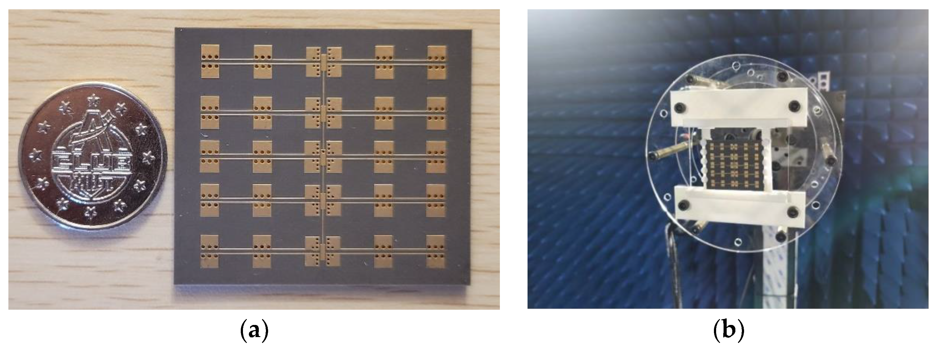
The photographs of the fabricated 5 × 5 interconnected ME dipole antenna array are shown in Figure 10. A W-type connector (from Lair Microwave L24FS38F04) is launched underneath the ground plane. Measurements on impedance bandwidth, gain, and radiation patterns were conducted with a millimeter wave band network analyzer (Rohde and Schwarz ZNA 67) and an in-house far field millimeter wave antenna measurement system. The gain in the proposed antenna array was obtained using the comparison method. The antenna is excited by coaxial cable and mounted on a 3D-printed fixture. The fixture is covered by an absorber during the measurement.
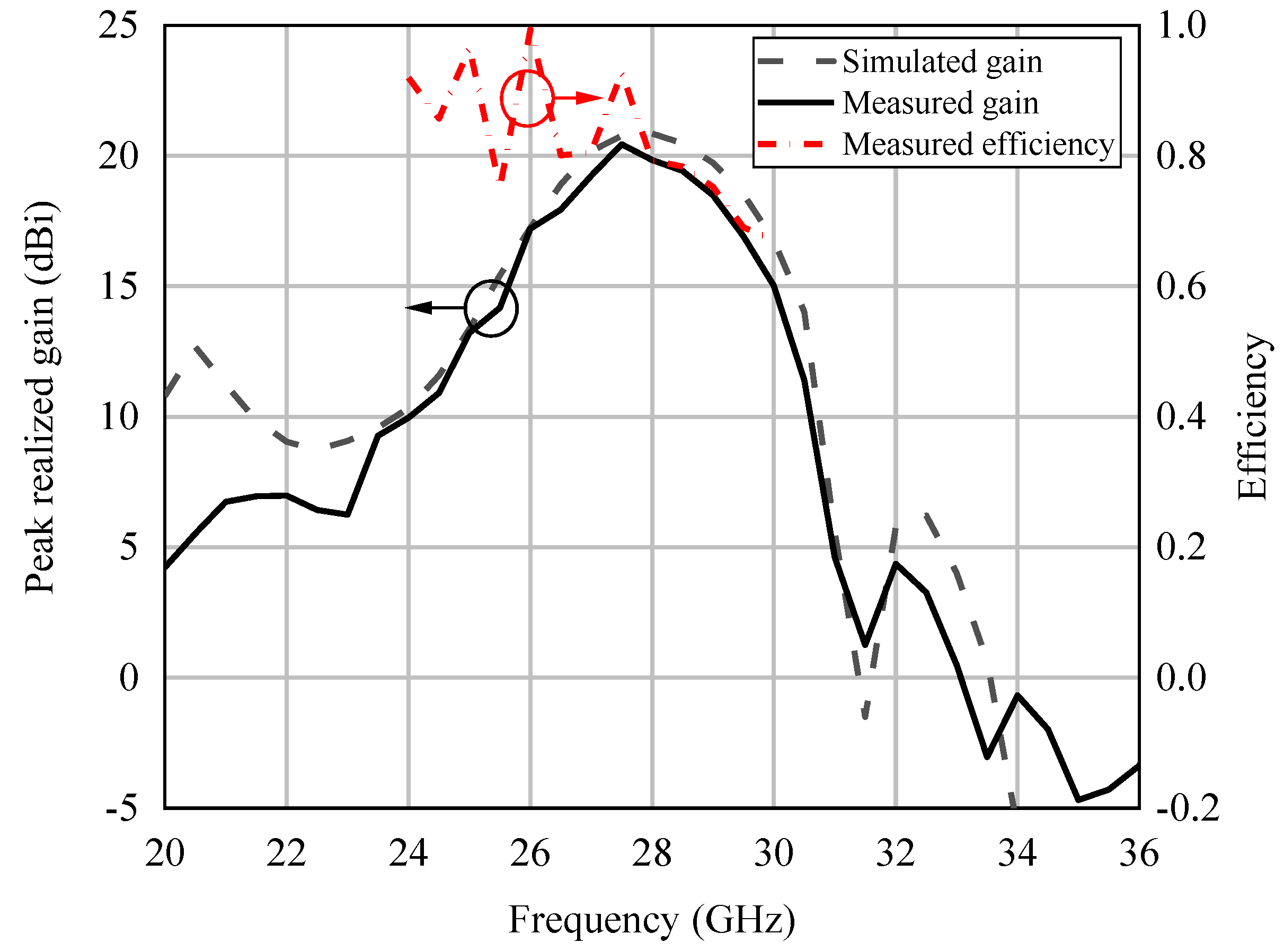
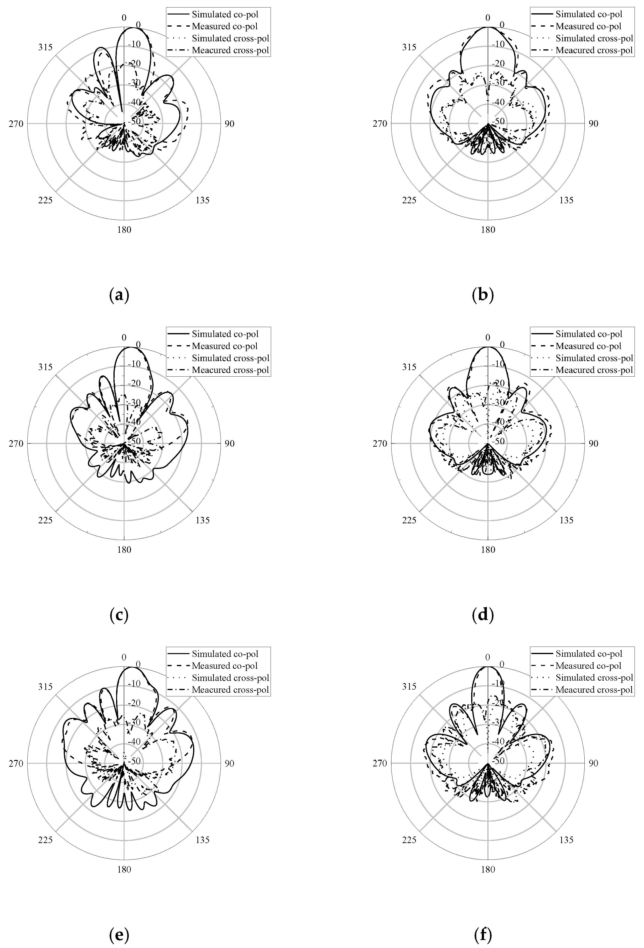
Figure 11 shows the simulated and measured |S11|, which are in good agreement. The simulated and measured −10 dB impedance bandwidths are 11.9 GHz (or 42.5% at 28 GHz) from 22.7 to 34.6 GHz and 14.5 GHz (or 52% at 28 GHz) from 21.5 GHz to 36 GHz, respectively. The discrepancy between the simulated and measured |S11| is mainly due to the effect of fabrication tolerance and the soldering. Figure 12 plots the simulated and measured peak realized gain and efficiency. The simulated and measured maximum realized gains are 20.85 dBi at 28 GHz and 20.44 dBi at 27.5 GHz, respectively. The simulated and measured 3 dB gain bandwidths are 3.65 GHz (or 13% at 28 GHz) from 26.18 GHz to 29.69 GHz and 3.5 GHz from 26.25 GHz to 29.75 GHz (or 12.5% at 28 GHz), respectively. By comparing the measured gain and the simulated directivity, the radiation efficiency of the proposed antenna array is 79.25% at 28 GHz. The simulated and measured radiation patterns are shown in Figure 13. The main beams of the radiation patterns are in the broadside direction, and the cross-polarization levels are low in both the E plane and the H plane. The simulated and measured half-power beamwidths of the radiation beam in the E plane at 28 GHz are 15° and 14.5°, respectively. The simulated and measured half-power beamwidths in the H plane at 28 GHz are 14.5° and 14°, respectively. The measured co-pol radiation patterns agree well with the simulated radiation patterns. A comparison between our work and the design in other works is shown in Table 2. Note that the interconnected ME dipole antenna array in this work has the advantage of low profile, wide bandwidth, and high gain over other reported antennas in the references.

4. Conclusions

A new interconnected ME dipole array antenna on a single layer of a Rogers 5880 substrate was developed for 5G communication applications. In the proposed design, microstrip lines and CPS lines are used to transmit the energy to the ME dipole elements along the E-plane and the H-plane directions, respectively. The input impedance matching can be improved by adding a slot on the CPS lines, adjusting the width of the microstrip lines, and choosing a proper array topology. Unequal length of the transmission is utilized to achieve a uniform current distribution on the ME dipole elements. The proposed antenna exhibited a measured impedance bandwidth of 52%, a measured maximum realized gain of 20.44 dBi at 27.5 GHz, and a 3 dB gain bandwidth of 12.5% at 28 GHz. It showed good radiation patterns with small cross-polarization radiation.

Author Contributions

Conceptualization, Z.C. and K.W.; methodology, Z.C. and W.Z.; software, W.Z.; validation, Z.C. and W.Z.; formal analysis, K.W.; investigation, K.W.; resources, Z.C.; data curation, W.Z.; writing—original draft preparation, Z.C. and W.Z.; writing—review and editing, K.W.; visualization, Z.C.; supervision, K.W.; project administration, Z.C. All authors have read and agreed to the published version of the manuscript.

Funding

This research was funded, in part, by the National Natural Science Foundation of China under Grant 61901139, 62001140, in part, by Shenzhen Science and Technology Program under Grant KQTD20210811090116029, in part, by the National Key Research and Development Program of China under Grant 2020YFB1807303, and, in part, by the Shenzhen Basic Research Program under Grant GXWD20201230155427003-20200824201212001.

Institutional Review Board Statement

Not applicable.

Informed Consent Statement

Not applicable.

Data Availability Statement

The data presented in this study are available on request from the corresponding author.

Conflicts of Interest

The authors declare no conflict of interest.

References

  1. Han, W.; Yang, F.; Ouyang, J.; Yang, P. Low-cost wideband and high-gain slotted cavity antenna using high-order modes for mil-limeter-wave application. IEEE Trans. Antennas Propag. 2015, 63, 4624–4631. [Google Scholar] [CrossRef]
  2. Park, S.J.; Shin, D.H.; Park, S.O. Low side-lobe substrate-integrated-waveguide antenna array using broadband unequal feeding network for millimeter-wave handset device. IEEE Trans. Antennas Propag. 2016, 64, 923–932. [Google Scholar] [CrossRef]
  3. Dzagbletey, P.A.; Kim, K.S.; Byun, W.J.; Jung, Y.B. Stacked microstrip linear array with highly suppressed side-lobe levels and wide bandwidth. IET Microw. Antennas Propag. 2017, 11, 17–22. [Google Scholar] [CrossRef]
  4. Dzagbletey, P.A.; Jung, Y.B. Stacked microstrip linear array for millimeter-wave 5G baseband communication. IEEE Antennas Wirel. Propag. Lett. 2018, 17, 780–783. [Google Scholar] [CrossRef]
  5. Jin, H.; Che, W.; Chin, K.-S.; Yang, W.; Xue, Q. Millimeter-Wave TE20-Mode SIW Dual-Slot-Fed Patch Antenna Array With a Compact Differential Feeding Network. IEEE Trans. Antennas Propag. 2017, 66, 456–461. [Google Scholar] [CrossRef]
  6. Islam, S.; Zada, M.; Yoo, H. Highly Compact Integrated Sub-6 GHz and Millimeter-Wave Band Antenna Array for 5G Smartphone Communications. IEEE Trans. Antennas Propag. 2022, 70, 11629–11638. [Google Scholar] [CrossRef]
  7. Islam, S.; Zada, M.; Yoo, H. Low-Pass Filter Based Integrated 5G Smartphone Antenna for Sub-6-GHz and mm-Wave Bands. IEEE Trans. Antennas Propag. 2021, 69, 5424–5436. [Google Scholar] [CrossRef]
  8. Luk, K.M.; Wong, H. A new wideband unidirectional antenna element. Int. J. Microw. Opt. Technol. 2006, 1, 35–44. [Google Scholar]
  9. Hao, Z.-C.; Yuan, Q.; Li, B.-W.; Luo, G.Q. Wideband W-Band Substrate-Integrated Waveguide Magnetoelectric (ME) Dipole Array Antenna. IEEE Trans. Antennas Propag. 2018, 66, 3195–3200. [Google Scholar] [CrossRef]
  10. Xu, J.; Hong, W.; Jiang, Z.H.; Zhang, H. Millimeter-Wave Broadband Substrate Integrated Magneto-Electric Dipole Arrays With Corporate Low-Profile Microstrip Feeding Structures. IEEE Trans. Antennas Propag. 2020, 68, 7056–7067. [Google Scholar] [CrossRef]
  11. Ruan, X.; Ng, K.B.; Chan, C.H. A differentially fed transmission-line-excited magnetoelectric dipole antenna array for 5G applications. IEEE Trans. Antennas Propag. 2018, 66, 5224–5230. [Google Scholar] [CrossRef]
  12. Ruan, X.; Chan, C.H. A Circularly Polarized Differentially Fed Transmission-Line-Excited Magnetoelectric Dipole Antenna Array for 5G Applications. IEEE Trans. Antennas Propag. 2019, 67, 2002–2007. [Google Scholar] [CrossRef]
  13. Ruan, X.; Wang, K. A Transmission Line Transition to Extend the Transmission-Line-Excited Magnetoelectric Dipole Antenna Array. IEEE Antennas Wirel. Propag. Lett. 2022, 21, 863–867. [Google Scholar] [CrossRef]
  14. Zhu, Q.; Ng, K.B.; Chan, C.H.; Luk, K.M. Substrate-integrated-waveguide-fed array antenna covering 57–71 GHz band for 5G ap-plications. IEEE Trans. Antennas Propag. 2017, 65, 6298–6306. [Google Scholar] [CrossRef]
  15. Chen, W.; Yu, Z.; Zhai, J.; Zhou, J. Developing wideband dual-circularly polarized antenna with simple feeds using magneto-electric dipoles. IEEE Antennas Wirel. Propag. Lett. 2020, 19, 1037–1041. [Google Scholar] [CrossRef]
  16. Ge, L.; Luk, K.M. A Three-Element Linear Magneto-Electric Dipole Array With Beamwidth Reconfiguration. IEEE Antennas Wirel. Propag. Lett. 2014, 14, 28–31. [Google Scholar] [CrossRef]
  17. Ge, L.; Luk, K.-M. Linearly Polarized and Dual-Polarized Magneto-Electric Dipole Antennas With Reconfigurable Beamwidth in the H-plane. IEEE Trans. Antennas Propag. 2015, 64, 423–431. [Google Scholar] [CrossRef]
  18. Yang, S.J.; Pan, Y.M.; Zhang, Y.; Gao, Y.; Zhang, X.Y. Low-Profile Dual-Polarized Filtering Magneto-Electric Dipole Antenna for 5G Applications. IEEE Trans. Antennas Propag. 2019, 67, 6235–6243. [Google Scholar] [CrossRef]
  19. Zhang, Y.; Zhang, X.Y.; Liu, Q.H. Dual-polarized filtering magnetoelectric dipole antenna utilizing intrinsic highpass filter network and integrated lowpass filter network. IEEE Trans. Antennas Propag. 2021, 69, 8090–8099. [Google Scholar] [CrossRef]
  20. Li, Y.; Luk, K.M. 60-GHz dual-polarized two-dimensional switch-beam wideband antenna array of aperture-coupled magneto-electric dipoles. IEEE Trans. Antennas Propag. 2016, 64, 554–563. [Google Scholar] [CrossRef]
  21. Feng, B.; Chen, J.; Chung, K.L.; Wang, L.; Li, Y. Dual-Polarized Filtering Magneto-Electric Dipole Antenna Arrays With High Radiation-Suppression Index for 5G New Radio n258 Operations. IEEE Trans. Antennas Propag. 2021, 70, 3058–3063. [Google Scholar] [CrossRef]
  22. Ji, Z.; Sun, G.-H.; Wong, H. A wideband circularly polarized complementary antenna for millimeter-wave applications. IEEE Trans. Antennas Propag. 2022, 70, 2392–2400. [Google Scholar] [CrossRef]
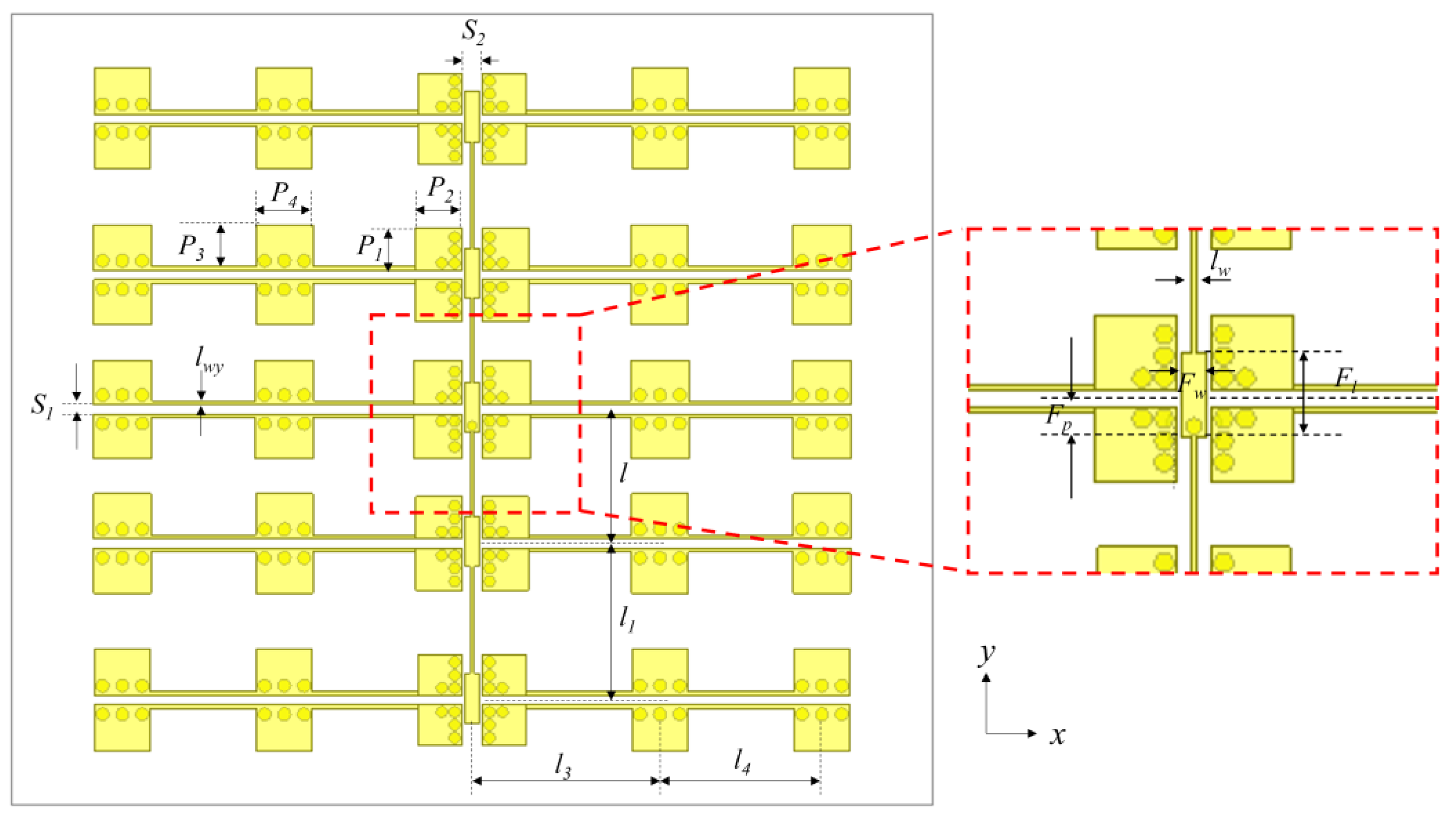
Figure 1. The 5 × 5 interconnected ME dipole antenna array configuration.
Electronics 12 00922 g001
Figure 2. Current distribution of (a) the 1-D 3 × 1 interconnected ME dipole array along the x-direction and (b) the 1-D 1 × 3 interconnected ME dipole array along the y-direction.
Electronics 12 00922 g002
Figure 3. Simulated radiations for the 1-D 3 × 1 interconnected ME dipole array along the x-direction (a) in the E plane at 28 GHz and (b) in the H plane at 28 GHz, and for the 1-D 1 × 3 interconnected ME dipole array along the y-direction (c) in the E plane at 28 GHz and (d) in the H plane at 28 GHz.
Electronics 12 00922 g003
Figure 4. The 1-D 5 × 1 interconnected ME dipole array with slot.
Electronics 12 00922 g004
Figure 5. The equivalent circuit for the half structure of 1-D 5 × 1 interconnected ME dipole array with slot.
Electronics 12 00922 g005
Figure 6. Simulated |S11| of the 5 × 1 interconnected ME dipole array versus slot w.
Electronics 12 00922 g006
Figure 7. Simulated |S11| of the 1 × 5 interconnected ME dipole array versus lw.
Electronics 12 00922 g007
Figure 8. Simulated |S11| of the 1-D 3 × 1 interconnected ME dipole array along the x-direction, 1-D 1 × 3 interconnected ME dipole array along the y-direction and the 2-D 3 × 3 interconnected ME dipole array.
Electronics 12 00922 g008
Figure 9. The simulated co-polarization radiation patterns in the E plane at 28 GHz versus l.
Electronics 12 00922 g009
Figure 10. Fabricated 5 × 5 interconnected ME dipole antenna array. The (a) fabricated prototype and (b) antenna under test.
Electronics 12 00922 g010
Figure 11. Simulated and measured |S11| versus frequency.
Electronics 12 00922 g011
Figure 12. Peak realized gain and efficiency versus frequency.
Electronics 12 00922 g012
Figure 13. Simulated and measured radiation patterns (a) at 27 GHz in the E plane, (b) at 27 GHz in the H plane, (c) at 28 GHz in the E plane, (d) at 28 GHz in the H plane, (e) at 29 GHz in the E plane, and (f) at 29 GHz in the H plane.
Electronics 12 00922 g013
Table 1. Interconnected ME dipole antenna array.
ParametersValue (mm)ParametersValue (mm)
Fl2.7Fp1
Fw0.8P12.4
P22.6P32.45
P43.1lw0.2
S10.5S21.1
l7.3l18.5
l310.2lwy0.2
l48.8
Table 2. Comparison of the proposed 5 × 5 interconnected ME dipole antenna array with related published works.
Ref.f0 (GHz)Radiating ElementAmount of SubstratesScaleImp. BW (%)Extension Ability3 dB Gain BW (%)Peak Gain (dBi)Overall Profile Height (mm)Size (λ × λ)
[1]32.3slot14 × 426No14.113.81.581.72 × 1.72
[2]28.45patch31 × 88Yes/13.972.0246.64 × 6.02
[3]27.85patch21 × 77.54Yes/14.711.078.92 × 1.88
[4]27.7patch26 × 76.3Yes5.421.81.076.88 × 8.27
[5]28patch34 × 48.5Yes8.519.11.53.92 × 3.55
[12]64.4ME dipole34 × 426.7Yes26.421.52.53.09 × 3.09
63.35ME dipole38 × 822.9Yes23.626.72.66.08 × 6.08
[7]45.05ME dipole22 × 236.6Yes36.612.21.0166 × 6
[13]84.25ME dipole28 × 413.9Yes13.8920.31.017/
[8]28.32ME dipole24 × 444.6Yes47.719.181.7372.83 × 2.83
27.7ME dipole28 × 844Yes44251.7385.54 × 5.54
This work28ME dipole15 × 552Yes12.520.441.574.00 × 4.67
“/” refers to the fact that the corresponding data are not given.
Disclaimer/Publisher’s Note: The statements, opinions and data contained in all publications are solely those of the individual author(s) and contributor(s) and not of MDPI and/or the editor(s). MDPI and/or the editor(s) disclaim responsibility for any injury to people or property resulting from any ideas, methods, instructions or products referred to in the content.