Article

Towards Machine Learning-Based FPGA Backend Flow: Challenges and Opportunities

1
College of Interdisciplinary Studies, Zayed University, Abu Dhabi P.O. Box 144534, United Arab Emirates
2
School of Engineering, University of Sunderland, Sunderland SR6 0DD, UK
*
Author to whom correspondence should be addressed.
These authors contributed equally to the work.
Electronics 2023, 12(4), 935; https://doi.org/10.3390/electronics12040935
Submission received: 12 January 2023 / Revised: 3 February 2023 / Accepted: 7 February 2023 / Published: 13 February 2023
(This article belongs to the Section Systems & Control Engineering)

Abstract

:
Field-Programmable Gate Array (FPGA) is at the core of System on Chip (SoC) design across various Industry 5.0 digital systems—healthcare devices, farming equipment, autonomous vehicles and aerospace gear to name a few. Given that pre-silicon verification using Computer Aided Design (CAD) accounts for about 70% of the time and money spent on the design of modern digital systems, this paper summarizes the machine learning (ML)-oriented efforts in different FPGA CAD design steps. With the recent breakthrough of machine learning, FPGA CAD tasks—high-level synthesis (HLS), logic synthesis, placement and routing—are seeing a renewed interest in their respective decision-making steps. We focus on machine learning-based CAD tasks to suggest some pertinent research areas requiring more focus in CAD design. The development of open-source benchmarks optimized for an end-to-end machine learning experience, intra-FPGA optimization, domain-specific accelerators, lack of explainability and federated learning are the issues reviewed to identify important research spots requiring significant focus. The potential of the new cloud-based architectures to understand the application of the right ML algorithms in FPGA CAD decision-making steps is discussed, together with visualizing the scenario of incorporating more intelligence in the cloud platform, with the help of relatively newer technologies such as CAD as Adaptive OpenPlatform Service (CAOS). Altogether, this research explores several research opportunities linked with modern FPGA CAD flow design, which will serve as a single point of reference for modern FPGA CAD flow design.

1. Introduction

Industrial Revolution 5.0 [1] holds the promise to elevate the overall quality of life, by using technology tools that create the infrastructure between systems and technologies. Today’s sophisticated smart phones, autonomous vehicles, drones, FinTech applications, farming equipment and many other consumer applications are interconnected and involve massive data collection and processing using smart sensors. Each of these applications contain a System on Chip (SoC) with enormous computational capabilities. This enormous computational capability can be attributed to the improved design techniques that incorporate artificial intelligence, deep learning, augmented reality and digital twins. Field-Programmable Gate Arrays (FPGAs)—used for SoC prototyping—are at the core of this technology-driven revolution as they play a key role in sensor fusion and incoming data stream merging, thereby enhancing the overall productivity and efficiency. Figure 1 demonstrates the market growth rate of such consumer devices over the past few years [2]. However, FPGA designers face the challenge of long Computer-Aided Design (CAD) flow time required to map an application on the target FPGA. There are two reasons for this:
1.
The increasing capacity of FPGA that could contain 10 million logic cells and 40 billion transistors [3];
2.
The increased complexity of the target applications, e.g., autonomous vehicles and medical surgery equipment with increased computation requirements, which adds further implementation delays in the CAD flow process.
There have been reported cases where the application mapping on FPGAs gave inconclusive results despite long delays and multiple iterations [4]. Therefore, FPGA CAD tools need to be evolved to incorporate more intelligent algorithms. This intelligence can be incorporated by applying machine learning techniques during the CAD flow steps on target FPGA architecture [1]. The steps include high-level synthesis, logic synthesis, netlist creation placement, routing, bit stream generation and in-circuit testing. The high level synthesis converts from high-level language (C/C++) to hardware description language (Verilog/VHDL), to create a combination of data paths and control elements. This Register Transfer Level (RTL) description is independent of the hardware. The data paths are then mapped to dedicated hardware structures of the FPGA logic elements (multipliers, adders, memories). This logic mapping ensures that the corresponding logic equations are optimized to fit the available logic elements. These synthesised netlist components are assigned to specified positions on the chip layout to optimize area, time and route to enhance the overall performance. This is accomplished by efficient placement and routing algorithms that respectively take care of the final position of the various elements of the netlist and map the interconnections between them to the routing resources available on the FPGA. The placement step receives circuit netlist after synthesis that contains various types of logic blocks, and the output of the placement step is the mapping of these blocks on the physical resources that considers constraints such as total wire length. Routing connects the chip’s blocks according to design rules, while ensuring that the timing, performance and total wirelength requirements are met. Testing is required before manufacturing to ensure the design correctness. Finally, the bitstream file containing the FPGA configuration information is generated in the last step. We review each of these steps in more detail in Section 2.
Machine learning (ML) is a part of artificial intelligence (AI) technology that enables the meaningful pattern learning backed by large amounts of data, unlike traditional means of problem solving without knowledge accumulation. The application of machine learning algorithms to the problems in FPGA CAD design is receiving increased attention. This is due to the computational efficiency of such algorithms, facilitating the learning and generalization process, which significantly improves the solution quality when compared with the traditional CAD solution methods. Conventional machine learning algorithms have been studied to leverage the CAD design potential [5]. The recent advances in efficient processing of big data using machine learning techniques enable the successful applications of machine learning in various complex tasks to accelerate modern chip designs, ranging from pre-silicon verification to post-silicon validation. The machine learning and deep learning algorithms employed across various CAD steps include classical regression models, which operate by constructing a multitude of decision trees and random forest. Decision trees [6] are computationally inexpensive algorithms since they do not require arithmetic calculations. They follow a supervised strategy to identify the best attribute in the data set, such as a specific placement or routing goal. Decision trees are prone to overfitting, and this problem is resolved by random forests [7] that combine numerous decision trees to reduce overfitting and achieve better regression results. Other supervised machine learning algorithms employed in FPGA backend flow include K-nearest neighbor (KNN) [8] and Support Vector Machine (SVM), which are used in the placement step [9,10]. The former is suitable for CAD software flow steps where similarities exist within proximity, whereas the latter is known to perform well in tasks with a limited amount of training data. The fuzzy reasoning algorithms such as intuitionistic fuzzy entropy-derived symmetric implicational (IFESI) algorithm [11] are also proposed. Their characteristic of considering logic system together with the inference model makes them an attractive choice for designing fuzzy controllers, to help across various CAD design flow by appropriate fuzzifier/defuzzifier incorporation. There are numerous types of Artificial Neural Networks (ANN) [12] such as Convolutional Neural Network (CNN) and Multi-Layer Perception (MLP) at the heart of deep learning mechanisms, involving supervised, unsupervised and reinforcement learning (RL). For example, Convolutional Neural Network has been used in CAD software flow steps of placement or routing after formulating the steps as an image processing problem [13], as CNN is known to generate superior results while analyzing visual imagery. MLP is a feed-forward neural network well suited for binary classification problems. For example, deciding on a particular placement in FPGA block. Reinforcement learning and Generative Adversarial Network (GAN) have also been proposed to solve the backend flow problems. However, the proposals are at a very preliminary stage and require further investigation. The mentioned algorithms can be mixed with other boosting techniques to build more customized models suited to the specific CAD workflow step. For example, tree boosting technique is used to develop XGBoost [14] which is often used in multiple CAD workflow steps. While the mentioned ML techniques have shown promising results in individual CAD flow steps [15,16,17], there are no actual use cases of end-to-end application of these techniques across FPGA CAD flow. We inspect the efforts for each CAD flow step in Section 3 of this paper, which sheds some light on the dearth of actual end-to-end use cases for ML algorithms dedicated to FPGA CAD flow. We discuss the identified six research opportunities and envision the same as future research directions.
The stated machine learning models applied to solving FPGA CAD problems have achieved promising results, and this work summarizes the recent efforts to incorporate cutting-edge machine learning algorithms deployed during CAD workflow steps and identifies the research gaps towards using machine learning algorithms for an efficient FPGA CAD design. The following is a summary of the contributions made by this research:
  • We review the FPGA CAD flow steps with a special emphasis on the employed machine learning algorithms to achieve the desired outcome in the respective backend flow step—HLS, Logic Synthesis, Placement and Routing;
  • Based on our review of the little work done in the paradigm of ML algorithms deployment for CAD work flow steps, we analyze six implementation challenges that—if addressed—have the potential to overcome the bottleneck(s) associated with ML algorithms deployment in the CAD workflow steps;
  • We discuss the novel cloud computing trends in CAD workflow which is a hot research spot and could assist in active persuasion of the identified research challenges.
The rest of the paper is organized as follows: Section 2 reviews the conventional FPGA CAD workflow steps. Section 3 details the efforts towards employing machine learning algorithms used in the CAD workflow steps, which helps us to pinpoint the associated research challenges detailed in Section 4. We present our discussions in Section 5 and finally conclude the paper in Section 6.

2. Conventional CAD Flow for FPGAs

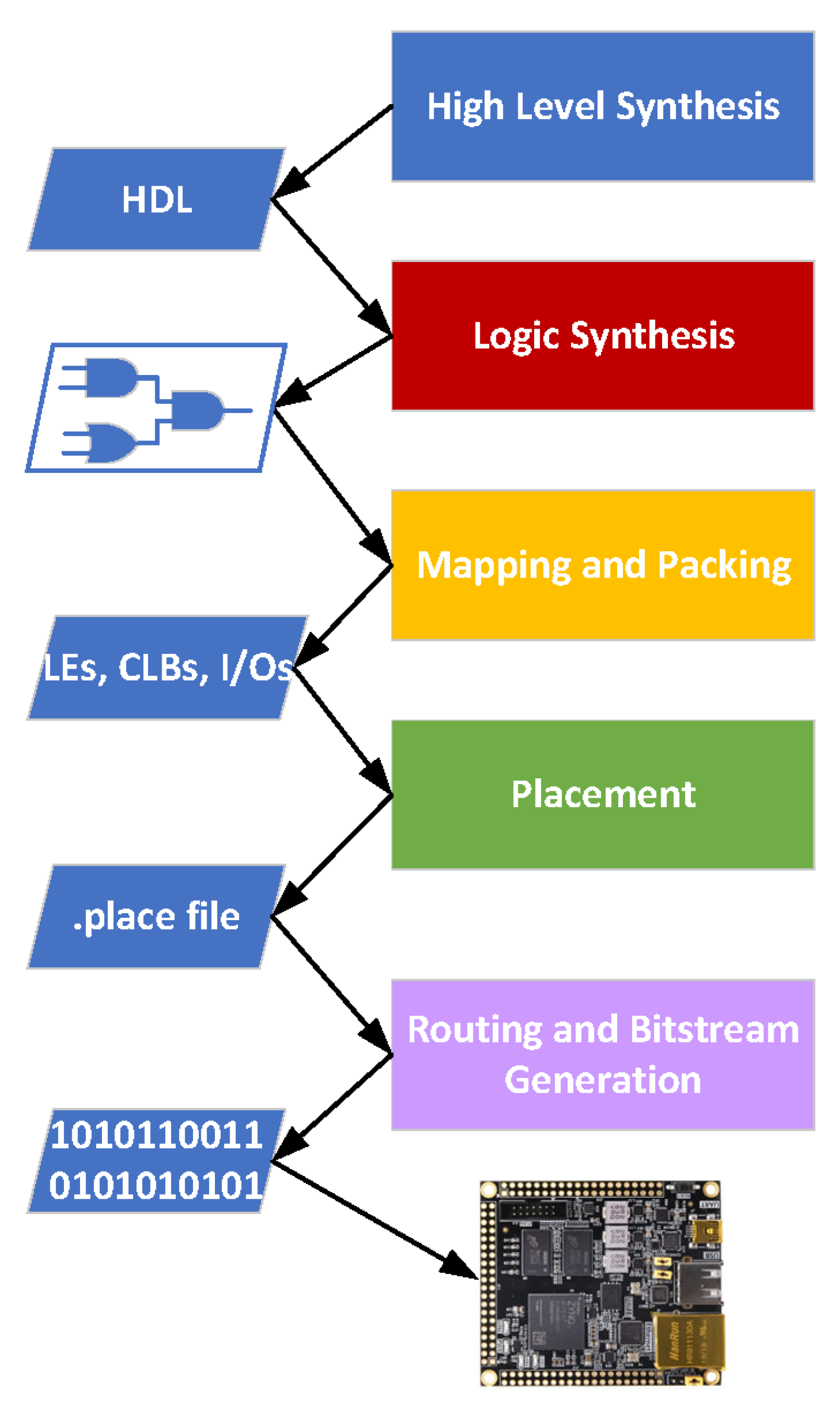
The effectiveness and quality of an FPGA architecture relies on the backend flow provided with an FPGA. Figure 2 provides an overview of conventional FPGA backend flow. It can be seen from this figure that the FPGA flow starts with the description of design in a high-level language and after passing through various complex steps, it ends with the bitstream generation of the design which is finally loaded onto FPGA. In this section, we summarize the important steps of the conventional FPGA backend, as they are instrumental to understand the following sections.

2.1. High-Level Synthesis

High-level synthesis (HLS) is usually the first step in the FPGA backend flow. This step translates from untimed behavioral description such as C/C++ based specifications to hardware description language such as Verilog/VHDL. A typical example of HLS process is shown in Figure 3. In accordance with a Cadence estimate of the effect of its own HLS product line, the HLS design automation tools designed for hardware verification have the potential to reduce design time and verification costs by 25–50%. Therefore, industry giants such as Synopsys, Mentor, Intel and Xilinx also have their own HLS design-automation packages [18,19], to troubleshoot power or timing problems, thereby improving productivity in customized hardware design. This automatic conversion from behavior to hardware description has the advantage of the design re-usability by generating micro-architectures of different characteristics simply by changing the synthesis options. HLS Design Space Exploration (DSE) is used to automatically set the different synthesis options to find a trade-off of Pareto-optimal designs—finding micro-architecture of specific power, performance and area. As the number of synthesis options increases, the design space exploration search space grows supralinearly. However, it is found that a large number of synthesis options combinations will not lead to a Pareto-optimal design [20], resulting in drastically reducing the search space. This calls for efficient design space exploration options. While the options of design space exploration lie beyond the topic of this study, the readers are encouraged to refer to [21] for a detailed survey summarizing the efforts in HLS design space exploration.

2.2. Logic Synthesis

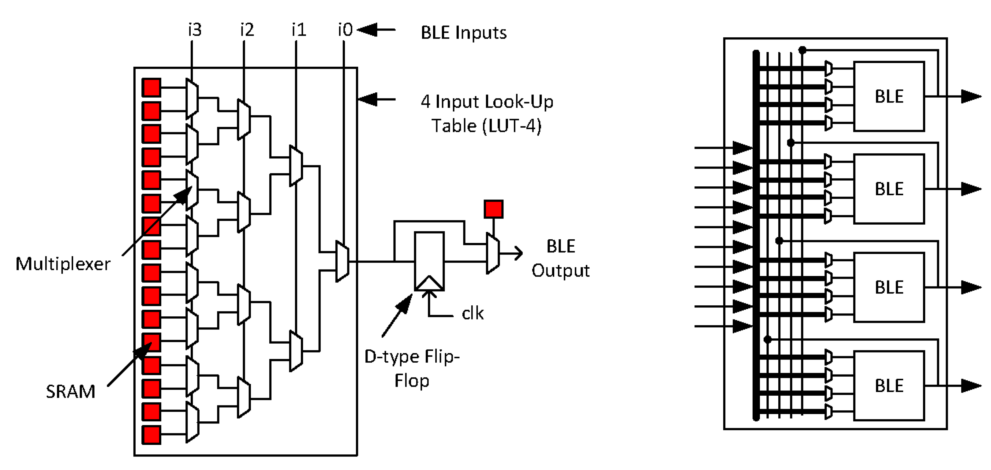
The logic synthesis [22] of the design to transform a hardware description language, such as verilog into Boolean gates, can be accomplished using numerous technology-independent techniques, with the ultimate objective of optimizing the Boolean network. The technology-dependent optimizations follow the logic synthesis, where Boolean network is transformed into a network of gates in the given set of blocks of the technology library. Traditionally, this transformation comprises of Look-Up Tables (LUTs) and Flip-Flops, considering different objective functions such as area and power. Heuristics such as Genetic algorithms have been employed to achieve this objective [23]. The FlowMap algorithm [24], and its later versions [25,26,27], is a popular traditional way of performing this FPGA technology mapping. Multiple versions cited above are known to optimize the parameters of depth, area and runtime of the Boolean network, ultimately resulting in the efficient mapping of a network comprising of I/Os, LUTs and Flip-Flops. The efficient mapping facilitates the network creation of I/Os and Configurable Logic Blocks (CLBs) in such a way that minimizes the inter cluster communication, with each cluster constituting the LUTs, Flip-Flops and other Basic Logic Elements. Opensourse frameworks such as Yosys [28] provide a basic set of synthesis algorithms, but have the limitation of accepting invalid code without reporting errors. Figure 4 shows the typical process of mapping and packing that is usually used in FPGA backend flow.

2.3. Placement

The next step in the FPGA backend flow, placement, is meant to optimize the routing resources when routing the connection between multiple connected blocks. Those connected blocks are placed near each other to further optimize the FPGA architecture by balancing the wire density. Traditionally, the placement algorithms are placed in one of the following three categories.

2.3.1. Partitioning-Based Approach

This approach is suitable for tree-based or hierarchical FPGA architectures. The netlist instances are distributed between clusters in such a way that merges highly connected instances within the same cluster. This results in the reduction of hyperedges that span more than one partition. Different heuristic algorithms [29,30] are developed to accomplish following objectives:
1.
Clustering, where hierarchy of clustered hypergraphs is formed by combining hypergraph vertices based on connectivity;
2.
Top-level partitioning, where the smallest hypergraph is partitioned using a fast initial solution generator and improved repeatedly by employing heuristics such as FM algorithm [29], and the process is repeated for the next smallest hypergraph;
3.
Refinement, where solutions are improved iteratively by projecting from smaller levels to the next.
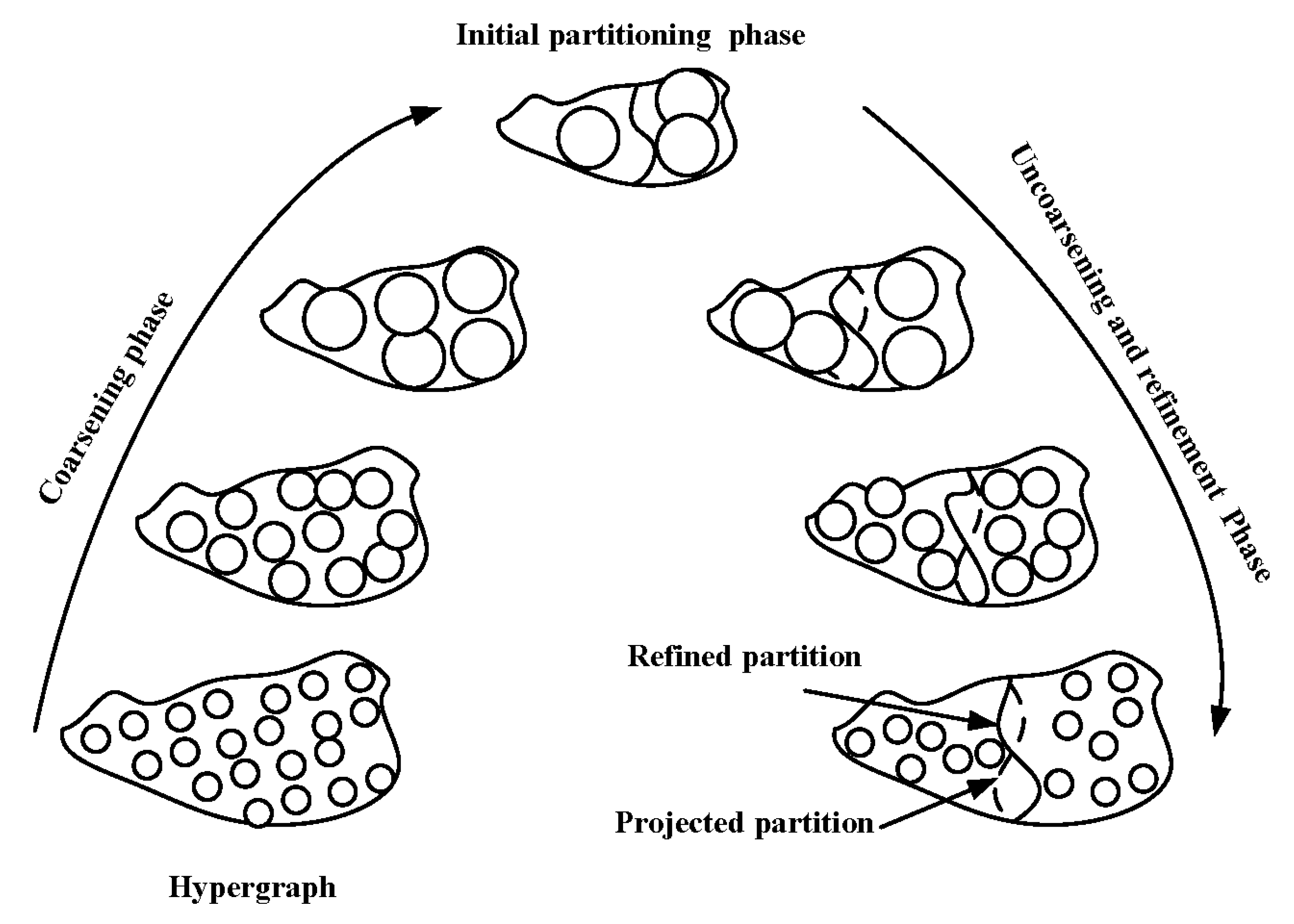
Figure 5 shows these steps where coarsening/clustering is followed by initial partitioning and refinement steps. Refinement algorithms allowing for high correlation between refined and initial hypergraphs are abundant in literature. These three steps ultimately result in reducing the number of overlaps iteratively, eventually producing a placement of logic blocks with legitimate possibility of the least overlaps. Several research efforts [31,32,33] have been made to improve the partitioning-based algorithms with the main aim to merge highly connected instances in the same cluster, thereby minimizing total interconnect length and maximizing the cut between two adjacent layers. For example, in [34], a partitioning-based algorithm is proposed that results in a decrease in power consumption, area and delay when compared with SA-based placement algorithm. This performance decline can be attributed to the cut size not being an exact function of wire length, timing or routability.

2.3.2. Analytical Placement Approach

This approach starts with the fixed placement of I/O objects, and then the logic block final placement is computed iteratively—much like partitioning-based approach—using a mathematical function to minimize the squared wire length. To this effect, this placement category is sometimes treated as a subset of partitioning-based approach. The mathematical objective function used is quadratic [35], which is an indirect measure of the wire length. The quadratic objective is followed by an iterative improvement technique, to optimize the results given by the quadratic function, as it does not link directly to the wire length. The Xilinx commercial placer uses this technique. The Analytical Placement approach is applied in the real-valued domain so its placement results need to be snapped onto the discrete placement slots on the FPGA grid.

2.3.3. Simulated Annealing Placement Approach

This placement approach is suitable for island style/mesh-based routing architectures and it uses a cost function to move the logic blocks to an optimized location in a limited amount of time. The cost function explores the solution space to optimize the run time. Traditionally, the optimization is accomplished by either of the two approaches: parallel move generation [36] and directed search of solution space [37]. Simulated Annealing (SA)-based placement is an extremely flexible approach and accommodates any objective such as wirelength of current placement [38] or speed performance. This is accomplished by assigning an objective function randomly that reflects the constraints meant to optimize, with weights assigned to each constraint according to its importance. The objective function is then optimized for the placement by random perturbations, and for each attempt, a change in cost, ΔC, is calculated. Each perturbation causes the logic block to move to a new location until the desired optimized placement is achieved. Perturbations can be either always accepted or accepted with a probability depending on the desired improvement in the objective function. The latter case is referred to as hill climbing, and it is important to accommodate although the corresponding perturbation worsens the cost function. There are occurrences when taking a few uphill steps that lead to the overall objective function optimization in the placement. As this technique is extremely flexible to accommodate any cost placement constraint, it is used in numerous popular CAD tools, such as Versatile Place and Route (VPR) [39,40]. Figure 6 shows the simulated annealing approach that uses wirelength as the optimization objective. Since SA is a metaheuristic approach itself, it holds a few challenges as well such as significant placement impact of the precision of numbers used in the objective function and the tuning of all the parameters resulting in multiple optimization points.

2.4. Routing

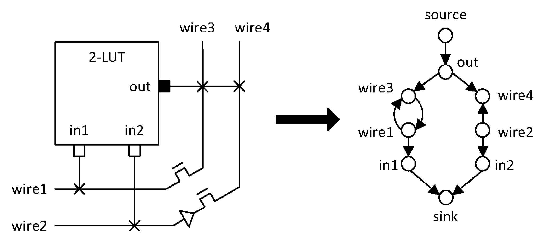
After the netlist instances are placed, connections are routed between them using the limited routing resources, with the objective of each signal using a unique routing resource. For this purpose, the resources of FPGA are represented as a directed graph and an example of this representation is shown in Figure 7. Since the FPGA routing resources are limited, routing is deemed to be the most time-consuming phase of the CAD Flow requiring days for the largest commercial designs. Traditionally PathFinder [41] routing algorithm is employed, which uses an iterative, negotiation-based approach to successfully route all the signals in a netlist. The first pass of the PathFider approach employs Dijkstra’s shortest path algorithm, and then subsequently, signals are made to negotiate for routing resources. This interprets to a single metal wire being shared by multiple different signals in the initial steps of routing, which are then detached progressively by a rip-up and re-route mechanism. This results in a conflict-free solution as the signals eventually find the less congested nodes to meet their objective. The optimality of the objective is verified via a binary search algorithm. The routing process comes to a halt when the resources are not improving any more, eventually producing a viable routing. Several variations of PathFinder have been proposed—in [42], Swartz enhanced the PathFinder by reducing the router’s search during runtime. We note that the two largest FPGAs vendors, Xilinx and Altera, both use variations of PathFinder in their commercial routers. PathFinder stochastic routing models [43] have also been proposed, however, such models rely on estimated probability of connection lengths, as opposed to having accurate information of connection geometry.
The routing information of the netlist is used to program the SRAM bits of Look Up Tables. This bitstream information for the netlist is programmed on the FPGA using a bitstream loader and finally, the bitstream generator reads the mapping, packing, placement and routing information.

3. CAD Flow for FPGAs: Machine Learning Perspective

Machine learning techniques have been applied in electronic design automation (EDA) since the 1990s [44], however, the recent exponential growth in semiconductor integrated circuits (IC) calls for a novel way of exploring the large design space with low latency. The tasks in each EDA step—design space exploration, simulation, verification and manufacturing preparation—can be modeled as an NP-complete problem, known to be tackled efficiently by modern machine learning techniques, as ML algorithms can manage large amounts of data quickly [1], thereby reaching the optimized state with minimum resource and time consumption. Such NP problems are common occurrences in EDA tasks, and several algorithms leading to the optimized state of EDA step being tackled have been proposed. Ryan proposes an algorithm, STAGE [45] that explores the design space of many core systems in two stages. Local search guided by a cost function, followed by meta search that exploits the search trajectories of local search to predict the outcome of a local search procedure from a given starting point. For lithography hot spot detection, Ding [46] uses SVM, whereas Yang [47] uses a deep CNN that targets representative feature learning. Both ML tools show promising results. Addressing topology selection, Matsuba [48] employs a deep CNN classifier to decide for the optimal topology from the circuit characteristics, with complete success for four registered topologies. Wang [49] addresses the device sizing by employing a multistep reinforcement learning framework that automatically optimizes the circuit parameters. Both the local and global status of the corresponding transistor is taken into account to outperform the random search, as well as Bayesian optimization and even human experts. The point insertion between two modules to observe the output of former module and control the input of later module is called point insertion problem, which plays a key role in verification by reducing test complexity. Ma [50] uses Graph Convolutional Network (GCN) for point insertion. The netlist is first mapped to a directed graph, then nodes are labeled as per their difficulty to observe, and finally, a GCN classifier is trained, resulting in a reduction of observation points by 11%.
The above-mentioned examples of EDA tasks being modeled as NP-complete problems and then applying the machine learning to reach the optimized state demonstrate that it is high time that we integrate the sophisticated machine learning paradigms into FPGA CAD design, which would result in a time-efficient and effective FPGA backend flow steps. This section reviews the little work that has been completed in that regard. We dedicate each subsection to the relevant CAD flow step, i.e., HLS, Logic Synthesis, Placement and Routing.

3.1. High-Level Synthesis Using Machine Learning

High-Level Synthesis (HLS) is seeing a renewed popularity, driven by its ability to evaluate efficiently the machine learning-based matrices. For example, Flex Logix has a neural network infrastructure around its eFPGA capabilities to tailor some units on the chip [51]. One of the objectives of ML algorithms in HLS is to estimate the performance results in terms of resource and time optimization. In that regard, Makrani [52] modeled the time optimization as a regression problem, and then used the deep learning training platform Minerva [53] to evaluate the clock frequency of the HLS tool’s output code. The flow used by [52] is also shown in Figure 8. The work was further improved by incorporating neural networks, SVM and random forests, to obtain HLS timing accuracy of 95%. Another application of machine learning in HLS is to explore the design space. There are certain efforts demonstrating that combining the ML algorithms with traditional heuristics such as SA overcomes the limitation of these heuristics of not being able to learn empirical information from the design to be explored. For example, Pingakshya [54] presents a machine learning-based HLS design space explorer that predicts very accurate results when combined with heuristics such as SA. Low-Level Virtual Machine (LLVM) is employed to generate the features which are then given as input to a regression algorithm. Schaefer [55] combines SA with decision trees to reduce the design space, thereby speeding up the design space exploration time, showing promising results. Machine learning techniques are likely to become more popular for HLS design, creating a good resource for chip makers in the design process. Already, a lot is happening in medical detection and telecommunications domains. Huawei, Qualcomm and other mobile chip companies are opening APIs on their phones to facilitate developers in HLS optimization [56].

3.2. Logic Synthesis

After the high-level software is synthesized into an HDL model, an HLS report is generated along the model to estimate the expected performance, resource usage and timing. This HLS report then undergoes logic synthesis. The report estimates are almost always inaccurate and can be improved significantly using ML-based algorithms. The report estimates almost always have deviations between measured and actual values. These inaccuracies can be improved significantly using ML-based algorithms, such as clustering methods proposed in [57] based on Fuzzy Logic. The proposed algorithms take into account the neighbor information to estimate the deviations beforehand with a significant estimation performance increase.
The authors of [58] use 87 features extracted from the HLS report to train a set of machine learning models—linear regression model, neural network and gradient tree boosting—that reduce the HLS estimation errors by up to 138%. For HLS, Dong [59] leverages an ML method inspired from Rival Penalized Competitive Learning (RPCL) to classify which designs need to be synthesized for a true Pareto-optimal solution, thereby reducing the design candidates that need to run through the downstream implementation flow. For accurate resource estimation in the HLS report, Koeplinger [60] proposes a three-layered Artificial Neural Network (ANN)-based framework that predicts resource usage from pre-characterized area models of a small set of architectural templates. A new parameterizable HDL is introduced that generates efficient FPGA designs automatically from a high-level description based on parallel patterns. Another challenge in FPGA synthesis is the slow timing of CAD runs, which could take days of runtime on modern designs. Yanghua [61] addresses this challenge of timing convergence by combining the predictions of multiple classification algorithms, which ultimately results in the improved predictive accuracy of InTime, which is an automated timing plugin for Xilinx and Altera CAD tools [62]. The classification algorithms used for improving timing convergence include logistic regression, random forest, SVM, and ANN. ML has been applied to autotune frameworks facilitating the large multi-scale space exploration of tool-specific parameters, critical during FPGA synthesis phase, and such efforts are funded by numerous organizations, including DARPA [63]. To predict an accurate mapping, Ustun [64] constructs and trains a Graph Neural Network (GNN) to infer the mapping choices about hardened blocks, with the ultimate objective of capturing the association between operations from the dataflow graph. A reduction in root mean square error (RMSE) by 72% was observed.
All these ML techniques are used to ensure that the FPGA Synthesis approximation is close to final prototyped design. Once this task is accomplished, the design is deemed to be technology-mapped and packed, as per the resource requirements of target FPGA, and is considered to be ready for the next steps of FPGA flow.

3.3. Placement

Placement is deemed to be one of the most time consuming steps in CAD flow and it aims to obtain an evaluation of two objectives: congestion estimation and routability prediction. As detailed in Section 2, the evaluation criteria are meant to achieve wire length and timing optimization. Several ML techniques have been used to achieve accurate congestion and routability evaluations. Elgammal [65] leverages traditional SA technique by proposing seven directed moves with a reinforcement learning agent controlling the proposed moves throughout the anneal, achieving 5% less wirelength and 1% critical path delay gains at high runtime budgets. Pui [66] proposes a probabilistic framework called RippleFPGA which can handle only single clock design, which is not pragmatic nowadays. He improves this shortcoming in [67] by proposing three supervised ML models with underlying processing achieved by SVM for clock-aware placement in modern heterogeneous FPGAs. However, the shorter training time combined with most data usage for training (70%) might result in overfitting. Additionally, the proposed congestion model only considers the congestion levels between SLICEs. In another work, an SVM-based Linear Regression model achieved 90% accuracy on FPGA Placement contest benchmark [68] when compared with the congestion estimates of Vivado Design Suite. However, when tested to predict real congestion, the accuracy dropped by a staggering 60%. The work was further improved and tested by Maarouf [69], achieving an accuracy of 85% and a runtime 291 times faster in a real-world congestion scenario, outperforming the other methods in terms of accuracy and runtime. Al-Hyari [15] further builds on [69] to propose MLCong, a nine-step congestion estimation framework that implements and compares placement prediction models: linear regression, K-Nearest Neighbor, ANN and Random Decision Forests, and a test on 360 benchmarks—ranging from 0.1 to 1.1 million gates—provided directly by Xilinx. The approach used by [15] is also shown in Figure 9. For this work, the random forest algorithm yielded the best results due to having the shortest testing time required. The proposed ML model reduced the average router runtimes by 19% compared with the global router, while accurately capturing the characteristics of congestion in the placed circuit. In an effort to obtain the correlation between congestion locations at global routing and cell placement, a deep learning CNN model, DLRoute [70], is proposed that determines whether it is possible to route a placement solution without the overhead of a conventional router. The output is a binary (True/False) label indicating whether the placement can be successfully routed. Despite achieving a high prediction accuracy (i.e., 96%) and the inference times in milliseconds, it has some shortcomings, such as requiring larger training sets, more training time, being computationally expensive and being less transparent than ML models. Martin [71] addresses these challenges by introducing the ensembles techniques that merge multiple ML techniques into a single predictive model, which outperforms DLRoute [70] in terms of accuracy, precision, sensitivity and specificity, thereby further improving the prediction accuracy.
With regards to ML-based routability prediction, Qi [72] proposes a regression technique global routing model that reduces design rule violation at the cost of runtime overhead. Zhou [16] proposes a detailed routability prediction model based on supervised learning. Multivariate adaptive regression is performed to train the connection between placement and detailed routing, achieving an average prediction accuracy of 79.8%. There are proposed algorithms using Fuzzy C-Means [57] that consider the constraint of neighbor information and have shown good performance on various types of images. The consideration of neighborhood information makes them an attractive candidate for proposing an effective placement strategy that would connect the blocks placed to each other, thereby optimizing the wire density. Building on such algorithms to come up with an optimized Placement strategy is yet another promising research direction.

3.4. Routing

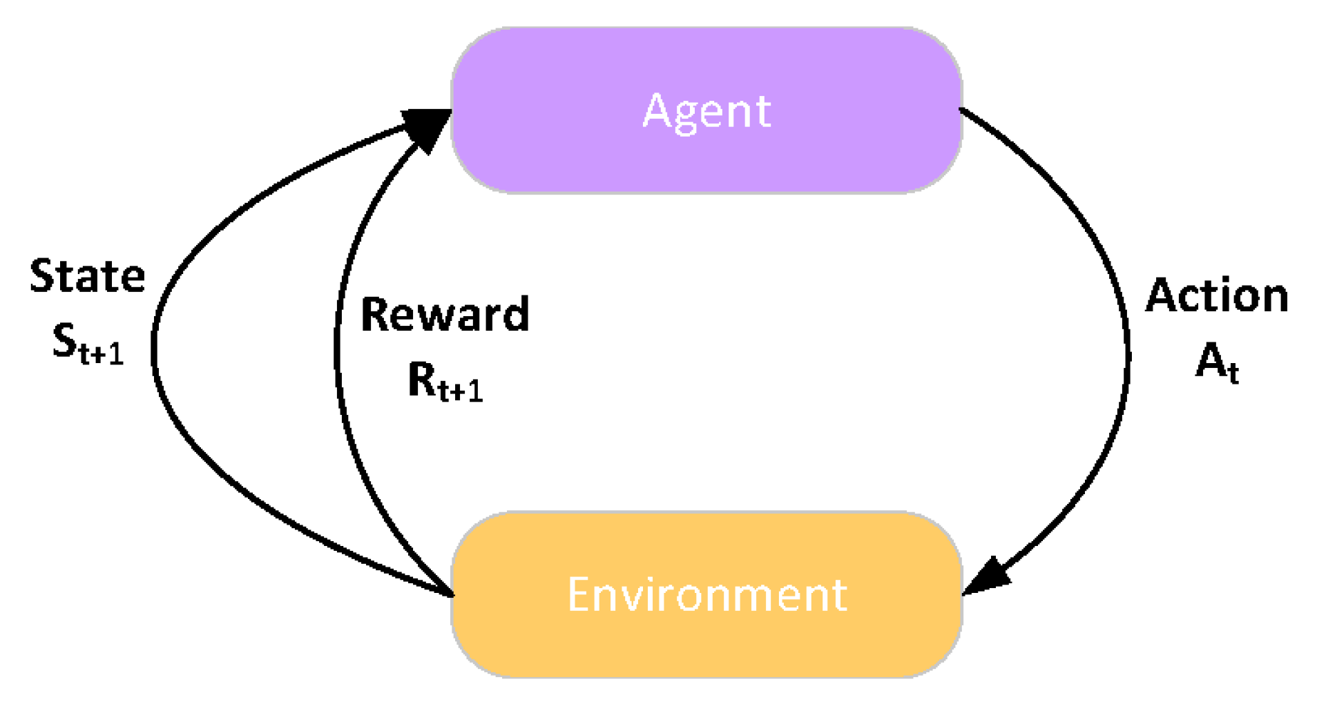
The placed netlist is the input to the routing step. The routing link and placed netlist can be modeled as a directed routing resource graph (RRG), thereby transforming the routing problem into finding the shortest path in a graph theory, which has been solved using several machine learning solutions [73,74]. However, very few of the proposed solutions to find the shortest path have been applied to the FPGA CAD routing paradigm, and they have their own sets of limitations. For example, the routing step has been formulated as a deep reinforcement learning problem by employing a Deep Q-network that conjointly routes the nets and the pins [75] in a simulated environment, which might not be scalable to the actual routing environment. Farooq [76] proposed a reinforcement learning-based solution to the routing problem by transforming the classical routing iterative process into the training process of reinforcement learning. While moving from one node to another, a reward (or penalty) is associated with the agent’s experience, which is taken into account for the subsequent moves. The reinforcement learning scenario is depicted in Figure 10. The results demonstrate a reduction in execution time by 30%. The work is further elaborated in [77] by experimenting with the parameter ϵ in the proposed ϵ -greedy approach. The ϵ value at 0.001 maintains a balance between a purely greedy and purely exploratory approach and helps in exploring the solution space more efficiently, as shown by the results on the two sets of open-source heterogeneous benchmarks used.
We have cited some work at the placement stage that predicts the routing congestion estimation, however, it is difficult to obtain a precise estimation of the routing information at the placement step. Despite routing being a time-consuming and important step in FPGA back-end flow, we have observed a dearth of machine learning solutions dedicated to the task. However, there are some efforts worth adapting. Jain [73] models routing in ICs as a binary segmentation problem and uses a CNN to classify pixels in each layout layer—eight in total—to be on or off. The encoded layouts containing spatial locations of pins to be routed are the inputs to the CNN. However, the usage of simplistic design rules to assess CNN learnability together with the testing on the authors’ own designed datasets does not give an accurate performance estimation of the approach. The authors of [74] model the circuit routing as a sequential decision-making problem to solve it by Monte Carlo tree search with deep neural network-guided rollout. Experiments on randomly generated single-layer circuits might not be reflective of the routing needs for today’s heterogeneous FPGAs. Another approach that can be exploited is formulating the routing problem into a classical image processing problem and tackling the problem by machine learning techniques. For example, Utyamishev [78] models the global routing problem as an imaging problem that autonomously routes unseen layouts using a deep learning system. Although there have been some efforts in utilizing machine learning algorithms to route the placed netlists in FPGA, the work is still in the preliminary phase and it requires significant effort from the research community. As the scale of FPGA circuits continues to increase, without machine learning mechanisms, the time requirement for efficient routing will also increase. Therefore, it is high time to explore machine learning-based solutions that could improve the routing efficiency.

4. Research Challenges and Opportunities

It is critical to integrate ML algorithms in CAD for FPGAs, as this would reduce the time to market by significantly improving the compiling time. Moreover, the ever-increasing demand for performance and energy efficiency for Industry 5.0 applications would require a dedicated effort towards the identified limitations in previous section. As we identify in Table 1, there are several gaps in employing machine learning techniques across FPGA CAD backend flow. This section is aimed at discussing the identified gaps in Table 1 that will eventually improve the existing state of the domain. We observe that the work cited in Section 3 has helped us identify the following six research opportunities:
  • Lack of open-source benchmarks;
  • Absence of machine learning-based complete backend flow;
  • Multi FPGA-prototyping using machine learning;
  • Domain-specific flow;
  • Federated learning for FPGAs;
  • Lack of explainability in ML-based flow.
Each of the identified opportunities represents a promising vision for the future research direction. Active pursuit of these challenges will address the bottlenecks associated with FPGA backend flow: inaccuracy, longer time to market, undesired manual intervention, to name a few. This in turn will make it possible to link things with each other and with people, as visualized in Industry 5.0 [1]. We explain each of these research opportunities next.

4.1. Lack of Open-Source Benchmarks

Standard benchmarking practices are critical in order to evaluate FPGA systems and determine their potential to support target applications. As evident from the previous section, the FPGA industry is expanding to support Industry 5.0 applications and machine learning and deep learning are at the core of it. The FPGA CAD metrics—logic capacity, performance speed, resource utilization, power consumption, area required for placing designs, etc.—only have meaning when measured using dedicated benchmarks. There is currently no existing opensource benchmark suite that consists of deep learning workloads. Therefore, the lack of machine learning benchmark circuits to measure the deep learning workloads is an important challenge. While MLSBench [79] was proposed recently, it covers high-level synthesis only, which is technology-independent step of FPGA CAD flow. The benchmarks relying on experimental flow, such as VTR [80] which maps the CAD flow to map suites of designs to the target FPGA architecture, are difficult to rely upon when evaluating FPGAs optimized for machine learning applications. This difficulty can be attributed to two reasons:
1.
Publicly available benchmarks such as Titan [80] lack the machine learning acceleration examples;
2.
Mapping algorithms in multiplication/addition operations in ML context requires significant functionality implementation and such mapping algorithms are not trivial to create, e.g., for AI tensor blocks [81] which require a great amount of multiplication/addition.
There have been some efforts to add dedicated ML blocks to the FPGA fabric to efficiently perform tensor operations. For example, Arora [82] proposes adding hardened blocks to perform tensor operations such as matrix multiplication or element-wise computations. Intel’s AI Tensor Blocks are arranged in columns as well. However, such efforts evaluate performance using a set of small matrix multiplication micro-benchmarks, written by hand to target the hardware, which are insufficient. Recently, Roorda [17] discussed the FPGA architectures in the context of deep neural networks and proposed a blueprint benchmark to address the lack of suitable benchmark circuits. However, the proposed blueprint benchmark has several limitations:
1.
Not all embedded blocks are represented;
2.
Not all aspects of deep neural network-based architecture are covered;
3.
Benchmark is highly dependent on assumptions about critical metrics such as timing delays and baseline architectures.

4.2. Machine Learning-Based Complete Backend Flow

As discussed in Section 3 of the paper, the work in [58] suggests a machine learning-based synthesis solution for FPGA backend flow. They report an improvement of 138% in performance and the results have greatly improved accuracy. Similarly, The authors of [65] present machine learning-based solutions for FPGA placement. The authors report a 5% improvement over conventional placement solutions in terms of wirelength and 1% improvement in terms of critical path delay, while significantly improving the runtime. They also report an accuracy of more than 85%. Additionally, the work in [76] uses a reinforcement learning-based solution to speed up the routing and find a solution in a short amount of time while not compromising the quality of solution. Optimization of the FPGA CAD tool for one specific step—packing—is discussed in [83]. It is evident from the work cited above that there exist individual solutions in the state of the art that provide machine learning-based solutions for individual steps of the backend flow of FPGAs. These solutions use a mixture of machine learning algorithms for different steps of FPGA backend flow. Some of these algorithms are random forest, SVM and reinforcement learning, among others. Although these solutions give good results for individual steps, they fail to provide complete experience of the entire FPGA end-to-end flow. A lot of work has been done in the conventional FPGA backend flow domain and there exist different flows that give an end-to-end experience to the user for conventional backend flow [84]. However, to the best of our knowledge, there is no FPGA backend flow that is based on machine learning algorithms and that gives a complete experience from synthesis to routing. As discussed in [84], having a complete flow is really important if we want to benefit from the efficiency of modern machine learning algorithms. Otherwise, the time and efficiency gain achieved in individual steps might be lost in moving from one tool to another, especially when each tool is provided by separate contributors. From our point of view, this is a big opportunity for researchers to devise a complete backend flow that provides an end-to-end experience and that can be used to significantly speed up the FPGA backend flow and do so without loosing the advantage of time and speed.

4.3. Multi-FPGA Prototyping Using Machine Learning

FPGAs were introduced to the consumer market a few years ago. Today, they are a multi-billion-dollar market. Among many applications of FPGAs is prototyping of complex Application-Specific Integrated Circuit (ASIC) applications. The prototype of an ASIC on FPGA requires a multi-FPGA platform and along comes the backend flow for multiple FPGAs. The steps for multi-FPGA prototyping are different from those of single FPGA backend flow. They involve different algorithms and optimization objectives. For example, a multi-FPGA prototyping flow requires inter-FPGA partitioning [85] whose main objective is to minimize the cut-net count between different FPGAs. Similarly, the routing problem for multi-FPGA prototyping is rather based on finding a feasible solution for tracks between the FPGAs rather than finding a solution for intra-FPGA routing. There is significant work that has been dedicated to multi-FPGA prototyping backend flow. However, all of it is oerformed using conventional algorithms. For example, for partitioning, usually, a min-cut-based partitioning approach is used [85]. For routing, usually, a negotiated congestion-driven-based routing approach is used [86]. None of the existing solutions use a machine learning-based approach for the backend flow of multi-FPGA prototyping platforms. The backend flow of multi FPGA prototyping requires a considerable amount of time. That time can be minimized by incorporating machine learning algorithms in multi-FPGA prototyping platforms and this could be a big research opportunity for researchers working in the FPGA backend flow domain.

4.4. Domain-Specific Flow

FPGA could be an efficient candidate solution for the implementation of domain-specific accelerators such as Google’s TensorFlow. The availability of FPGAs in the public clouds—Amazon AWS F1 [19] and Nimbix [87]—has made it possible to create a customized application specific domain-specific accelerator. However, the unavailability of dedicated FPGAs on-premise is a barrier that can be addressed by a domain-specific backend flow. The backend flow should be tailored to the dedicated application, e.g., computer vision, speech recognition, facial expression identification, image processing, natural language processing, autonomous driving, etc., and the design of application-specific backend flow will be a critical step towards the customized computing application design on the programmable fabric of FPGA. For example, for autonomous vehicles requiring quick and rational decision making, deep neural networks-based architecture seems to be the logical choice. In the case of deep neural networks comprising of several layers, the FPGA processing units should be placed as close to the training/testing data as possible. In existing CAD tools, each application needs to achieve a dedicated design closure that requires manual intervention in calibrating and configuring a large set of design parameters to achieve the desired QoS. This manual effort in the existing CAD tools could require days for larger circuits. On the contrary, the machine learning techniques used in multiple CAD flow steps, reviewed in Section 3, are employed to achieve the results in an intelligent self-guided way. This discrepancy is a major challenge requiring more research effort, and holds promise for the domain-specific FPGA design while maintaining the reconfigurability.

4.5. Federated Learning for FPGA

The massive personalized data of Industry 5.0 applications implemented on SoC need to be secured as it might contain sensitive information, pertaining to personal finances or health. It has been demonstrated recently that both commercial and open-source FPGA CAD tools are susceptible to various attacks. For example, authors in [88] demonstrate how the original logic function can be tampered in Xilinx ISE. While introducing machine learning algorithms in the FGPA backend flow, we are indirectly integrating the third-party IP cores and data-analysis software, thereby compromising on the trustworthiness of CAD tools. Federated learning-based [89] methods have the potential to overcome such security challenges as they take a decentralized approach to train the model for appropriate CAD flow step, without anyone seeing or touching the complete training data set. This could address the privacy and security concerns. However, federated learning comes at the cost of increased computational complexity, which is exacerbated in the case of heterogeneous platforms like FPGA. The increased computational cost is attributed to the usage of algorithms such as FedAvg [89] to process the cryptographic and aggregation security features inherent in federated learning. Recent studies show that while federated learning is efficient for one specific algorithm [90], more research is required to address the limitation of using federated learning for variable and flexible circuits, to make the most of the reconfigurability associated with FPGAs. One such research effort is Microsoft’s Project Brainwave [91] which is a high-performance distributed system rendered with Intel’s Stratix FPGAs that use low-latency artificial intelligence algorithms. Another important federated learning limitation that would require more focus is end-to-end training speed of machine learning-based CAD algorithms, as model parameters are shared between multiple participating nodes to keep the training data private. There is also a paradox associated with federated learning-based methods. Despite their successful applications towards users’ privacy, they introduce privacy challenges of their own. For example, a malicious user can infer the FPGA’s training algorithm from the local learning model during the communication with aggregation server, which could result in longer convergence time of the employed CAD algorithm.

4.6. Lack of Explainability in ML-Based Flow

Section 3 provided a detailed discussion on the role of machine learning algorithms in the FPGA backend flow. The studies cited in that section indicate that different machine learning algorithms give efficient results for different steps of FPGA CAD flow. For example, for HLS, SVM and random forest algorithms give good results, for logic synthesis, the use of GNN is a good choice and for placement and routing SVM, KNN and RL algorithms give good results. It is important to note here that a single machine learning algorithm does not always give the optimal results for every step of the FPGA CAD flow. Moreover, it is also interesting to note that the authors od those studies present the results, however, the discussion behind the comparison of why one algorithm is better than the other is usually missing.
This is mainly because of the complex nature of machine learning algorithms and as the complexity of the algorithms grows, it becomes more difficult to explain or reconstruct the underlying thought process [92]. Some of the most complex algorithms are so complicated that even the engineers or researchers who designed them cannot explain how these algorithms arrive at their conclusions. Under such circumstances, it is very important to add some explainability to the ’black box’ nature of machine learning algorithms. This will make the conclusions derived from an algorithm more understandable and add greater explanation to their intended uses and possible biases. In this regard, some work has been presented in explainable artificial intelligence (XAI) [93,94]. However, no work is available on explainable machine learning from a FPGA CAD perspective. The goal of explainable ML would be to add some reasoning to the findings and conclusion of machine learning algorithms that are being used for FPGA backend flow. This transparency would render the backend flow behavior more comprehensible and reliable for the end users and engineers who use backend flow on a daily basis to implement new applications on FPGAs.

5. Discussion

The breakthroughs in the development of modern ML algorithms have provided a significant opportunity to optimize the CAD flow process and maximize the value from FPGA-based prototyping, which is an important step in the pre-silicon validation of next-generation SoCs. However, each target SoC possesses unique needs and requires a wide variety of chip designs being prototyped, with massive data processing requirement. The reprogrammable nature of FPGA together with custom parallelism guarantees the flexibility and variety required in the chip designs. The extensive data processing required can be addressed by novel types of CAD platforms such as CAD as Adaptive OpenPlatform Service (CAOS) [95], which heavily automates the development flow steps, while ensuring usability, modularity and interactivity—three essential features to run and compute intensive ML algorithms. The framework is hosted by novel architectures that provide a complete integrated development experience, while accelerating an application on reconfigurable hardware. CAOS is conceived to provide interfaces that could enhance the functionalities and services that result in adapting reconfigurable hardware in hard processor system (HPS). Such functionalities could include Acceleration-as-a-Service, which will enable the CAD developers to materialize the end-user requirements of greater application performance by exploiting new computationally intensive applications that would otherwise be unfeasible or impractical. The FPGA manufacturing giants are already working with industry partners to implement the cloud-based FPGAs for Industry 5.0 applications requiring compute intensive SoCs. For example, Intel collaboration with Alibaba Cloud offers two popular software development flows, RTL and OpenCL, to developers using FPGA-based accelerator capabilities, as they work on large and intense computing workloads [96]. The SDAccel is a Xilinx environment that eases the process of accelerating compute intensive algorithm employing sophisticated ML algorithms using FPGAs. The algorithm design is optimized before downloading and running the design on acceleration boards, thereby making it a viable choice for developers targeting FPGA-as-a-Service offerings. The SDAccel environment offers tools and reports to analyze the host application’s performance and identify potential areas for acceleration. In order to monitor hardware performance in real time, the SDAccel tools also offer automated runtime instrumentation of cache, memory and bus utilization. The same environment is used to create and run the algorithms on the available FPGAs in Amazon Web Services (AWS) EC2 F1, which is one of the first attempts to introduce high-performance reconfigurable computing systems to the cloud [97]. In addition to a runtime based on the OpenCL APIs that may be used by the host-side software to communicate with the accelerator, SDAccel offers the user a toolchain for programming and optimizing the application on Xilinx FPGAs using a high-level language (C, C++ or OpenCL). The cloud-based development environments, such as Alibaba clouds [97], have testing benchmarks, such as Vivado, that the CAD user can benefit from, while emulating and simulating the target design, comprising deep learning algorithms for computing-intensive designs requiring data encryption, video compression, hardware emulation, etc.
Figure 11 depicts the high-level architecture where the SoC applications for farming, healthcare, FinTech, transport, drones, etc., could be developed at a higher abstraction level, without worrying about the memory or other resource requirements. Despite being a relatively new idea, we believe that this is a promising research spot that requires more effort by the researchers in developing such cloud-based environments, so that they can be an efficient solution of the research challenges discussed in Section 4. The dedicated areas that will ease the path towards a smoother FPGA-as-a-Service (FaaS) will include development of open-source benchmarks optimized for ML algorithms, an end-to-end-consistent experience that covers all the steps of CAD flow, multi-FPGA prototyping tools with the objective of intra FPGA optimization, engineering domain-specific accelerators available on-premise and in-cloud for dedicated application development, engineering explainable ML algorithms dedicated to CAD backend flow, and federated learning incorporation within the development process to ensure data security. Currently, handcrafted solutions created by skilled designers outperform implementations created by the automated cloud-based frameworks such as CAOS. However, moving forward, with the advent of computationally expensive ML algorithms, the big data processing volume will restrict human involvement in CAD flow steps decision making, while these algorithmic decisions will be used in the SoC applications, which are becoming more and more consequential to society. For example, the United Nations Sustainable Development Goals [98] mention Industry, Innovation and Infrastructure, and SoCs are the basic building block of the all innovative infrastructure, be it healthcare devices, sophisticated farming equipment or a smart building constructed via 3D printing. The timeline to meet the SDG by 2030 indicates that the modern trends identified in this work within FPGA CAD flow are a major research opportunity for the international chip manufacturing industry that holds the promise of actualizing Industrial Revolution 5.0.

6. Conclusions and Future Work

The backend flow of FPGAs involves complicated and time-consuming steps and the performance of the final design greatly depends upon the quality of the tools and the experience and expertise of the designer using those tools. Recently, machine learning algorithms have found their way into almost all stages of the FPGA backend flow. The main objective of these algorithms is to minimize the implementation time without compromising the quality of the final design and at the same time decrease dependence on the design engineers. In this paper, we provide a comprehensive review of various machine learning techniques and their usage at different stages of the FPGA backend flow. The review of state-of-the-art work suggests that incorporation of machine learning algorithms such as random forest, SVM, CNN, RL, etc., has greatly improved the implementation time without compromising the quality of the design.
However, the usage of machine learning algorithms in the FPGA backend flow is still in its infancy and a lot needs to be done. For example, most of the studies reviewed in this paper use only a small set of benchmarks which is not available as an open-source resource for academic research purposes. To rapidly advance research in this domain, it is important to have a set of open-source and complicated benchmarks just like the conventional CAD flow of FPGAs. Moreover, different studies address only a particular stage of the backend flow and an end-to-end flow employing machine learning techniques from HLS to routing does not exist. Furthermore, the complex nature of machine learning techniques often renders the results produced through them inexplicable. This limits their application in a particular domain and a lot of work is required to make them vastly usable in EDA in general and FPGA CAD flow in particular. The cloud-based solutions, e.g., CAOS, seem promising and require further exploration in the framework of the challenges discussed in this work. In order to address the gaps in FPGA backend flow, the research community needs to focus more on the aforementioned challenges and opportunities.

Author Contributions

Conceptualization, I.T. and U.F.; methodology, I.T. and U.F.; formal analysis, I.T. and U.F.; investigation, I.T. and U.F.; resources, I.T.; data curation, U.F.; writing—original draft preparation, I.T. and U.F.; writing—review and editing, I.T. and U.F. All authors have read and agreed to the published version of the manuscript.

Funding

This research work was supported by Zayed University Research Start Up Fund # R22141.

Conflicts of Interest

The authors declare no conflict of interest.

References

  1. Taj, I.; Zaman, N. Towards Industrial Revolution 5.0 and Explainable Artificial Intelligence: Challenges and Opportunities. Int. J. Comput. Digit. Syst. 2022, 12, 295–320. [Google Scholar] [CrossRef] [PubMed]
  2. Available online: https://www.electronicsweekly.com/blogs/mannerisms/markets/auto-iot-will-drive-ic-market-says-ic-insights-2017-12/ (accessed on 2 February 2023).
  3. Stratix. 2022. Available online: https://www.intel.co.uk/content/www/uk/en/products/details/fpga/stratix/10.html (accessed on 7 December 2022).
  4. Chen, S.C.; Chang, Y.W. FPGA placement and routing. In Proceedings of the 2017 IEEE/ACM International Conference on Computer-Aided Design (ICCAD), Irvine, CA, USA, 13–16 November 2017; pp. 914–921. [Google Scholar]
  5. Zhuo, C.; Yu, B.; Gao, D. Accelerating chip design with machine learning: From pre-silicon to post-silicon. In Proceedings of the 2017 30th IEEE International System-on-Chip Conference (SOCC), Munich, Germany, 5–8 September 2017; pp. 227–232. [Google Scholar]
  6. Wang, Z.; Schafer, B.C. Machine leaming to set meta-heuristic specific parameters for high-level synthesis design space exploration. In Proceedings of the 2020 57th ACM/IEEE Design Automation Conference (DAC), San Francisco, CA, USA, 20–24 July 2020; pp. 1–6. [Google Scholar]
  7. Liaw, A.; Wiener, M. Classification and regression by randomForest. R News 2002, 2, 18–22. [Google Scholar]
  8. Fix, E.; Hodges, J.L. Discriminatory analysis. Nonparametric discrimination: Consistency properties. Int. Stat. Rev./Rev. Int. Stat. 1989, 57, 238–247. [Google Scholar] [CrossRef]
  9. Ward, S.; Ding, D.; Pan, D.Z. PADE: A high-performance placer with automatic datapath extraction and evaluation through high-dimensional data learning. In Proceedings of the DAC Design Automation Conference 2012, San Francisco, CA, USA, 3–7 June 2012; pp. 756–761. [Google Scholar]
  10. Chan, W.T.J.; Du, Y.; Kahng, A.B.; Nath, S.; Samadi, K. BEOL stack-aware routability prediction from placement using data mining techniques. In Proceedings of the 2016 IEEE 34th International Conference on Computer Design (ICCD), Scottsdale, AZ, USA, 2–5 October 2016; pp. 41–48. [Google Scholar]
  11. Tang, Y.; Zhang, L.; Bao, G.; Ren, F.; Pedrycz, W. Symmetric implicational algorithm derived from intuitionistic fuzzy entropy. Iran. J. Fuzzy Syst. 2022, 19, 27–44. [Google Scholar]
  12. Chhabria, V.A.; Kahng, A.B.; Kim, M.; Mallappa, U.; Sapatnekar, S.S.; Xu, B. Template-based PDN synthesis in floorplan and placement using classifier and CNN techniques. In Proceedings of the 2020 25th Asia and South Pacific Design Automation Conference (ASP-DAC), Beijing, China, 13–16 January 2020; pp. 44–49. [Google Scholar]
  13. Al-Hyari, A.; Areibi, S. Design space exploration of convolutional neural networks based on evolutionary algorithms. J. Comput. Vis. Imaging Syst. 2017, 3. [Google Scholar] [CrossRef]
  14. Chen, T.; Guestrin, C. Xgboost: A scalable tree boosting system. In Proceedings of the 22nd ACM Sigkdd International Conference on Knowledge Discovery and Data Mining, San Francisco, CA, USA, 13–17 August 2016; pp. 785–794. [Google Scholar]
  15. Al-Hyari, A.; Abuowaimer, Z.; Martin, T.; Gréwal, G.; Areibi, S.; Vannelli, A. Novel Congestion-estimation and Routability-prediction Methods based on Machine Learning for Modern FPGAs. ACM Trans. Reconfigurable Technol. Syst. (TRETS) 2019, 12, 1–25. [Google Scholar] [CrossRef]
  16. Zhou, Q.; Wang, X.; Qi, Z.; Chen, Z.; Zhou, Q.; Cai, Y. An accurate detailed routing routability prediction model in placement. In Proceedings of the 2015 6th Asia Symposium on Quality Electronic Design (ASQED), Kula Lumpur, Malaysia, 4–5 August 2015; pp. 119–122. [Google Scholar]
  17. Roorda, E.; Rasoulinezhad, S.; Leong, P.H.; Wilton, S.J. FPGA architecture exploration for DNN acceleration. ACM Trans. Reconfigurable Technol. Syst. (TRETS) 2022, 15, 1–37. [Google Scholar]
  18. Platforms, X.V. 2022. Available online: https://www.xilinx.com/products/design-tools/vitis/vitis-platform.html (accessed on 9 December 2022).
  19. EC2, A. 2022. Available online: https://aws.amazon.com/ec2/instance-types/f1/ (accessed on 9 December 2022).
  20. Wang, Z.; Schafer, B.C. Learning from the Past: Efficient High-level Synthesis Design Space Exploration for FPGAs. ACM Trans. Des. Autom. Electron. Syst. (TODAES) 2022, 27, 1–23. [Google Scholar] [CrossRef]
  21. Schafer, B.C.; Wang, Z. High-level synthesis design space exploration: Past, present, and future. IEEE Trans. Comput.-Aided Des. Integr. Circuits Syst. 2019, 39, 2628–2639. [Google Scholar] [CrossRef]
  22. Brayton, R.K. The decomposition and factorization of Boolean expressions. In Proceedings of the International Symposium on Circuits and Systems (ISCAS 82), Rome, Italy, 10–12 May 1982. [Google Scholar]
  23. Reyes Fernandez de Bulnes, D.; Maldonado, Y.; Trujillo, L. Development of multiobjective high-level synthesis for fpgas. Sci. Program. 2020, 2020. [Google Scholar] [CrossRef]
  24. Cong, J.; Ding, Y. FlowMap: An optimal technology mapping algorithm for delay optimization in lookup-table based FPGA designs. IEEE Trans. Comput.-Aided Des. Integr. Circuits Syst. 1994, 13, 1–12. [Google Scholar]
  25. Cong, J.; Ding, Y. On area/depth trade-off in LUT-based FPGA technology mapping. In Proceedings of the 30th International Design Automation Conference, Dallas, TX, USA, 14–18 June 1993; pp. 213–218. [Google Scholar]
  26. Cong, J.; Hwang, Y.Y. Simultaneous depth and area minimization in LUT-based FPGA mapping. In Proceedings of the Third International ACM Symposium on Field-Programmable Gate Arrays, Monterey, CA, USA, 12–14 February 1995; pp. 68–74. [Google Scholar]
  27. Cong, J.; Hwang, Y.Y. Structural gate decomposition for depth-optimal technology mapping in LUT-based FPGA designs. ACM Trans. Des. Autom. Electron. Syst. (TODAES) 2000, 5, 193–225. [Google Scholar] [CrossRef]
  28. Shah, D.; Hung, E.; Wolf, C.; Bazanski, S.; Gisselquist, D.; Milanovic, M. Yosys+ nextpnr: An open source framework from verilog to bitstream for commercial fpgas. In Proceedings of the 2019 IEEE 27th Annual International Symposium on Field-Programmable Custom Computing Machines (FCCM), San Diego, CA, USA, 28 April–1 May 2019; pp. 1–4. [Google Scholar]
  29. Fiduccia, C.M.; Mattheyses, R.M. A linear-time heuristic for improving network partitions. In Papers on Twenty-Five Years of Electronic Design Automation; ACM: Las Vegas, NV, USA, 1988; pp. 241–247. [Google Scholar]
  30. Bui, T.N.; Chaudhuri, S.; Leighton, F.T.; Sipser, M. Graph bisection algorithms with good average case behavior. Combinatorica 1987, 7, 171–191. [Google Scholar] [CrossRef]
  31. Ababei, C.; Feng, Y.; Goplen, B.; Mogal, H.; Zhang, T.; Bazargan, K.; Sapatnekar, S. Placement and routing in 3D integrated circuits. IEEE Des. Test Comput. 2005, 22, 520–531. [Google Scholar] [CrossRef] [Green Version]
  32. Das, S.; Fan, A.; Chen, K.N.; Tan, C.S.; Checka, N.; Reif, R. Technology, performance, and computer-aided design of three-dimensional integrated circuits. In Proceedings of the 2004 International Symposium on Physical Design, Phoenix, AZ, USA, 18–21 April 2004; pp. 108–115. [Google Scholar]
  33. Bartzas, K.S.A.; Soudris, D. Architecture level exploration of alternative schmes targeting 3d fpgas: A software supported methodology. Int. J. Reconfigurable Comput. 2008, 2008. [Google Scholar] [CrossRef]
  34. Chtourou, S.; Abid, M.; Marrakchi, Z.; Amouri, E.; Mehrez, H. On exploiting partitioning-based placement approach for performances improvement of 3d fpga. In Proceedings of the 2017 International Conference on High Performance Computing & Simulation (HPCS), Genoa, Italy, 17–21 July 2017; pp. 572–579. [Google Scholar]
  35. Kleinhans, J.M.; Sigl, G.; Johannes, F.M.; Antreich, K.J. GORDIAN: VLSI placement by quadratic programming and slicing optimization. IEEE Trans. Comput.-Aided Des. Integr. Circuits Syst. 1991, 10, 356–365. [Google Scholar] [CrossRef]
  36. Ludwin, A.; Betz, V.; Padalia, K. High-quality, deterministic parallel placement for FPGAs on commodity hardware. In Proceedings of the 16th International ACM/SIGDA Symposium on Field Programmable Gate Arrays, Monterey, CA, USA, 24–26 February 2008; pp. 14–23. [Google Scholar]
  37. Vorwerk, K.; Kennings, A.; Greene, J.W. Improving simulated annealing-based FPGA placement with directed moves. IEEE Trans. Comput.-Aided Des. Integr. Circuits Syst. 2009, 28, 179–192. [Google Scholar] [CrossRef]
  38. Marquardt, A.; Betz, V.; Rose, J. Using cluster-based logic blocks and timing-driven packing to improve FPGA speed and density. In Proceedings of the 1999 ACM/SIGDA Seventh International Symposium on Field Programmable Gate Arrays, Monterey, CA, USA, 21–23 February 1999; pp. 37–46. [Google Scholar]
  39. Betz, V.; Rose, J. VPR: A new packing, placement and routing tool for FPGA research. In Proceedings of the International Workshop on Field Programmable Logic and Applications, London, UK, 20 August 1997; pp. 213–222. [Google Scholar]
  40. Marquardt, A.; Betz, V.; Rose, J. Timing-driven placement for FPGAs. In Proceedings of the 2000 ACM/SIGDA Eighth International Symposium on Field Programmable Gate Arrays, Monterey, CA, USA, 10–11 February 2000; pp. 203–213. [Google Scholar]
  41. McMurchie, L.; Ebeling, C. PathFinder: A negotiation-based performance-driven router for FPGAs. In Proceedings of the 1995 ACM Third International Symposium on Field-Programmable Gate Arrays, Monterey, CA, USA, 12–14 February 1995; pp. 111–117. [Google Scholar]
  42. Swartz, J.S.; Betz, V.; Rose, J. A fast routability-driven router for FPGAs. In Proceedings of the 1998 ACM/SIGDA Sixth International Symposium on Field Programmable Gate Arrays, Monterey, CA, USA, 22–25 February 1998; pp. 140–149. [Google Scholar]
  43. Lou, J.; Krishnamoorthy, S.; Sheng, H.S. Estimating routing congestion using probabilistic analysis. In Proceedings of the 2001 international symposium on Physical design, Sonoma, CA, USA, 1–4 April 2001; pp. 112–117. [Google Scholar]
  44. Chavez, J.; Torralba, A.; Franquelo, L.G. A fuzzy-logic based tool for topology selection in analog synthesis. In Proceedings of the IEEE International Symposium on Circuits and Systems-ISCAS’94, London, UK, 30 May–2 June 1994; Volume 1, pp. 367–370. [Google Scholar]
  45. Kim, R.G.; Doppa, J.R.; Pande, P.P. Machine learning for design space exploration and optimization of manycore systems. In Proceedings of the 2018 IEEE/ACM International Conference on Computer-Aided Design (ICCAD), San Diego, CA, USA, 5–8 November 2018; pp. 1–6. [Google Scholar]
  46. Ding, D.; Gao, J.R.; Yuan, K.; Pan, D.Z. AENEID: A generic lithography-friendly detailed router based on post-RET data learning and hotspot detection. In Proceedings of the 48th Design Automation Conference, San Diego, CA, USA, 5–10 June 2011; pp. 795–800. [Google Scholar]
  47. Yang, H.; Luo, L.; Su, J.; Lin, C.; Yu, B. Imbalance aware lithography hotspot detection: A deep learning approach. J. Micro/Nanolithography MEMS MOEMS 2017, 16, 033504. [Google Scholar] [CrossRef]
  48. Matsuba, T.; Takai, N.; Fukuda, M.; Kubo, Y. Inference of suitable for required specification analog circuit topology using deep learning. In Proceedings of the 2018 International Symposium on Intelligent Signal Processing and Communication Systems (ISPACS), Ishigaki, Okinawa, Japan, 27–30 November 2018; pp. 131–134. [Google Scholar]
  49. Wang, H.; Yang, J.; Lee, H.S.; Han, S. Learning to design circuits. arXiv 2018, arXiv:1812.02734. [Google Scholar]
  50. Ma, Y.; Ren, H.; Khailany, B.; Sikka, H.; Luo, L.; Natarajan, K.; Yu, B. High performance graph convolutional networks with applications in testability analysis. In Proceedings of the 56th Annual Design Automation Conference 2019, Las Vegas, NV, USA, 2–6 June 2019; pp. 1–6. [Google Scholar]
  51. Available online: https://semiengineering.com/entities/flex-logix-technologies-inc/ (accessed on 9 December 2022).
  52. Makrani, H.M.; Farahmand, F.; Sayadi, H.; Bondi, S.; Dinakarrao, S.M.P.; Homayoun, H.; Rafatirad, S. Pyramid: Machine learning framework to estimate the optimal timing and resource usage of a high-level synthesis design. In Proceedings of the 2019 29th International Conference on Field Programmable Logic and Applications (FPL), Barcelona, Spain, 8–12 September 2019; pp. 397–403. [Google Scholar]
  53. Farahmand, F.; Ferozpuri, A.; Diehl, W.; Gaj, K. Minerva: Automated hardware optimization tool. In Proceedings of the 2017 International Conference on ReConFigurable Computing and FPGAs (ReConFig), Cancun, Mexico, 4–6 December 2017; pp. 1–8. [Google Scholar]
  54. Goswami, P.; Schaefer, B.C.; Bhatia, D. Machine learning based fast and accurate High Level Synthesis design space exploration: From graph to synthesis. Integration 2023, 88, 116–124. [Google Scholar] [CrossRef]
  55. Mahapatra, A.; Schafer, B.C. Machine-learning based simulated annealer method for high level synthesis design space exploration. In Proceedings of the 2014 Electronic System Level Synthesis Conference (ESLsyn), San Francisco, CA, USA, 10–11 June 2015; pp. 1–6. [Google Scholar]
  56. Available online: https://support.huawei.com/enterprise/en/doc/EDOC1100116632/4988e57/ops-apis-supported-by-a-device (accessed on 9 December 2022).
  57. Zhang, Y.; Bai, X.; Fan, R.; Wang, Z. Deviation-sparse fuzzy c-means with neighbor information constraint. IEEE Trans. Fuzzy Syst. 2018, 27, 185–199. [Google Scholar] [CrossRef]
  58. Dai, S.; Zhou, Y.; Zhang, H.; Ustun, E.; Young, E.F.; Zhang, Z. Fast and accurate estimation of quality of results in high-level synthesis with machine learning. In Proceedings of the 2018 IEEE 26th Annual International Symposium on Field-Programmable Custom Computing Machines (FCCM), Boulder, CO, USA, 29 April–1 May 2018; pp. 129–132. [Google Scholar]
  59. Liu, D.; Schafer, B.C. Efficient and reliable high-level synthesis design space explorer for FPGAs. In Proceedings of the 2016 26th International Conference on Field Programmable Logic and Applications (FPL), Lausanne, Switzerland, 29 August–2 September 2016; pp. 1–8. [Google Scholar]
  60. Koeplinger, D.; Delimitrou, C.; Prabhakar, R.; Kozyrakis, C.; Zhang, Y.; Olukotun, K. Automatic generation of efficient accelerators for reconfigurable hardware. ACM SIGARCH Comput. Archit. News 2016, 44, 115–127. [Google Scholar] [CrossRef]
  61. Yanghua, Q.; Kapre, N.; Ng, H.; Teo, K. Improving classification accuracy of a machine learning approach for fpga timing closure. In Proceedings of the 2016 IEEE 24th Annual International Symposium on Field-Programmable Custom Computing Machines (FCCM), Washington, DC, USA, 1–3 May 2016; pp. 80–83. [Google Scholar]
  62. Yanghua, Q.; Adaikkala Raj, C.; Ng, H.; Teo, K.; Kapre, N. Case for design-specific machine learning in timing closure of FPGA designs. In Proceedings of the 2016 ACM/SIGDA International Symposium on Field-Programmable Gate Arrays, Monterey, CA, USA, 21–23 February 2016; pp. 169–172. [Google Scholar]
  63. Xu, C.; Liu, G.; Zhao, R.; Yang, S.; Luo, G.; Zhang, Z. A parallel bandit-based approach for autotuning FPGA compilation. In Proceedings of the 2017 ACM/SIGDA International Symposium on Field-Programmable Gate Arrays, Monterey, CA, USA, 22–24 February 2017; pp. 157–166. [Google Scholar]
  64. Ustun, E.; Deng, C.; Pal, D.; Li, Z.; Zhang, Z. Accurate operation delay prediction for FPGA HLS using graph neural networks. In Proceedings of the 39th International Conference on Computer-Aided Design, Virtual Event, USA, 2–5 November 2020; pp. 1–9. [Google Scholar]
  65. Elgammal, M.A.; Murray, K.E.; Betz, V. Learn to place: FPGA placement using reinforcement learning and directed moves. In Proceedings of the 2020 International Conference on Field-Programmable Technology (ICFPT), Maui, HI, USA, 7–8 December 2020; pp. 85–93. [Google Scholar]
  66. Pui, C.W.; Chen, G.; Chow, W.K.; Lam, K.C.; Kuang, J.; Tu, P.; Zhang, H.; Young, E.F.; Yu, B. RippleFPGA: A routability-driven placement for large-scale heterogeneous FPGAs. In Proceedings of the 2016 IEEE/ACM International Conference on Computer-Aided Design (ICCAD), Austin, TX, USA, 7–10 November 2016; pp. 1–8. [Google Scholar]
  67. Pui, C.W.; Chen, G.; Ma, Y.; Young, E.F.; Yu, B. Clock-aware ultrascale FPGA placement with machine learning routability prediction. In Proceedings of the 2017 IEEE/ACM International Conference on Computer-Aided Design (ICCAD), Irvine, CA, USA, 13–16 November 2017; pp. 929–936. [Google Scholar]
  68. Yang, S.; Gayasen, A.; Mulpuri, C.; Reddy, S.; Aggarwal, R. Routability-driven FPGA placement contest. In Proceedings of the 2016 on International Symposium on Physical Design, Rosa, CA, USA, 3–6 April 2016; pp. 139–143. [Google Scholar]
  69. Maarouf, D.; Alhyari, A.; Abuowaimer, Z.; Martin, T.; Gunter, A.; Grewal, G.; Areibi, S.; Vannelli, A. Machine-learning based congestion estimation for modern FPGAs. In Proceedings of the 2018 28th International Conference on Field Programmable Logic and Applications (FPL), Dublin, Ireland, 27–31 August 2018; pp. 427–4277. [Google Scholar]
  70. Al-Hyari, A.; Szentimrey, H.; Shamli, A.; Martin, T.; Grewal, G.; Areibi, S. A deep learning framework to predict routability for fpga circuit placement. ACM Trans. Reconfigurable Technol. Syst. (TRETS) 2021, 14, 1–28. [Google Scholar] [CrossRef]
  71. Martin, T.; Areibi, S.; Gréwal, G. Effective Machine-Learning Models for Predicting Routability During FPGA Placement. In Proceedings of the 2021 ACM/IEEE 3rd Workshop on Machine Learning for CAD (MLCAD), Raleigh, NC, USA, 30 August–3 September 2021; pp. 1–6. [Google Scholar]
  72. Qi, Z.; Cai, Y.; Zhou, Q. Accurate prediction of detailed routing congestion using supervised data learning. In Proceedings of the 2014 IEEE 32nd International Conference on Computer Design (ICCD), Seoul, Republic of Korea, 19–22 October 2014; pp. 97–103. [Google Scholar]
  73. Jain, S.R.; Okabe, K. Training a fully convolutional neural network to route integrated Circuits. arXiv 2017, arXiv:1706.08948. [Google Scholar]
  74. He, Y.; Li, H.; Jin, T.; Bao, F.S. Circuit Routing Using Monte Carlo Tree Search and Deep Reinforcement Learning. In Proceedings of the 2022 International Symposium on VLSI Design, Automation and Test (VLSI-DAT), Hsinchu, Taiwan, 18–21 April 2022; pp. 1–5. [Google Scholar]
  75. Liao, H.; Zhang, W.; Dong, X.; Poczos, B.; Shimada, K.; Burak Kara, L. A deep reinforcement learning approach for global routing. J. Mech. Des. 2020, 142. [Google Scholar] [CrossRef]
  76. Farooq, U.; Hasan, N.U.; Baig, I.; Zghaibeh, M. Efficient FPGA Routing using Reinforcement Learning. In Proceedings of the 2021 12th International Conference on Information and Communication Systems (ICICS), Valencia, Spain, 24–26 May 2021; pp. 106–111. [Google Scholar]
  77. Baig, I.; Farooq, U. Efficient Detailed Routing for FPGA Back-End Flow Using Reinforcement Learning. Electronics 2022, 11, 2240. [Google Scholar]
  78. Utyamishev, D.; Partin-Vaisband, I. Late Breaking Results: A Neural Network that Routes ICs. In Proceedings of the 2020 57th ACM/IEEE Design Automation Conference (DAC), San Francisco, CA, USA, 20–24 July 2020; pp. 1–2. [Google Scholar]
  79. Goswami, P.; Shahshahani, M.; Bhatia, D. MLSBench: A Benchmark Set for Machine Learning based FPGA HLS Design Flows. In Proceedings of the 2022 IEEE 13th Latin America Symposium on Circuits and System (LASCAS), Puerto Varas, Chile, 1–4 March 2022; pp. 1–4. [Google Scholar]
  80. Murray, K.E.; Whitty, S.; Liu, S.; Luu, J.; Betz, V. Timing-driven titan: Enabling large benchmarks and exploring the gap between academic and commercial CAD. ACM Trans. Reconfigurable Technol. Syst. (TRETS) 2015, 8, 1–18. [Google Scholar] [CrossRef]
  81. Boutros, A.; Nurvitadhi, E.; Ma, R.; Gribok, S.; Zhao, Z.; Hoe, J.C.; Betz, V.; Langhammer, M. Beyond peak performance: Comparing the real performance of AI-optimized FPGAs and GPUs. In Proceedings of the 2020 International Conference on Field-Programmable Technology (ICFPT), Maui, HI, USA, 9–11 December 2020; pp. 10–19. [Google Scholar]
  82. Arora, A.; Mehta, S.; Betz, V.; John, L.K. Tensor slices to the rescue: Supercharging ML acceleration on FPGAs. In Proceedings of the 2021 ACM/SIGDA International Symposium on Field-Programmable Gate Arrays, Virtual Event, USA, 28 February–2 March 2021; pp. 23–33. [Google Scholar]
  83. Khadilkar, S.; Margala, M. Optimizing open-source FPGA CAD tools. In Proceedings of the 2022 IEEE High Performance Extreme Computing Conference (HPEC), Virtually, 19–23 September 2022; pp. 1–4. [Google Scholar]
  84. Murray, K.E.; Petelin, O.; Zhong, S.; Wang, J.M.; Eldafrawy, M.; Legault, J.P.; Sha, E.; Graham, A.G.; Wu, J.; Walker, M.J.; et al. Vtr 8: High-performance cad and customizable fpga architecture modelling. ACM Trans. Reconfigurable Technol. Syst. (TRETS) 2020, 13, 1–55. [Google Scholar] [CrossRef]
  85. Farooq, U.; Alzahrani, B.A. Exploring and optimizing partitioning of large designs for multi-FPGA based prototyping platforms. Computing 2020, 102, 2361–2383. [Google Scholar] [CrossRef]
  86. Farooq, U.; Chotin-Avot, R.; Azeem, M.; Ravoson, M.; Mehrez, H. Novel architectural space exploration environment for multi-FPGA based prototyping systems. Microprocess. Microsystems 2018, 56, 169–183. [Google Scholar]
  87. Accelerator, N. 2022. Available online: https://atos.net/en/solutions/high-performance-computing-hpc/hpc-as-a-service (accessed on 9 December 2022).
  88. Zhang, Z.; Njilla, L.; Kamhoua, C.A.; Yu, Q. Thwarting security threats from malicious FPGA tools with novel FPGA-oriented moving target defense. IEEE Trans. Very Large Scale Integr. (VLSI) Syst. 2018, 27, 665–678. [Google Scholar] [CrossRef]
  89. McMahan, B.; Moore, E.; Ramage, D.; Hampson, S.; y Arcas, B.A. Communication-efficient learning of deep networks from decentralized data. In Proceedings of the Artificial Intelligence and Statistics, PMLR, Ft. Lauderdale, FL, USA, 20–22 April 2017; pp. 1273–1282. [Google Scholar]
  90. Yang, Z.; Hu, S.; Chen, K. FPGA-based hardware accelerator of homomorphic encryption for efficient federated learning. arXiv 2020, arXiv:2007.10560. [Google Scholar]
  91. Microsoft. 2022. Available online: https://www.microsoft.com/en-us/research/blog/microsoft-unveils-projectbrainwave/ (accessed on 11 December 2022).
  92. Xu, F.; Uszkoreit, H.; Du, Y.; Fan, W.; Zhao, D.; Zhu, J. Explainable AI: A brief survey on history, research areas, approaches and challenges. In Proceedings of the CCF International Conference on Natural Language Processing and Chinese Computing, Dunhuang, China, 9–14 October 2019; pp. 563–574. [Google Scholar]
  93. Doran, D.; Schulz, S.; Besold, T.R. What does explainable AI really mean? A new conceptualization of perspectives. arXiv 2017, arXiv:1710.00794. [Google Scholar]
  94. Minh, D.; Wang, H.X.; Li, Y.F.; Nguyen, T.N. Explainable artificial intelligence: A comprehensive review. Artif. Intell. Rev. 2022, 55, 3503–3568. [Google Scholar]
  95. Rabozzi, M. CAOS: CAD as an Adaptive Open-platform Service for high performance reconfigurable systems. Spec. Top. Inf. Technol. 2019. [Google Scholar] [CrossRef] [Green Version]
  96. Intel. 2022. Available online: https://newsroom.intel.com/news/intel-fpgas-power-acceleration-as-a-service-alibaba-cloud/#gs.m38tsy (accessed on 31 December 2022).
  97. Alibaba. 2022. Available online: https://www.alibabacloud.com/help/en/fpga-based-ecs-instance (accessed on 31 December 2022).
  98. Available online: https://sdgs.un.org/goals (accessed on 31 December 2022).
Figure 1. Consumer device growth rates over last five years. * covers only Internet connection portion of the systems.
Electronics 12 00935 g001
Figure 2. An overview of the conventional FPGA backend flow.
Electronics 12 00935 g002
Figure 3. Conventional High-Level Synthesis (HLS) process.
Electronics 12 00935 g003
Figure 4. A typical example of mapping and packing process used in FPGA backend flow.
Electronics 12 00935 g004
Figure 5. An example of multilevel partitioning approach.
Electronics 12 00935 g005
Figure 6. Placement using simulated annealing approach.
Electronics 12 00935 g006
Figure 7. Routing resources of FPGA expressed in the form of directed graph.
Electronics 12 00935 g007
Figure 8. High-Level Synthesis using machine learning.
Electronics 12 00935 g008
Figure 9. Placement using machine learning.
Electronics 12 00935 g009
Figure 10. Learning problem explained through reinforcement learning.
Electronics 12 00935 g010
Figure 11. High-level architecture of SDAccel IDE.
Electronics 12 00935 g011
Table 1. Research opportunities identified to realize ML-based FPGA backend flow.
S. NoCAD StepObjectiveML AlgorithmLimitationsOpportunities
1HLS
1.
Estimate the performance evaluation with respect to time [51,52];
2.
Design space exploration [52,53];
1.
Ensemble regression model (comprising artificial neural network, support vector machine and random forest);
2.
SA heuristic combined with regression algorithm or decision trees.
1.
The high data dimensions corresponding to numerous features each corresponding to different ML algorithm results in computationally complex model, longer training time, overfitting and difficulties in interpretation;
2.
Removing some of the correlated features to address the above limitation resulted in lower accuracy of respective ML estimators;
3.
Trade-off between quality of results and running time as a result of having 200+ generated attributes.
1.
Absence of ML-based complete backend flow;
2.
Lack of explainability.
2Logic Synthesis
1.
Approximate the FPGA resource and timing synthesis [55].
2.
Predict accurate mapping patterns [62].
1.
Linear regression, neural network and gradient tree boosting.
2.
Graph Neural Network.
1.
While the dataset leverages some popular HLS benchmark suites, it can be further extended and improved by incorporating additional designs and data;
2.
Arithmetic-intensive operation mapping patterns have limited estimation accuracy, as some of the operation mapping patterns are extremely challenging to capture.
1.
Multi-FPGA prototyping using ML;
2.
Federated learning-based decentralized approach for model training.
3Placement
1.
Congestion estimation (T/F correlation between global routing and cell placement) [68];
2.
Routing prediction (reduces design rule violation) [70].
1.
Deep CNN;
2.
Supervised regression technique.
1.
Requires larger training sets, more training time, computationally expensive and less transparent;
2.
Longer run time overhead;
3.
More memory usage.
1.
Lack of open-source benchmarks that could test the entire training test;
2.
Lack of explainability.
4Routing
1.
Conjointly routing the nets and pins [73];
2.
Transforming the iterative routing process into reinforcement learning [74,75].
1.
Deep reinforcement learning;
2.
Reinforcement learning
1.
Simulated scenarios are not scalable to the actual routing environment;
2.
Routing requirements might differ for multiple FPGA, each corresponding to a specific domain;
3.
The benchmarks used for testing are not optimized for ML algorithms.
1.
Lack of domain-specific flow;
2.
Decentralized approach using federated learning for each target platform.
Disclaimer/Publisher’s Note: The statements, opinions and data contained in all publications are solely those of the individual author(s) and contributor(s) and not of MDPI and/or the editor(s). MDPI and/or the editor(s) disclaim responsibility for any injury to people or property resulting from any ideas, methods, instructions or products referred to in the content.