1. Introduction
The recent evolution of digital technologies has enabled the use of more powerful and realistic real-time (RT) simulations in a wide range of industrial control applications. This has introduced new paradigms in the whole system lifecycle, starting from its design and validation until the end of its use. In this context, the interaction between control engineering and the RT simulation fields can be analyzed from two perspectives.
The first one considers the RT simulation at the service of the control validation, namely for the hardware-in-the-loop (HIL) testing of the system [
1,
2,
3,
4,
5,
6]. This testing enhances the validation process at various operating conditions that would not be achievable by real-sale and time-/cost-consuming experimentations. Furthermore, the HIL concept presents an interesting potential in terms of training and rapid prototyping in the field of industrial control applications (such as power electronics, drive applications, and smart-grid applications). The second perspective considers the implemented controller running together with an embedded real-time simulator (eRTS) in the same device. This combination introduces additional functionalities that allow the eRTS to make, for example, estimations/observations or even act as a digital twin for online diagnostics and health monitoring of the system [
7,
8,
9,
10,
11].
However, the main challenge is how to develop an eRTS based on model solvers that is able to accurately reproduce the system dynamics. The implementation of these model solvers must cope with three opposite constraints: (i) the level of implied algorithmic complexity, (ii) the need for very short simulation time steps to cover fast transients, and (iii) the available processing resources that are not infinitely extensible. To this aim, high-performance digital platforms are now available, integrating considerable hardware resources with solid computational performances. Among these platforms, there are field programmable gate array system-on-chip (FPGA-SoC) devices, which are extensively deployed to address the demand of very fast system dynamics.
These implementation challenges are considerably strengthened when dealing with power electronic converters, especially when making their RT simulation at the switching scale [
12,
13,
14]. Indeed, the recent industrial demands in terms of performance and reliability require the deployment of RT models that accurately reproduce the static and dynamic behaviors of the used power switches. To do so, various RT modeling approaches can be adopted. Some of the most widespread and related to the proposed work can be listed: associate discrete circuit (ADC)-based models [
15,
16,
17], nonlinear equivalent circuit–based models [
18,
19], piecewise linear models [
20,
21,
22,
23], and curve fitting–based models [
23,
24]. Many comparative analyses of these approaches are reported in the literature, and examples can be found in [
13,
14,
15,
16,
17,
18,
19,
20,
21,
22,
23,
24,
25].
Recently, authors suggested in [
26] a different approach for designing eRTSs for controllable power electronic converters. Compared to the above-listed methods, this approach has the following key contributions:
- -
The possibility to approximate each power switch is based on the voltage/current experimental characteristics. The main interest is to provide a reconfigurable and adaptive eRTS that approximates the actual switch characteristics and, thus, the actual environment where the power converter is deployed.
- -
These experimental data are provided to a system identification process that generates linear transfer functions (TFs). For each power switch, TFs are merged into a unique voltage (resp. current) TF with varying coefficients in order to cover the turn-ON and turn-OFF switch states. These coefficients are not only varying depending on these states, but it is possible to extend them to various electrical/thermal operating conditions of each switch. At the end of the identification process, these coefficients are collected, stored in memory blocks, and adequately read at each simulation time step.
- -
In terms of digital realization, the eRTS is fully parallelized, and the inherent N-order TFs are designed with a parallel filter form [
27], which implies a constant execution time remains regardless of the order (the execution time of a second-order TF). This allows a high fitting level of the experimental data while keeping a short simulation time step. In this context, the use of FPGA is mandatory to preserve this parallelism. However, the price to pay is located at the hardware resources, which have to be rigorously managed, and the data paths carefully synchronized and pipelined.
In [
26], authors tested this approach for a set of topologies, including a half-bridge DC–DC, a full-bridge DC–AC, and multi-level cascaded H-bridge (five-level and nine-level) power converters. This paper follows the same line and suggests the validation with three other topologies, discussed in the remaining sections respectively. Then,
Section 2 provides additional reminders about the proposed concept.
Section 3 is dedicated to the application of this concept to a three-phase voltage source inverter (VSI).
Section 4 describes the case of a neutral-point clamped (NPC) inverter with two versions: a half-bridge NPC and a three-phase NPC.
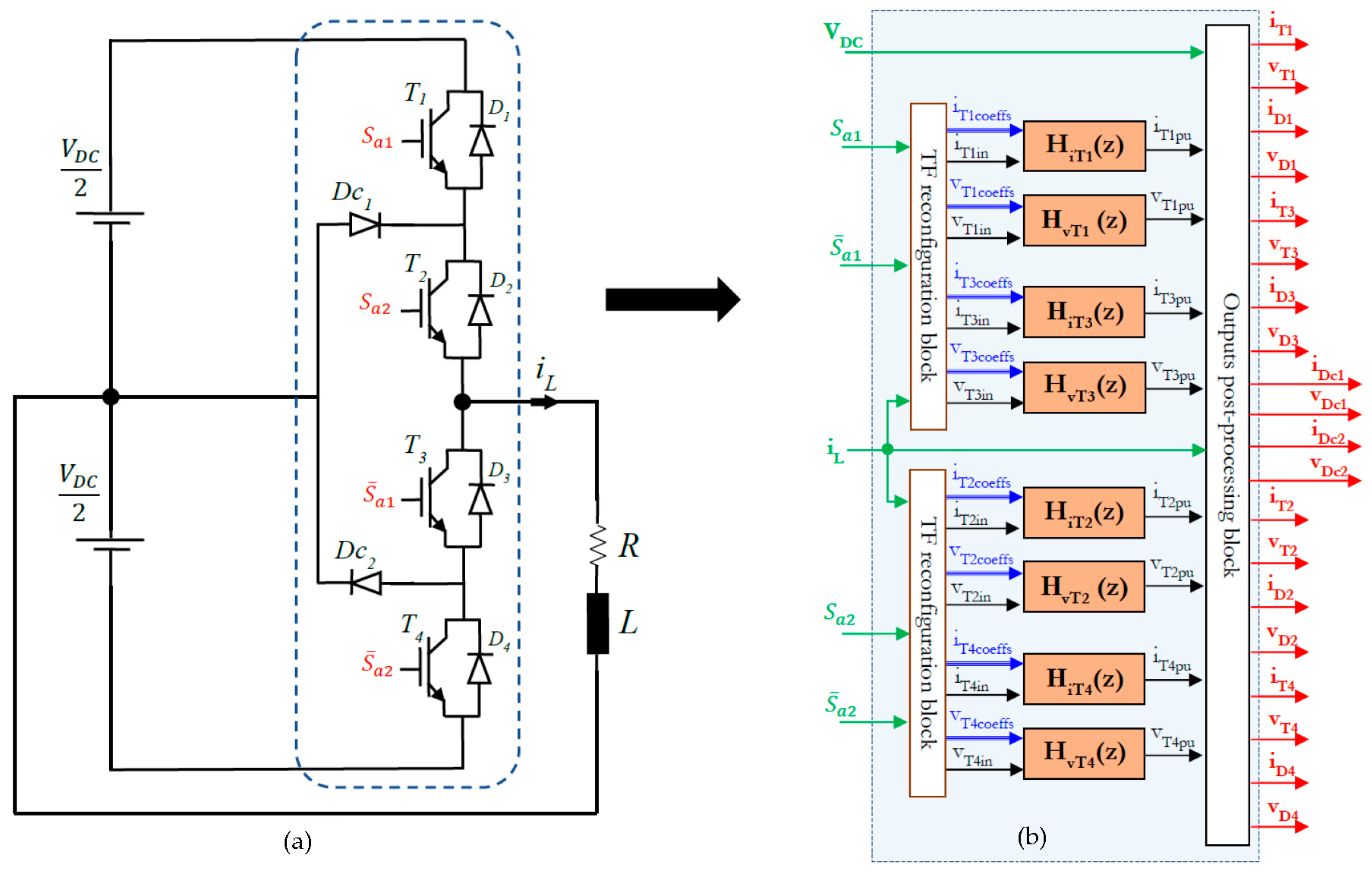
2. Main Basics of the Adopter Modeling Approach
This section aims to provide reminders about the adopted modeling approach, bearing in mind that an in-depth description was already proposed in [
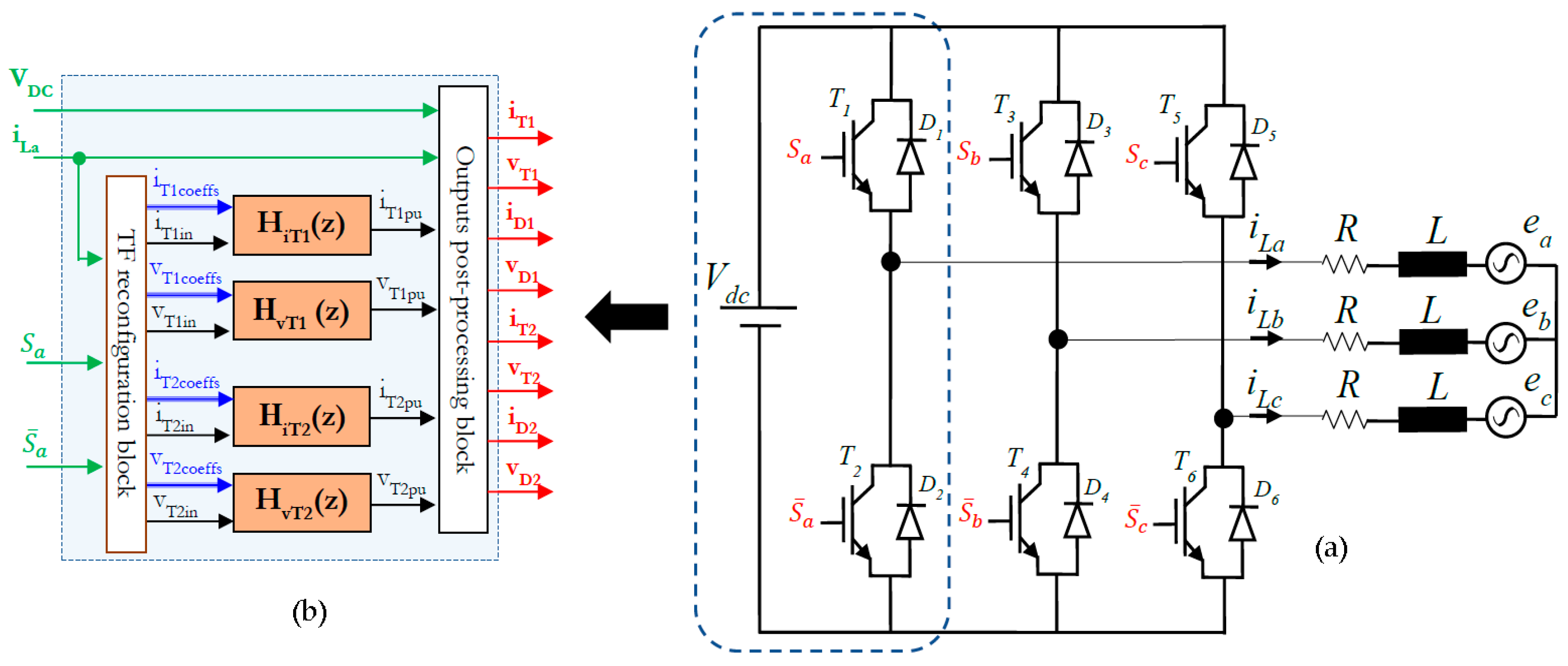
26]. To begin, let us consider a classical three-phase voltage source inverter that supplies an RLE load, as shown in
Figure 1a (this case study is detailed in
Section 3). The idea behind the proposed approach consists of extracting from the overall topology individual switching and complementary cells composed of two transistors and two diodes. Then, the equivalent RT models of these cells are interconnected according to the overall topology.
The main variables of concern are the currents/voltages of the transistors. The dynamics of each one are represented by coefficient-varying transfer functions (TFs). These coefficients vary, on the one hand, in order to gather both turn-ON and turn-OFF dynamics in a unique TF and, on the other hand, in order to approximate the actual behavior of each power switch. Then, the experimental voltage/current data of each transistor are periodically collected and provided to a system identification algorithm that generates the best fitting TF (in this work, the Matlab System Identification toolbox is used).
As can be seen in
Figure 1b, for each of the extracted commutation cells, four unified transfer functions (H
iT1(z), H
vT1(z), H
iT2(z), and H
vT2(z)) are then developed and executed simultaneously, providing a full parallel structure. The varying coefficients are previously stored in memories. At each simulation time step and depending on the switch state, they are adequately read and transferred to the appropriate TF block. Regarding the input of the TF block, it consists of a unit step that toggles depending on the switch state (i.e., depending on the steady-state value of the variable).
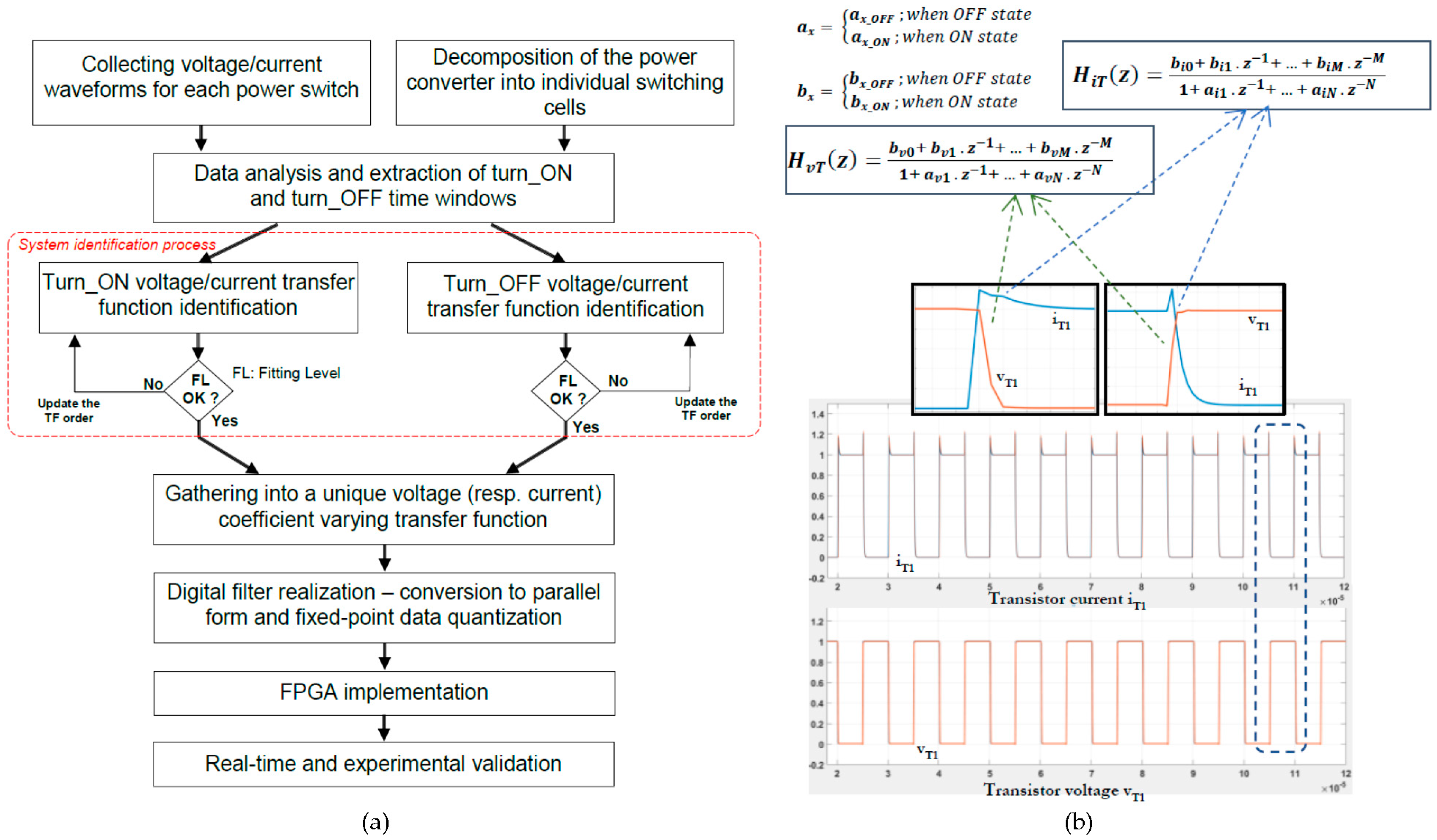
Figure 2a provides more details about the overall modeling process. The first step consists of isolating individual commutation cells and collecting the voltage/current waveforms. The turn-ON and turn-OFF time windows are then extracted before the system identification procedure. As illustrated in
Figure 2b, unified coefficient-varying TFs are generated for each time window and for each variable before being implemented and real-time tested.
2.1. System Identification Process
The values of the coefficients and the N-order of each TF depend on the desired fitting level during the system identification process. To this aim, Matlab/Simulink System Identification toolbox is deployed to generate discrete-time linear models from the measured voltage/current. The choice of the TF order depends on the desired approximation accuracy and fitting level (trial-and-error process with a threshold set to 90% in this work).
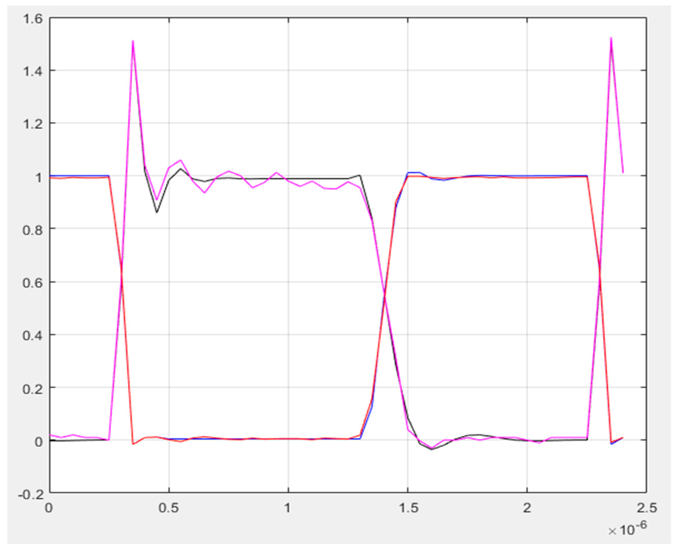
Figure 3 shows the approximation results obtained for a MOSFET SiC power switch (CMF20120D) that operates with a 500 kHz switching frequency. The measured per-unit voltage and current are sampled and averaged at a 50 ns time resolution (equal to the adopted simulation time step). For both commutations, the identification process is given 3rd-order transfer functions, with fitting levels satisfying the 90% constraint. They are expressed as figured out in the following equation and
Table 1.
2.2. TF Reconfiguration Block and Output Post-Processing
Let us go back to
Figure 1. The reconfiguration block allows the TF coefficients and inputs reconfiguration depending on the states of the commutation cell switches. The starting point is the examination of the gate signals S
a and the sign of the load current
iLa in order to determine the state of each transistor. When the state turns ON or OFF, the appropriate coefficients (that are stored in memories) are read and sent to each TF. Also, the unit-step input of the latter is accordingly toggled.
As for the output post-processing, the per-unit voltages and currents provided by the TFs are respectively rescaled with the measured VDC voltage and the load current iLa. Furthermore, the signs of these outputs are used to calculate the remaining diode variables. Note that in the case of HIL testing, the DC voltage and the load current can be processed respectively by dedicated source and load RT simulators.
2.3. Digital Realization and FPGA Implementation
Regarding the digital realization of the transfer functions, to make an efficient balance between the N-order of the transfer function and the execution time needed to process the outputs, a parallel digital form is adopted [
27]. This consists of transforming the initial structure into a parallel combination of 1st and 2nd digital filters. Thus, whatever the initial order, this combination always yields the same execution time and corresponds to a 2nd-order block.
Figure 4 shows the parallel form corresponding to the obtained 3rd-order structure of Equation (1).
As for the FPGA implementation, the whole designs that are presented in the following sections have been developed manually in VHDL and through the Xilinx ISE design platform, following a dedicated design methodology [
28]. All the RT validations are performed using the Artix-7 AC701 Evaluation Kit provided by Xilinx-AMD [
29]. The kit integrates an Artix-7 XC7A200T-2 device synchronized with a 200-MHz system clock. Regarding the hardware resources, this FPGA target includes 13 Mbits RAM blocks, 269,200 flip-flops, 134,600 lookup tables, and 740 DSP48E blocks, among others.
A deep analysis of the time/area performances corresponding to an individual commutation cell was conducted and provided in [
26]. Regarding the timing, the adopted simulation time step is fixed to 50 ns, and the total execution time has been evaluated to 45 ns (with a 200 Mhz system clock).
In the following sections, the eRTS of an individual commutation cell is extended and evaluated with more complex topologies, namely, a 3-phase VSI and a single-phase neutral-point clamped (NPC) VSI. Note that other topologies were evaluated in the previously published work, namely, a half-bridge DC–DC converter, a single-phase full-bridge DC–AC converter, and a single-phase multi-level cascaded H-bridge (5-level and 9-level).
3. Application to a Three-Phase Voltage Source Inverter
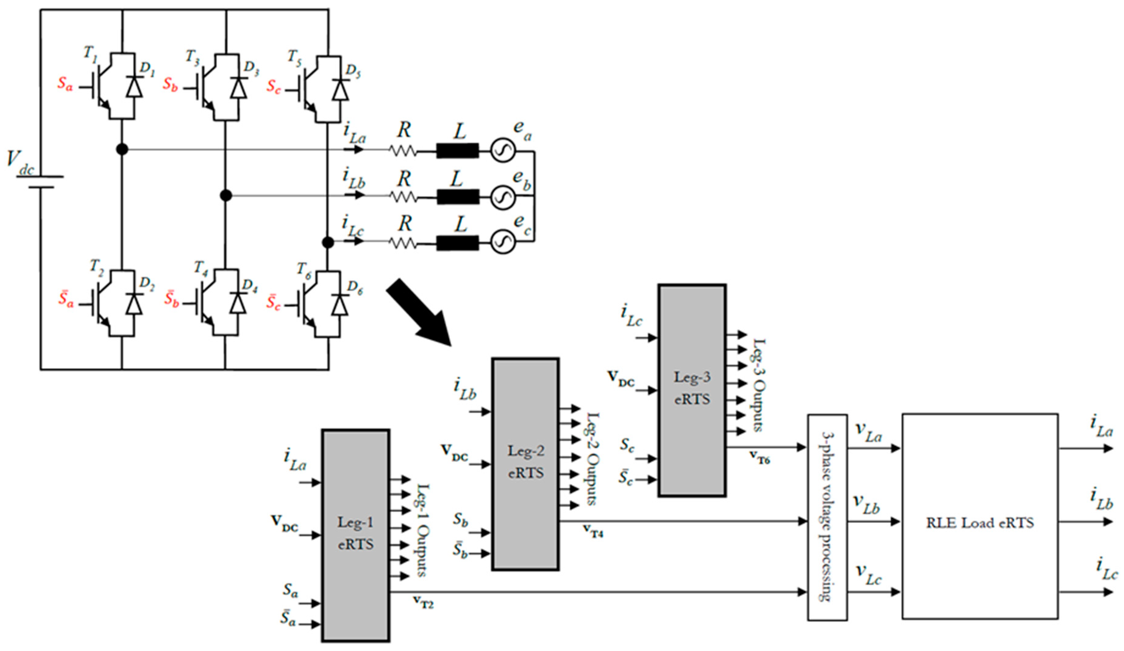
This section presents the eRTS of a three-phase VSI supplying a three-phase RLE load.
Figure 5 highlights the corresponding architecture. Each leg corresponding to a commutation cell is represented by a dedicated eRTS module (
Figure 5). Each one generates the voltages/currents of its inherent transistors/diodes. The voltages v
T2, v
T4, and v
T6 are used to generate the three-phase load voltages according to the following equation.
The supplied load consists of a three-phase balanced RLE series (R = 5 Ω; L = 15 mH). Its corresponding eRTS is based on the forward Euler discrete-time model that generates the load current according to the following equation:
where
;
;
; and
is the RT simulation time step (set to 50 ns).
The controller is not deepened in this paper but consists of generating three-phase sinusoidal voltage references assuming that the back-EMF terms are compensated. The amplitudes of these references are equally set to 0.25 pu (over VDC = 600 V) and their frequencies to 200 Hz. The switching signals are generated through a 100 kHz PWM module.
The overall architecture is implemented in the Xilinx Artix-7 XC7A200T-2 FPGA device, and a 200 MHz system clock is used for synchronization. The eRTS modules of the VSI legs and the load are both executed fully in parallel. With such organization, the total execution time is still equal to 45 ns, which allows operation with a 50 ns simulation time step. In terms of hardware resources and with the adopted fixed-point format (25Q18 for the leg eRTS and 32Q28 for the load), the overall design uses 6088 flip-flops, 3790 lookup tables (2.5% of the available slices), and 201 hardwired 25 × 18-bit DSP48E blocks (27% of the available blocks).
When it comes to the RT validation, the suggested figures highlight the waveforms of the main variables, collected with a 1 µs time resolution and using a Xilinx ChipScope platform [
29].
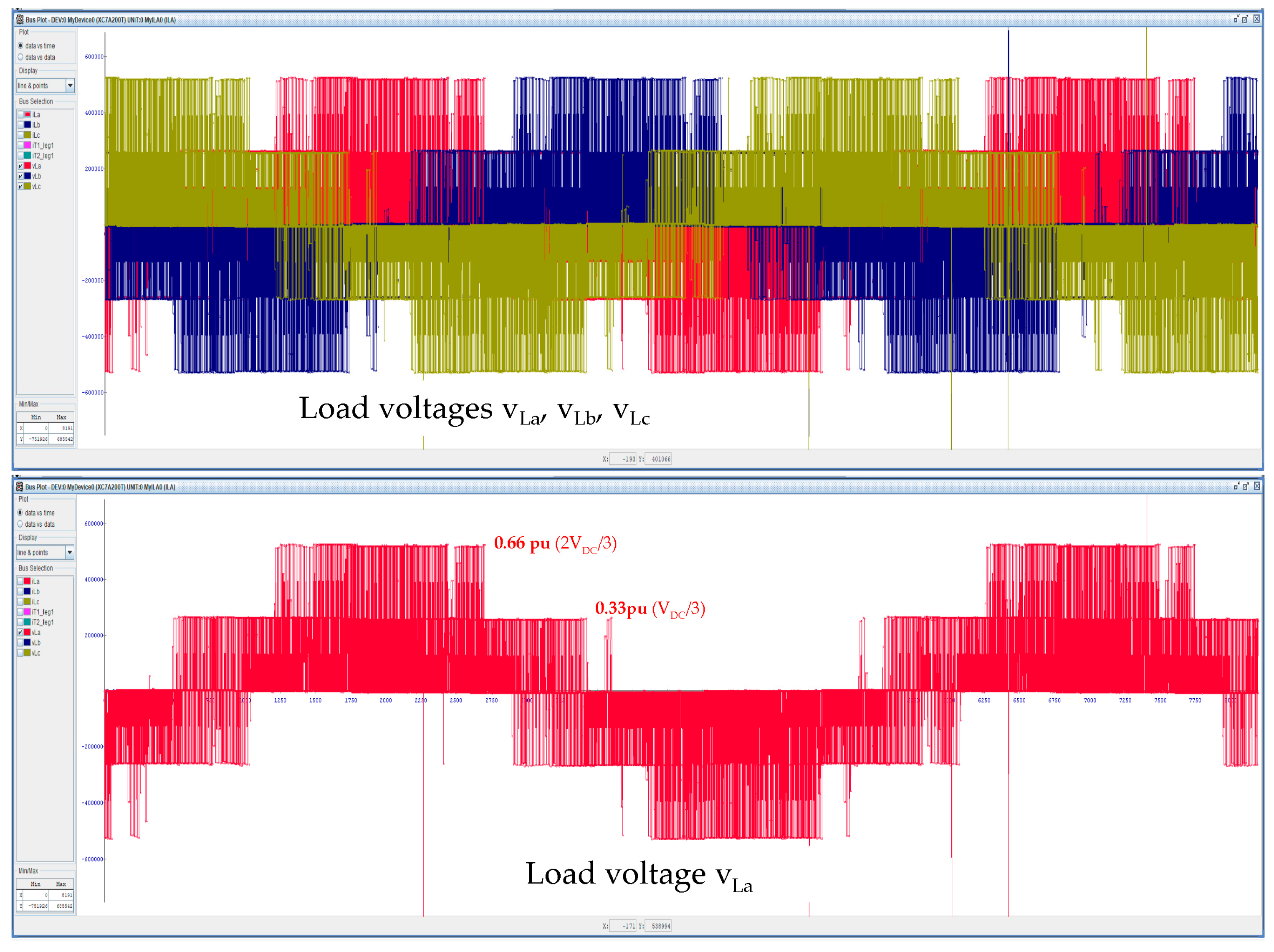
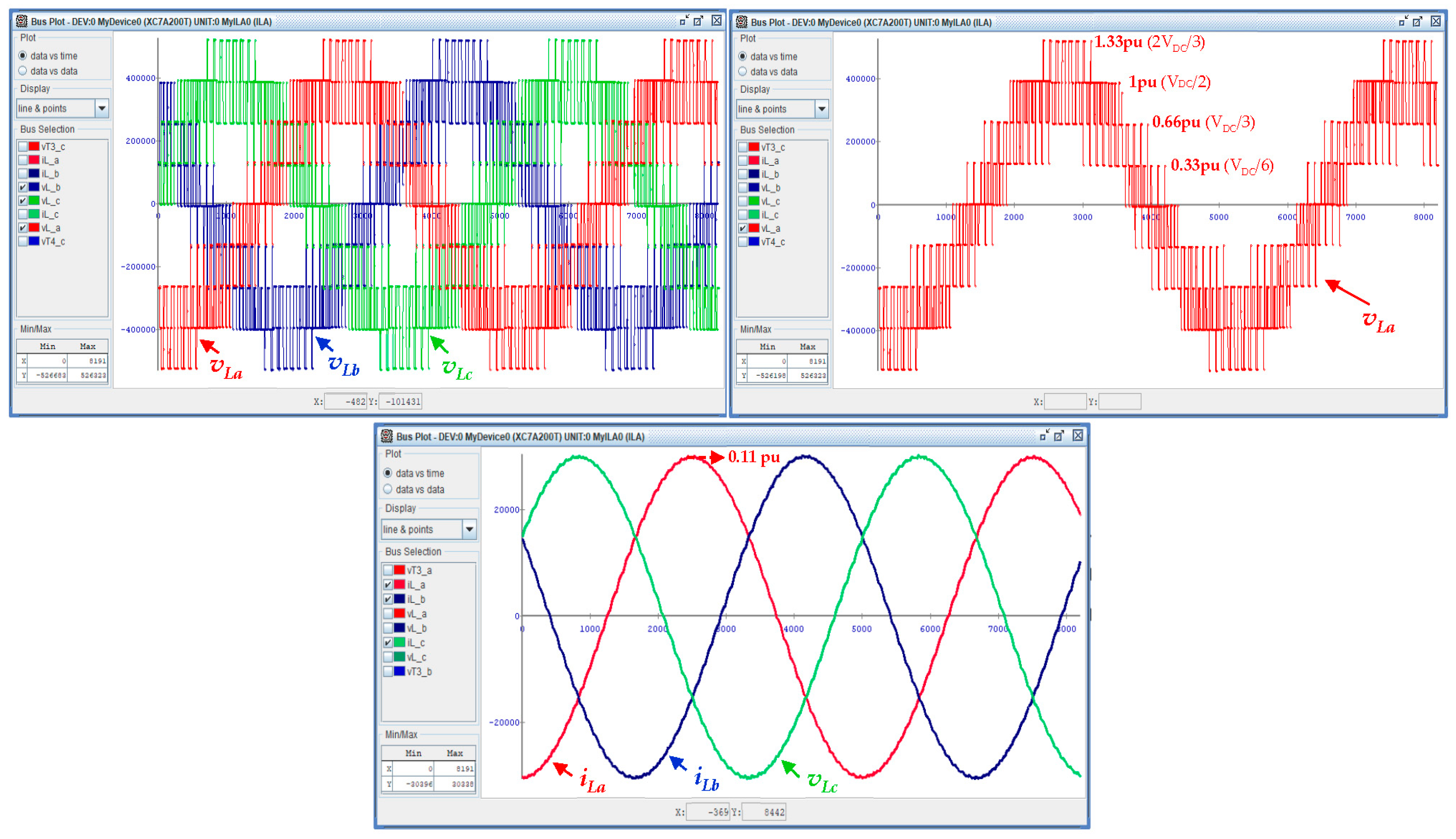
Figure 6 presents the waveforms of the per-unit three-phase voltages
vLa,
vLb, and
vLc. The evolution of transistor voltage and current at the commutation scale can be seen back with a better resolution in
Figure 3.
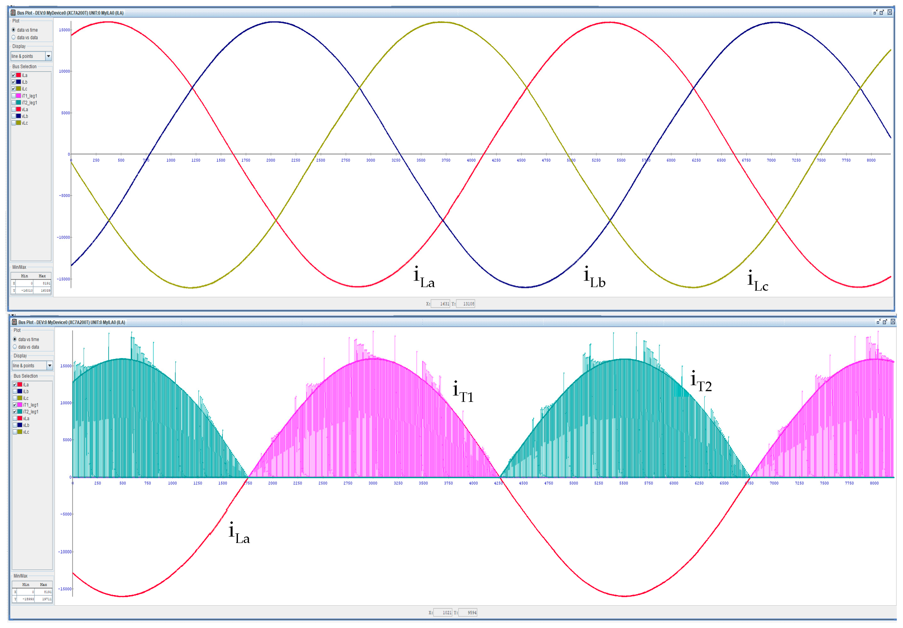
Regarding the currents,
Figure 7 highlights the per-unit waveforms of the three-phase load currents and those of T
1 and T
2 transistor currents. Here again, the evolution at the commutation scale can be seen with a better resolution in
Figure 3. In addition to their visual coherency, all the obtained FPGA results are the same as their Matlab/Simulink counterparts. The average fitting error, because of the limited fixed-point data format, is evaluated to be less than 1.5% with regard to the equivalent floating-point Matlab/Simulink simulation.
4. Application to a Neutral-Point Clamped Inverter
The proposed modeling approach is tested with a half-bridge NPC inverter supplying the RL load (R = 5 Ω; L = 15 mH). As can be seen in
Figure 8a, its topology integrates a combination of two commutation cells in a single leg, respectively driven by (
and (
. This is why the equivalent eRTS introduces eight transfer functions organized as H
iT1(z), H
vT1(z), H
iT3(z), and H
vT3(z) for the first commutation cell and H
iT2(z), H
vT2(z), H
iT4(z), and H
vT4(z) for the second one, as shown in
Figure 8b. Each group is associated with its appropriate reconfiguration block, and all the per-unit outputs are gathered in the post-processing block, which generates all the rescaled variables of the inverter.
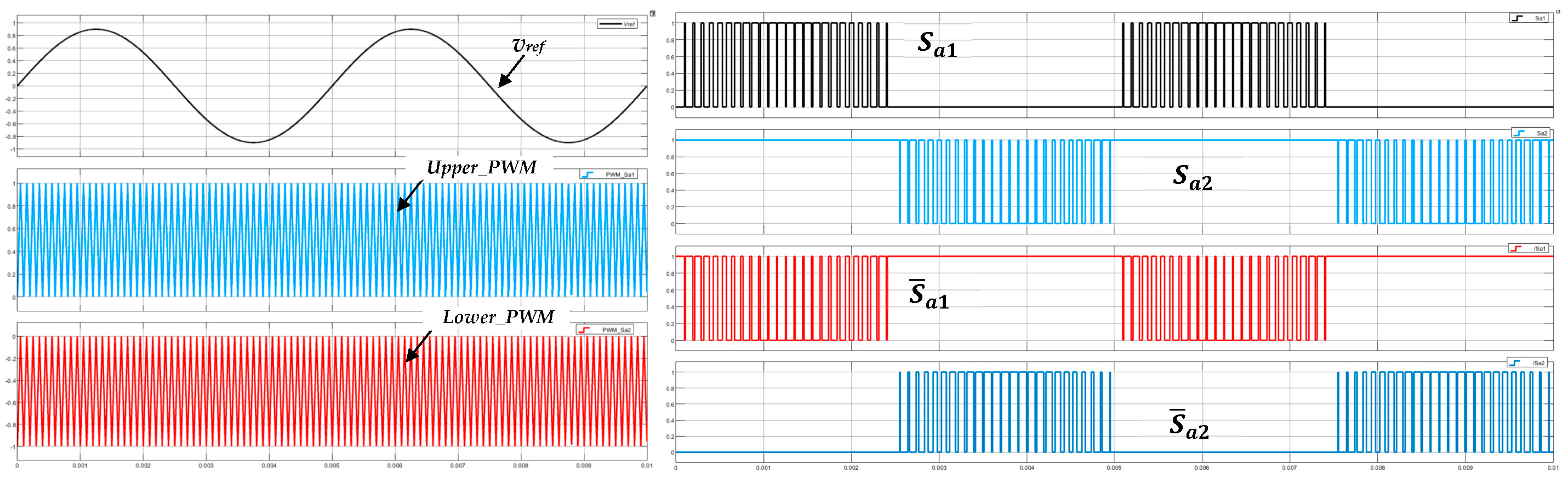
An open-loop controller id implemented for this case study. A sinusoidal voltage reference od applied with 0.9 pu amplitude (over V
DC/2 = 300 V) and 200 Hz frequency. The switching signals (
and (
are generated based on two 10 kHz PWM carriers, and the corresponding waveforms are highlighted in
Figure 9. In addition, (
are generated by comparing the voltage reference to the upper PWM carrier and (
by comparing to the lower one.
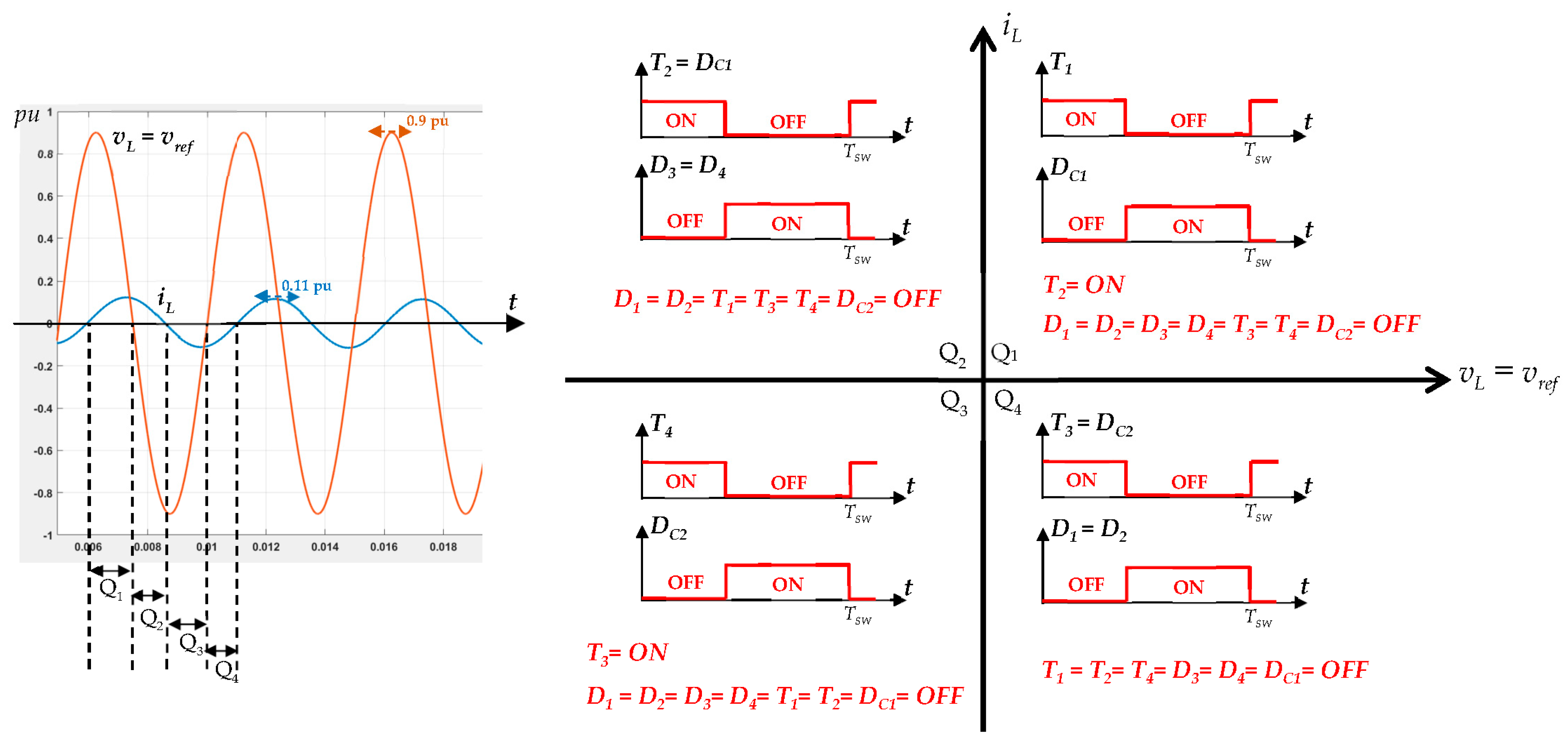
Based on this switching behavior, one can summarize the NPC operation using the four-quadrant characteristics of the load voltage (considering the sinusoidal reference) and the load current, as shown in
Figure 10. For each quadrant, the states of the power switches are given.
Like the previous case study, the overall design is developed and RT-tested with the Xilinx Artix-7 XC7A200T-2 FPGA device. The parallel structure of the designed NPC eRTS allows the preservation of the same timing performances as before, namely, a 45 ns execution time with the 200 MHz clock (thus, a 50 ns simulation time step). In terms of hardware resources and with the adopted fixed-point format (25Q18 for the leg eRTS and 32Q28 for the RL load), the overall design uses 4320 flip-flops, 2617 lookup tables (1.6% of the available slices), and 124 hardwired 25 × 18-bit DSP48E blocks (16.7% of the available blocks).
Figure 11 and
Figure 12 provide the obtained RT results. They are collected with a 1 µs time resolution and using a Xilinx ChipScope platform [
29]. As a general comment, knowing that the same transfer functions are used for all the tested topologies, the approximation quality remains at the same level of satisfaction, with a very low average error compared to the Matlab/Simulink results. In
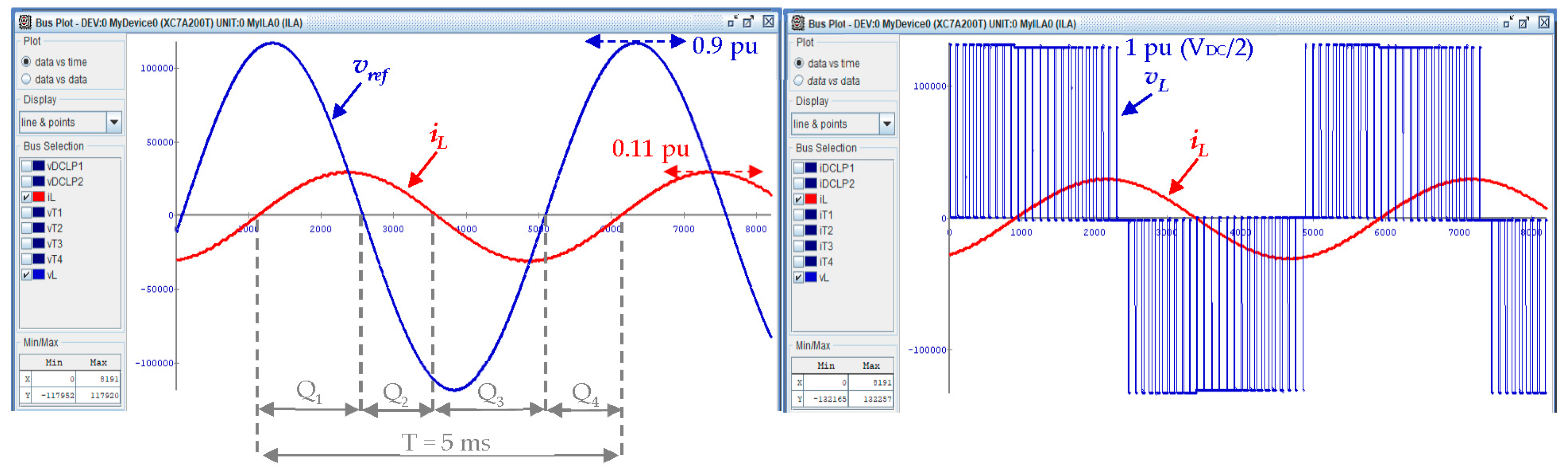
Figure 11, the waveform of the load current is shown in the same graph as the reference voltage (on the left side) and the inverter output voltage (on the right side). The above-described four quadrants are also highlighted, which may help in analyzing the remaining waveforms provided in
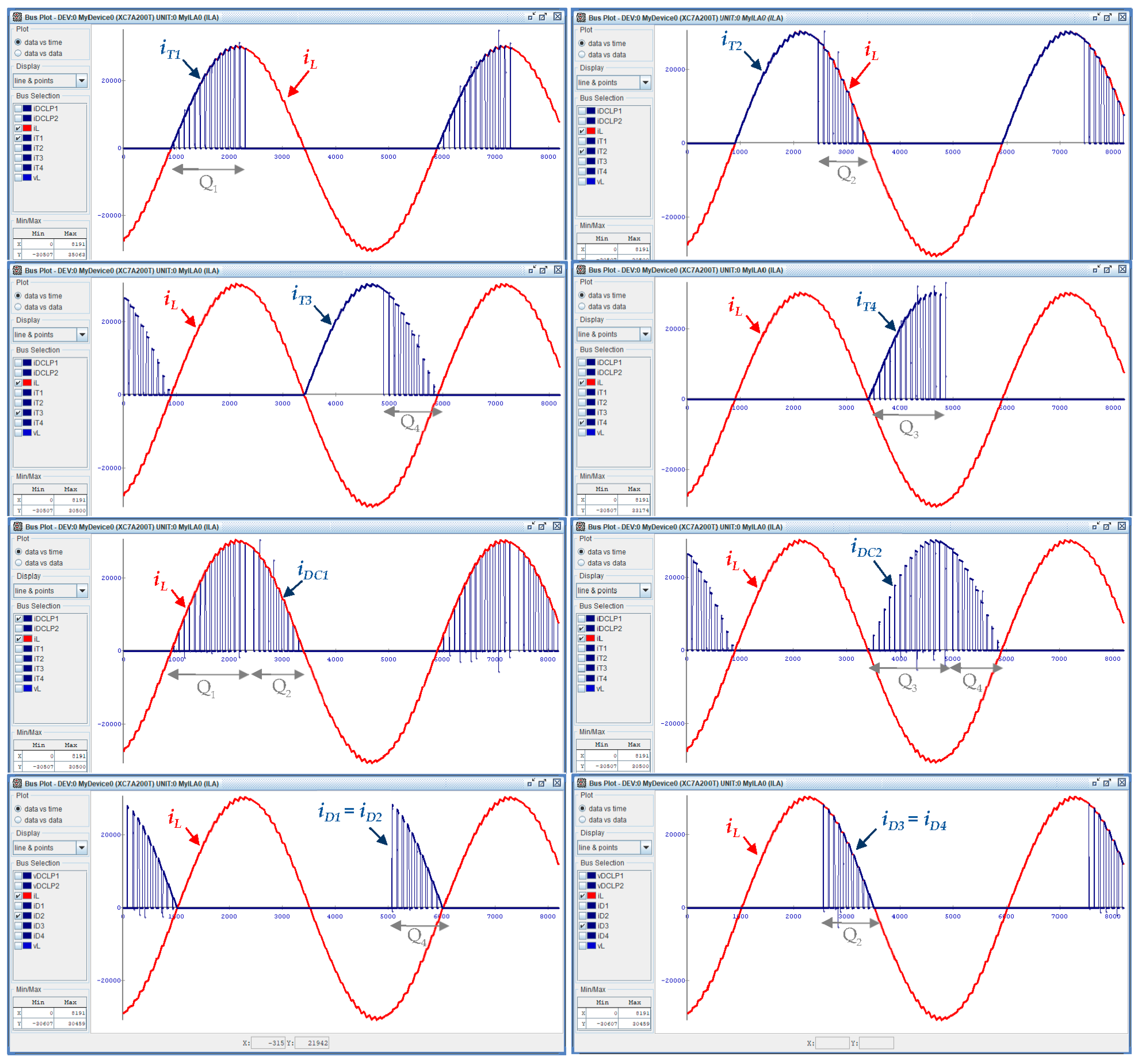
Figure 12. Indeed, the figure shows the evolution of the current in each power switch and successfully confirms the switching configurations given for each quadrant.
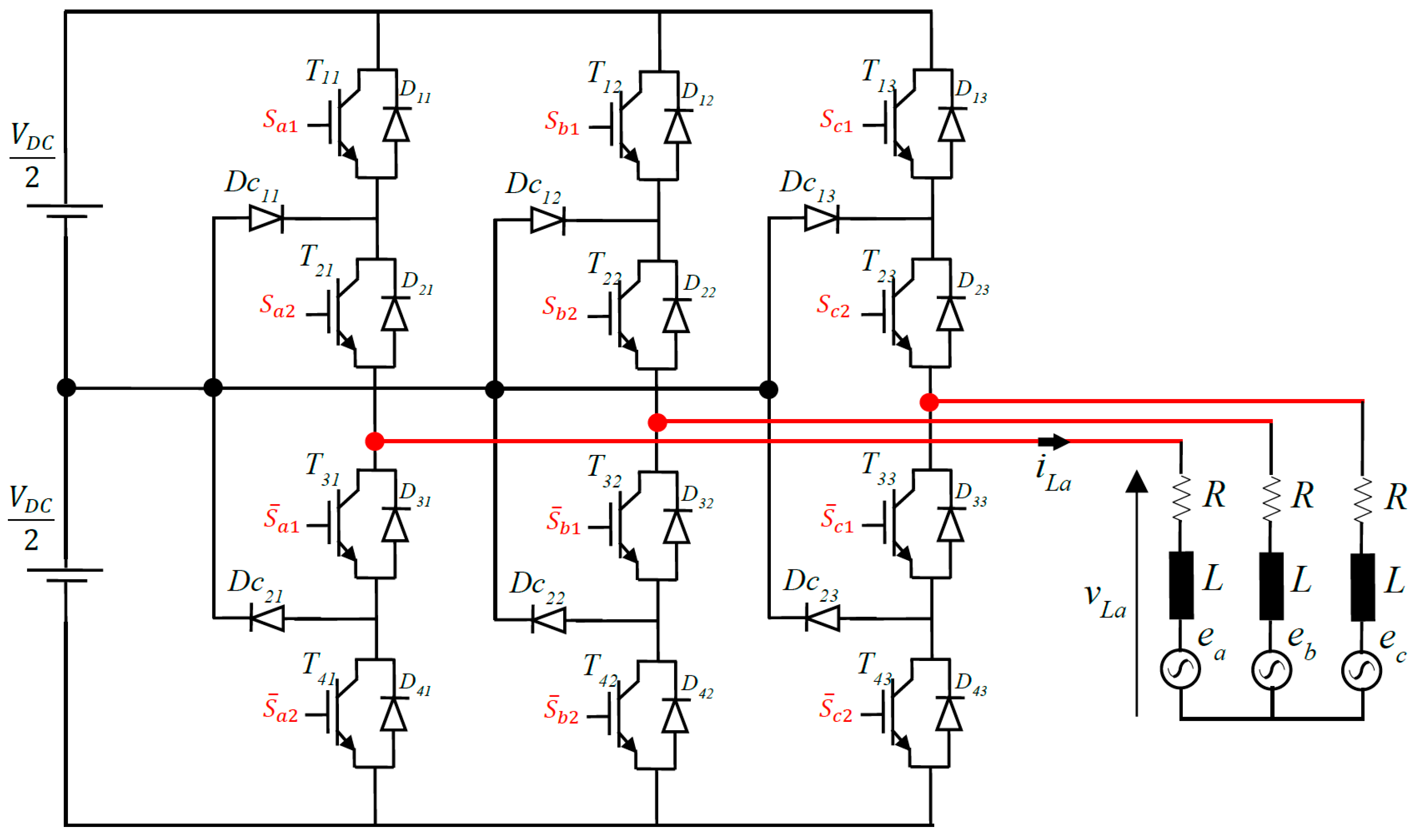
These evaluations are extended to a three-phase NPC structure that supplies an RLE load.
Figure 13 shows the tested circuit. Like the three-phase VSI case (
Figure 5), each leg is represented by its dedicated eRTS, allowing a full parallelization of the design and then maintaining the same timing performances as before (45 ns execution time, 50 ns simulation time step). Regarding the hardware resources and with the adopted fixed-point format (25Q18 for the leg eRTS and 32Q28 for the load), the overall design uses 10,703 flip-flops, 6055 lookup tables (3.9% of the available slices), and 372 hardwired 25 × 18-bit DSP48E blocks (50% of the available blocks).
The controller generates three-phase sinusoidal voltage references assuming that the back-EMF terms are compensated. The amplitudes of these references are equally set to 0.9 pu (over V
DC/2 = 300 V) and their frequency to 200 Hz. The 10 kHz PWM process can be seen in
Figure 9. The RT results obtained with this operating condition are highlighted in
Figure 14, which shows the load voltages (
vLa,
vLb,
vLc) and the load currents (
iLa,
iLb,
iLc). They are compared with Matlab/Simulink equivalent simulations, and the limited fixed-point precision (25Q18 format) introduces an average fitting error of less than 2%.
5. Conclusions
This paper presents the design of a full parallel FPGA-based adaptive eRTS of power electronic converters. The proposed approach introduces the possibility of approximating the static and dynamic behavior of power switches based on real measurements and through a system identification process. By doing so, the end-user electrical/thermal operating conditions of the power converter can be considered in the RT model. The commutation transients are then approximated using transfer functions with varying coefficients. The values of the coefficients vary depending on the turn-ON or turn-OFF states, and they can be periodically updated to consider the scalable operating conditions. Then, all the collected coefficient data are stored in memory blocks and read adequately at each simulation time step. Regarding the FPGA implementation, a full parallel design is developed at each hierarchical level of the power converter. The corresponding FPGA architectures are rigorously synchronized, allowing us to optimize the total latency, achieve low execution time (Tex = 45 ns with 200 MHz clock), and consequently guarantee a low RT simulation time step (Tsim = 50 ns).
However, several challenges have to be managed with the proposed approach. At first, to achieve a high level of fidelity of the real system, the acquisition chain, including sensors and analog to digital converters, must have a high level of dynamical performance. This critical challenge must be associated with a high-precision system identification algorithm. Furthermore, in the perspective of developing real-time digital twins, this identification algorithm must be designed for an online execution, which induces, in contrast, additional implementation issues. Regarding these issues, we demonstrate that the parallel structuration of the eRTS allows a very short execution time regardless of the order of the transfer functions. However, it is fair to notice that additional efforts have to be conducted to optimize the FPGA resources, especially when dealing with complex converter topologies.
This paper can be considered a prolongation of a previous work where the modeling approach was described in detail. The proof of concept was tested with different topologies, including half-bridge DC–DC, full-bridge DC–AC, and multi-level (five-level and nine-level) cascaded H-bridge DC–AC converters. In this paper, the main basics are recalled, and more importantly, additional case studies are presented, namely, namely a three-phase VSI, a half-bridge NPC inverter, and a three-phase NPC inverter. The obtained results have comforted additional investigations and this is specifically the case of system identification, where online identification algorithms are under study.


