Article

Low-Power Current Integrating Flat-Passband Infinite Impulse Response Filter for Sensor Read-Out Integrated Circuit in 65-nm CMOS Technology

Department of Nano & Semiconductor Engineering, Tech University of Korea, Siheung 15073, Republic of Korea
Electronics 2023, 12(5), 1191; https://doi.org/10.3390/electronics12051191
Submission received: 12 January 2023 / Revised: 22 February 2023 / Accepted: 23 February 2023 / Published: 1 March 2023
(This article belongs to the Special Issue CMOS Chips for Sensing and Communication)

Abstract

:
Low-power current integrating infinite impulse response filter having flat-passband for sensor read-out integrated circuit is proposed. In a current integrating filter, passband flatness degradation is inevitable due to sinc-like filtering characteristics. In this paper, by proposing a high order infinite impulse response filter architecture, flat-passband characteristic can be achieved. By implementing a filter architecture with a flat passband, the required sampling frequency can be lowered, which in turn can reduce power consumption. Moreover, the proposed high order infinite impulse response filter architecture has a high degree of freedom on adjusting input sample weights. The proposed integrated circuit is implemented in TSMC 65-nm CMOS process and operated on 1.2 V supply voltage.

1. Introduction

The analog filter adopted in existing integrated circuits has limited reconfigurability. That is, to change the filtering characteristics, sizes of passive components such as resistors or capacitors must be varied or the transconductance must be adjusted over a wide range [1,2,3]. On the other hand, current integrating filters have high reconfigurability, making them suitable for integrated circuits because their filtering characteristics can be changed by adjusting the ratio of sampling capacitances or clock frequencies [4,5,6,7]. However, current integrating filters cannot avoid flatness degradation in the passband because of their inherent sinc shaped frequency response, which causes signal-to-noise ratio (SNR) degradation and worsens the adjacent channel selectivity (ACS) [8,9].
There have been many attempts to reduce passband flatness degradation. Current integrating band-pass analog infinite impulse response (IIR) filters having inverse sinc-like frequency response have been proposed [10]. Through a cascade connection with a band-pass analog IIR filter, the sinc shaped frequency response can be compensated for. However, due to limitation of implementable filter coefficients of band-pass analog IIR filters, these filters cannot be applied for all shapes of frequency response. As a compensation method, digital inverse finite impulse response (FIR) filters using digital signal processing (DSP) on the digital back-end are suggested [11]. However, this approach requires additional power consumption and chip area.
Likewise, to achieve the flat-passband frequency response, high sampling frequency for low-pass analog IIR filter is adopted [12,13,14]. Even though an analog baseband filter is used, sampling frequency is in the range of several hundred MHz. If signal bandwidth is increased, sampling frequency would then increase several times. In other words, increased sampling frequency causes increased power consumption of clock generator and imposes a burden on the analog-to-digital converter (ADC). In this paper, as a solution to the flatness degradation of the current integrating analog filter, a low-pass analog IIR filter having a flat passband is proposed; this filter does not require any compensation or high sampling clock frequency.

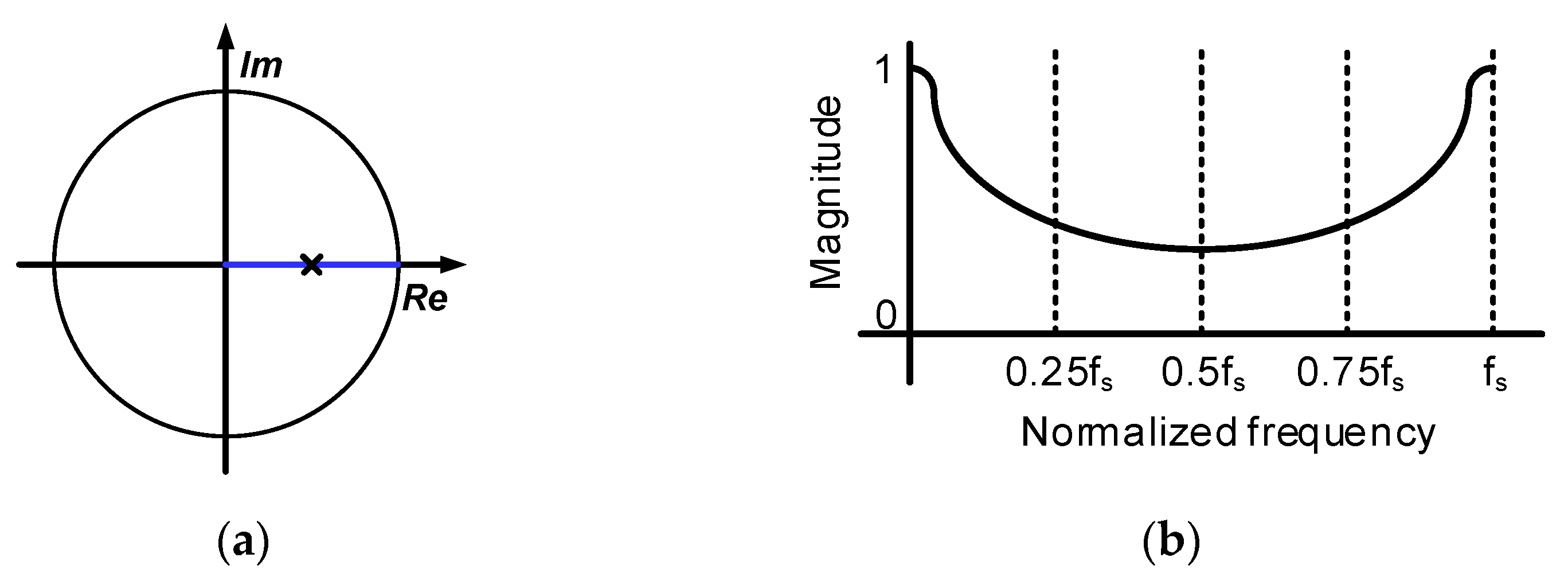
2. Current Integrating Analog IIR Filter Topology

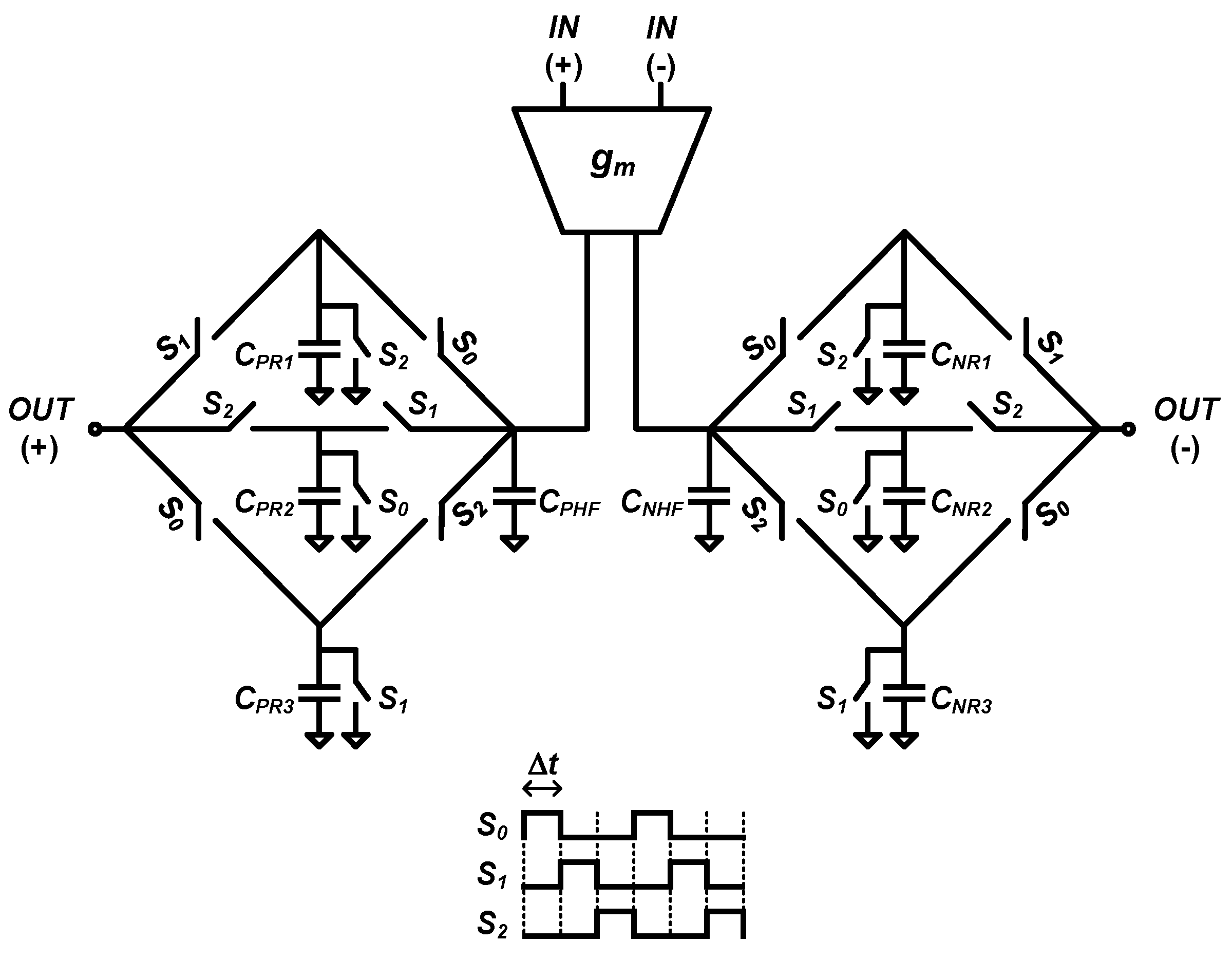
2.1. Conventional Architecture

The conventional architecture for a current integrating analog IIR filter is shown in Figure 1 [5,6,7]. An operation diagram is presented in Table 1. Input signal is converted from voltage to current by the transconductance amplifier. When switch S0 is ON, the input signal is integrated into capacitor CPR1 and CPHF at a ratio α:(1 − α). After that, the charges stored in CPR1 are read out and then discharged. However, the charges stored in CPH1 are not discharged. Therefore, CPHF contains information of previous input signals, and the corresponding charges are transferred to CPR1 to form a filter having IIR characteristics. Its transfer function in the z-domain is expressed as
H ( z ) = 1 α 1 α z 1     where     α = C H F C H F + C R A s s u m e     C H F = C P H F = C N H F     a n d     C R = { C P R 1 , P R 2 , a n d   P R 3 } = { C N R 1 , N R 2 , a n d   N R 3 }
Pole-zero plot and magnitude response are shown in Figure 2. Conventional current integrating analog IIR filter has only one pole [7], hence flat passband cannot be implemented. Since the pole is always located on the right-half real axis according to the capacitance ratio α, frequency response has a maximum magnitude at f = 0, and gradually decreases up to f = 0.5 fs.

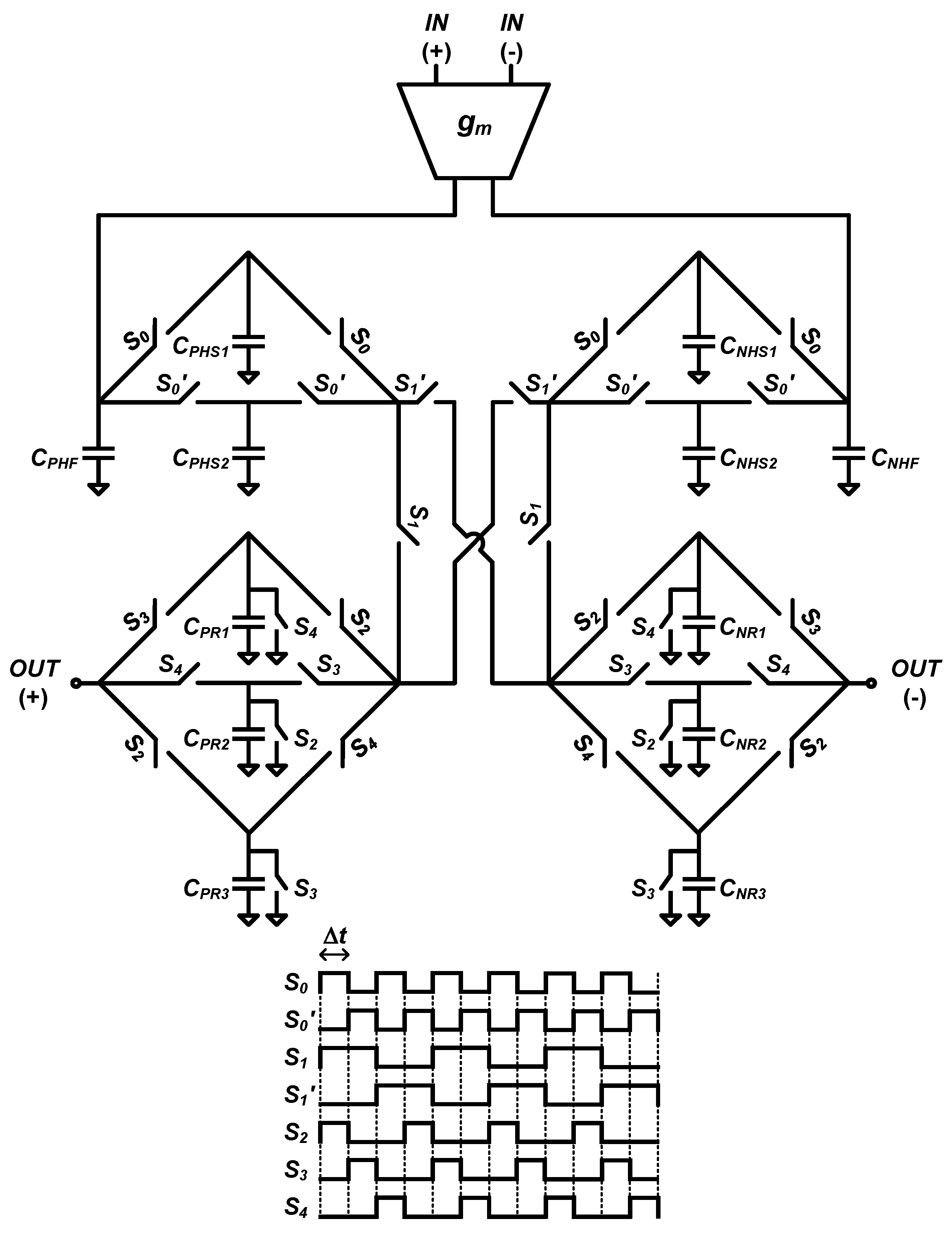
2.2. Proposed Architecture

The current integrating flat-passband analog high order IIR filter having two poles is proposed as shown in Figure 3. The operation diagram is presented in Table 2. Current input signal is utilized by adopting a transconductance amplifier. During the on-state of switches S0, S1, and S2, input signal on positive path is stored in CPHF, CPHS1, and CPR1 at a ratio of α:β:γ. At the same time, input signal on negative path is stored in CNHF, CNHS1, and CNR1 at a ratio of α:β:γ. During the on-state of switch S3, the charges in CPR1 are read out. Afterward, CPR1 is discharged during the on-state of switch S4. On the other hand, input charges stored in CPHF are not discharged. That is, previous input charges accumulate in non-discharged capacitor CPHF, and then affect the next sampling operation. Hence, the once-delayed operation, z−1, is implemented using the non-discharged capacitor CPHF. Likewise, input charges stored in CPHS1 and CPHS2 are not discharged. Based on the differential architecture, both CPHS1 and CPHS1 operate at 50% duty cycle, that is, they operate in the on-state of switches S0 or S0′. In addition, they are alternately connected to positive and negative paths. Hence, accumulated input charges affect sampling operation once per two periods. Eventually, the plus-signed twice-delayed operation, z−2, can be implemented. Transfer function of the proposed filter in the z-domain is given by
H ( z ) = γ 1 α z 1 + β z 2 where   α = C H F C H F + C H S + C R ,   β = C H S C H F + C H S + C R ,     a n d   γ = C R C H F + C H S + C R A s s u m e     C H F = C P H F = C N H F   ,     C H S = { C P H S 1     a n d     P H S 2 } = { C N H S 1     a n d     N H S 2 }   ,     a n d     C R = { C P R 1 , P R 2 , a n d   P R 3 } = { C N R 1 , N R 2 , a n d   N R 3 }
As shown in Figure 4, instead of one pole locating on the right-half real axis in the conventional architecture, two poles are located on the right-half complex plane if α and β have a relation of α < 2 β . The pole locations are expressed as
p o l e { 1   a n d   2 } = ( α 2   , ± | α 2 4 β | 2 )
Through adjustment of the pole locations, magnitude of frequency response can be equalized within a certain range. For implementation of flat passband, not a 3 dB cut-off frequency, but a 0.3 dB cut-off frequency is adopted where the magnitude difference compared to f = 0 is about 0.3 dB. This can be expressed as
| | H ( ω ) | f = 0   | H ( ω ) | f = cut - off | 0.3   d B

2.3. Transconductance Amplifier

The proposed architecture is operated on the basis of current integration. For this purpose, a fully differential transconductance amplifier (TA) [11] is employed; its schematic is shown in Figure 5. It contains a source-coupled differential-pair input stage that can provide high common-mode rejection. Furthermore, variation of DC operating point on output node has an effect on signal swing and causes linearity degradation. Thus, to minimize change of the output DC operating point, the common-mode feedback (CMFB) is adopted. Moreover, current mirrors having a size ratio of M boost their output currents M times. Transconductance can be expressed as
g m = M μ n C o x ( W L ) ( V g s V t h )

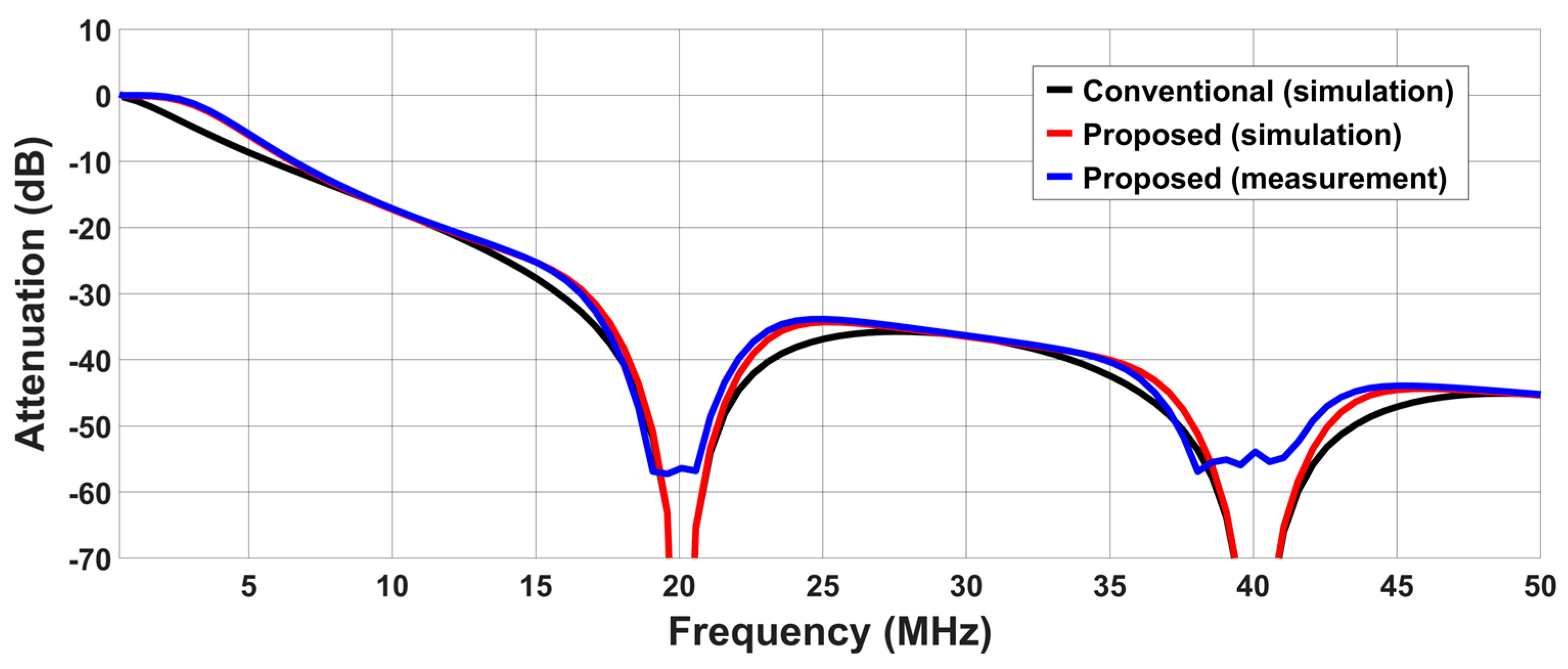
3. Measurement Results

Frequency response of proposed architecture is shown in Figure 6. Black and red lines indicate simulated frequency responses of conventional and proposed architecture, respectively. Blue line indicates measured frequency response of proposed architecture. Sampling frequency was set to 20 MHz. To obtain the correct frequency response, the S21 scattering parameter was measured using a network analyzer. Passband degradation of approximately 1.8 dB at passband edge was obtained. Compared to existing analog filter, the current integrating filter did not have ripples in the passband. The proposed architecture had nulls at the integer multiples of the sampling frequency because of windowed integration [7]. The null depth had a finite value and, as the frequency increased, the null depth decreased. An important factor determining the null depth in the frequency response of the current integrating filter was the output impedance of the transconductance amplifier [5]. The output resistance of the transconductance amplifier was reduced by the influence of the parasitic resistance, which resulted in a decrease in null depth. A two-tone test was carried out to measure the linearity of the proposed architecture. Two-tone signals at 9.5 MHz and 17.5 MHz were adopted, and IM3 power at 1.5 MHz was measured. Figure 7 shows IIP3 measured with sampling frequency of 20 MHz. The IIP3 was measured and found to be −6 dBm. Furthermore, the noise figure was measured and found to be approximately 40 dB at 1 MHz. Chip micrograph is shown in Figure 8. Proposed architecture was implemented using a TSMC 65-nm CMOS process and operated on 1.2 V supply voltage.

4. Discussion

4.1. Performance Comparison

In this paper, in order to verify a high order infinite impulse response filter having flat-passband characteristics, a second order infinite impulse response filter was implemented. In particular, filter coefficients of α = 0.6 and β = 0.2 are required to obtain flat-passband characteristics in the second order infinite impulse response filter. However, as shown in Equation (6), in the previous architecture, since filter coefficients α and β are defined as multiplication and addition among sampling capacitors, there are restrictions on determining coefficients α and β [12]. Thus, in the previous architecture, filter coefficients α = 0.6 and β = 0.2 cannot be realized with any combination of sampling capacitors.
H ( z ) = γ 1 α z 1 + β z 2 where   α = C H F C H F + C R + C H S C H S + C R ,   β = C H F C H F + C R C H S C H S + C R ,    a n d   γ = C R C H F + C R C H S C H S + C R
On the other hand, as shown in Equation (2), in the proposed architecture, since the filter coefficients α and β are determined as the ratio among the sampling capacitors, it has a high degree of freedom in determining the filter coefficients. Therefore, filter coefficients α = 0.6 and β = 0.2 for flat-passband characteristics can be implemented. However, it has a restriction that the sum of α and β cannot exceed 1.
In systems where current integrating filters are used, high sampling frequencies have been adopted [12,13,14]. In other words, when the sampling frequency increases, the signal bandwidth stretches, and thus the 3 dB cut-off frequency increases. Thus, the flatness degradation of the passband seemed to be mitigated somewhat by using a very high sampling frequency relative to the signal bandwidth. By adopting proposed flat-passband architecture, a sampling frequency can be reduced to several tens of MHz while maintaining signal bandwidth, which can lead to lower power consumption.
In addition, in the previous architecture, the order of the filter must be increased to increase the stop band attenuation, which has the disadvantage of reducing the signal bandwidth. However, if the cascade connection of proposed architecture is implemented or a higher order filter is implemented, the stop band attenuation can be increased while maintaining the signal bandwidth.
Furthermore, bandwidth-to-sampling frequency ratio (BSR) is defined as
B S R = B a n d w i d t h   [ M H z ] S a m p l i n g   f r e q u e n c y   [ M H z ]
Bandwidth refers to the range of frequencies in a system within which the signal’s magnitude is at least −3 dB of its maximum value. Design of power efficient manner can be distinguished by using the index of BSR. Proposed architecture shows the BSR of 0.19, which means high power efficiency compared to previous architectures. In the current integrating filter, most of the power is consumed in gm-cell and clock generator. A clock generator with a high sampling frequency accounts for the largest portion of the system’s power consumption. In particular, the power consumption of the clock generator is determined in proportion to the sampling frequency. In the proposed architecture, a current integrating filter with flat-passband characteristics is implemented while using a low sampling frequency, which enabled low-power operation. The performance comparisons are summarized in Table 3. Proposed architecture has a 3 dB bandwidth of about 3.8 MHz, and a sampling frequency of 20 MHz was used. Previous works have used sampling frequencies of hundreds of MHz to implement 3 dB bandwidths of several MHz. In addition, because the proposed architecture performs a non-decimation operation, it is free from aliasing issues. The proposed integrated circuit is fabricated in TSMC 65-nm CMOS technology and operates with 1.2 V supply voltage. The current consumption of gm-cell and clock generator is 0.25 mA and 0.04 mA, respectively. In particular, since the proposed architecture implements a 3 dB bandwidth of several MHz while using a low sampling frequency, it shows low power consumption compared to previous works.

4.2. Related Application

Nowadays, sensor systems composed of multiple sensors of different types are widely used [15,16]. The sensor system consists of a sensor and a read-out circuit, and the read-out circuit consists of an amplifier and a filter as shown in Figure 9. In order to process multiple sensors in a readout circuit, a time-division multiplexing method using switching network is mainly adopted [17,18]. That is, one read-out circuit is utilized in common, and the type of sensor connected to the input terminal is changed through switching networks. Thus, in order to amplify and filter the output signals of multiple sensors of different types by using one common read-out circuit, a reconfigurable circuit architecture is required. The proposed filter having high reconfigurability can be usefully adopted for sensor systems. In addition, low power operation is possible by lowering the required sampling frequency through flat-passband implementation. Therefore, it is suitable for the multi-sensor system that is widely used in the internet of things (IoT) era.

5. Conclusions

A low-power current integrating flat-passband analog infinite impulse response filter architecture is proposed. Even using a low sampling frequency, flat-passband characteristics can be obtained through the proposed architecture, and thus power consumption can be reduced. The current integrating filter is suitable for multi-sensor systems; using this filter, sensor read-out integrated circuits having high reconfigurability could be implemented. The proposed integrated circuit was implemented in a TSMC 65-nm CMOS process.

Funding

This work was supported by the National Research Foundation of Korea (NRF) grant funded by the Korea government (MSIT) (No. 2020R1F1A1076859).

Data Availability Statement

Not applicable.

Acknowledgments

The EDA Tool was supported by the IC Design Education Center, Korea.

Conflicts of Interest

The author declares no conflict of interest.

References

  1. Wang, X.; Boon, C.C.; Yang, K.; Kong, L. A 20–80 MHz Continuously Tunable Gm-C Low-Pass Filter for Ultra-Low Power WBAN Receiver Front-End. IEEE Access 2021, 9, 154136–154142. [Google Scholar] [CrossRef]
  2. Wang, Y.; Wu, B.; Huang, H. A 3rd/5th Order Active RC Chebyshev Analog Baseband Low-Pass Filter with Reconfigurable Bandwidth and Gain. IEEE Access 2021, 9, 129319–129328. [Google Scholar] [CrossRef]
  3. Lavalle-Aviles, F.; Sanchez-Sinencio, E. A 0.6-V Power-Efficient Active-RC Analog Low-Pass Filter with Cutoff Frequency Selection. IEEE Trans. Very Large Scale Integr. (VLSI) Syst. 2020, 28, 1757–1769. [Google Scholar] [CrossRef]
  4. Zheng, J.; Ki, W.-H.; Tsui, C.-Y. A Fully Integrated Analog Front End for Biopotential Signal Sensing. IEEE Trans. Circuits Syst. I Regul. Pap. 2018, 65, 3800–3809. [Google Scholar] [CrossRef]
  5. Jiang, W.; Zhu, Y.; Chan, C.-H.; Murmann, B.; Martins, R.P. A 7-Bit 2 GS/s Time-Interleaved SAR ADC with Timing Skew Calibration Based on Current Integrating Sampler. IEEE Trans. Circuits Syst. I Regul. Pap. 2021, 68, 557–568. [Google Scholar] [CrossRef]
  6. Liu, C.-C.; Huang, M.-C. 28.1 A 0.46mW 5MHz-BW 79.7dB-SNDR Noise-Shaping SAR ADC with Dynamic-Amplifier-Based FIR-IIR Filter. In Proceedings of the 2017 IEEE International Solid-State Circuits Conference (ISSCC), San Francisco, CA, USA, 5–9 February 2017. [Google Scholar]
  7. Zhou, Y.; Filiol, N.M.; Yuan, F. A Quadrature Charge-Domain Sampling Mixer with Embedded FIR, IIR, and N-Path Filters. IEEE Trans. Circuits Syst. I Regul. Pap. 2015, 62, 1431–1440. [Google Scholar] [CrossRef]
  8. Ge, X.; Theuwissen, A.J.P. A 0.5erms−Temporal Noise CMOS Image Sensor with Gm-Cell-Based Pixel and Period-Controlled Variable Conversion Gain. IEEE Trans. Electron Devices 2017, 64, 5019–5026. [Google Scholar] [CrossRef] [Green Version]
  9. dos Santos, F.V.; Dogaru, E. Flexible Wideband Radio Transceiver Testing Using Non-Uniform Subsampling Demodulation. In Proceedings of the 2018 IEEE International Symposium on Circuits and Systems (ISCAS), Florence, Italy, 27–30 May 2018. [Google Scholar]
  10. Yoshizawa, A.; Iida, S. Parasitic Discrete-Time-Pole Cancelling Techniques for Ultra-Wideband Discrete-Time Charge-Domain Baseband Filters. In Proceedings of the 2010 IEEE Asian Solid-State Circuits Conference, Beijing, China, 8–10 November 2010. [Google Scholar]
  11. Huang, M.-F.; Kuo, M.-C.; Yang, T.-Y.; Huang, X.-L. A 58.9-DB ACR, 85.5-DB SBA, 5–26-MHz Configurable-Bandwidth, Charge-Domain Filter in 65-nm CMOS. IEEE J. Solid-State Circuits 2013, 48, 2827–2838. [Google Scholar] [CrossRef]
  12. Tohidian, M.; Madadi, I.; Staszewski, R.B. A 2 mW 800 MS/s 7th-Order Discrete-Time IIR Filter with 400 kHz-to-30 MHz BW and 100 dB Stop-Band Rejection in 65 nm CMOS. In Proceedings of the 2013 IEEE International Solid-State Circuits Conference Digest of Technical Papers, San Francisco, CA, USA, 17–21 February 2013. [Google Scholar]
  13. Bozorg, A.; Staszewski, R.B. A Charge-Sharing IIR Filter with Linear Interpolation and High Stopband Rejection. IEEE J. Solid-State Circuits 2022, 57, 2090–2101. [Google Scholar] [CrossRef]
  14. Payandehnia, P.; Maghami, H.; Mirzaie, H.; Kareppagoudr, M.; Dey, S.; Tohidian, M.; Temes, G.C. A 0.49–13.3 MHz Tunable Fourth-Order LPF with Complex Poles Achieving 28.7 DBm OIP3. IEEE Trans. Circuits Syst. I Regul. Pap. 2018, 65, 2353–2364. [Google Scholar] [CrossRef]
  15. Chan, W.P.; Narducci, M.; Gao, Y.; Cheng, M.-Y.; Cheong, J.H.; George, A.K.; Cheam, D.D.; Leong, S.C.; Damalerio, M.R.B.; Lim, R.; et al. A Monolithically Integrated Pressure/Oxygen/Temperature Sensing SoC for Multimodality Intracranial Neuromonitoring. IEEE J. Solid-State Circuits 2014, 49, 2449–2461. [Google Scholar] [CrossRef]
  16. Fick, L.; Fick, D.; Alioto, M.; Blaauw, D.; Sylvester, D. A 346 um 2 VCO-Based, Reference-Free, Self-Timed Sensor Interface for Cubic-Millimeter Sensor Nodes in 28 nm CMOS. IEEE J. Solid-State Circuits 2014, 49, 2462–2473. [Google Scholar] [CrossRef]
  17. Tang, Z.; Fang, Y.; Yu, X.-P.; Shi, Z.; Tan, N. A CMOS Temperature Sensor with Versatile Readout Scheme and High Accuracy for Multi-Sensor Systems. IEEE Trans. Circuits Syst. I Regul. Pap. 2018, 65, 3821–3829. [Google Scholar] [CrossRef]
  18. Liu, L.; Gao, D.; Tian, Y.; Yu, Y.; Qin, Z. A Low Mismatch and High Input Impedance Multi-Channel Time-Division Multiplexing Analog Front End for Bio-Sensors. IEEE Sens. J. 2022, 22, 6755–6763. [Google Scholar] [CrossRef]
Figure 1. Conventional architecture of current integrating infinite impulse response filter.
Electronics 12 01191 g001
Figure 2. Conventional architecture (a) pole-zero plot and (b) magnitude response.
Electronics 12 01191 g002
Figure 3. Proposed architecture of current integrating flat−passband infinite impulse response filter.
Electronics 12 01191 g003
Figure 4. Proposed architecture (a) pole−zero plot and (b) magnitude response.
Electronics 12 01191 g004
Figure 5. Schematic of transconductance amplifier.
Electronics 12 01191 g005
Figure 6. Measured frequency response of proposed architecture.
Electronics 12 01191 g006
Figure 7. Measurement results of two−tone test.
Electronics 12 01191 g007
Figure 8. Chip micrograph.
Electronics 12 01191 g008
Figure 9. Multi-sensor read-out integrated circuit as an example application of proposed current integrating flat-passband infinite impulse response filter.
Electronics 12 01191 g009
Table 1. Operation diagram of conventional architecture. CS, RO, D and S stand for charge sampling, read−out, discharging, and sharing, respectively.
Operation DiagramClock State
S0S1S2
Sampling capacitor
on positive path
CPHFSSS
CPR1CSROD
CPR2DCSRO
CPR3RODCS
Sampling capacitor
on negative path
CNHFSSS
CNR1CSROD
CNR2DCSRO
CNR3RODCS
Table 2. Operation diagram of proposed architecture. CS, RO, D and S stand for charge sampling, read-out, discharging, and sharing, respectively.
Operation DiagramClock State
S0S0S1S1S2S3S4
Sampling capacitor
on positive path
CPHFSS-----
CPHS1S------
CPHS2-S-----
CPR1----CSROD
CPR2----DCSRO
CPR3----RODCS
Sampling capacitor
on negative path
CNHFSS-----
CNHS1S------
CNHS2-S-----
CNR1----CSROD
CNR2----DCSRO
CNR3----RODCS
Table 3. Performance comparison between the proposed and the previous architectures.
Proposed Architecture[12][13][14]
DecimationNoneNoneNoneNone
3 dB
bandwidth [MHz]
3.80.4 to 301 to 9.90.49 to 13.3
Sampling
frequency [MHz]
20800333300
BSR0.190.0005 to 0.03750.003 to 0.0330.0016 to 0.044
Supply
voltage [V]
1.21.20.91.8
Current consumption of gm-cell [mA]0.250.230.361.05
Current consumption of clock generator [mA]0.041.40.661.33
Power [mW]0.351.960.924.3
Technology65-nm
CMOS
65-nm
CMOS
28-nm
CMOS
180-nm
CMOS
Disclaimer/Publisher’s Note: The statements, opinions and data contained in all publications are solely those of the individual author(s) and contributor(s) and not of MDPI and/or the editor(s). MDPI and/or the editor(s) disclaim responsibility for any injury to people or property resulting from any ideas, methods, instructions or products referred to in the content.

