Abstract
In this study, we designed an MOS varactor for application in the differential voltage-controlled oscillator (VCO). To improve the quality factor of the MOS varactor, we proposed a symmetric layout technique of the MOS varactor with reduced parasitic components. Compared with the typical MOS varactor layout, the metal line for the interconnection of the MOS varactors that is inevitable in the typical MOS varactors for the cross-coupled VCO was minimized to reduce the parasitic resistance. In addition, with the reduced interconnection metal line, the overall size of the proposed MOS varactor was also reduced compared with the typical one. To verify the feasibility of the proposed MOS varactor structure, the typical and proposed MOS varactors were designed using a 180 nm RFCMOS process. Compared to the typical MOS varactor, the measured quality factor of the proposed MOS varactor was improved by approximately 32% at the operating frequency of 5.0 GHz. Additionally, we successfully verified that the parasitic capacitance induced by the lossy silicon substrate was reduced in the proposed MOS varactor structure.
1. Introduction
With an advancement in electronic devices, the need for wireless communication technology continues to increase. The voltage-controlled oscillator (VCO) is one of the key components in wireless communication systems. In general, the cross-coupled VCO is popular for GHz-order RF systems because of its low-phase noise characteristics [1]. Accordingly, studies on various modified VCOs based on the cross-coupled type have been actively conducted [2,3,4,5,6,7,8,9]. However, as RF systems become more sophisticated to cover a higher data rate, further improvements in the phase noise of the VCO are required.
Such phase noise is one of the most important indicators of the VCO’s performance, and many studies related to the phase noise have been conducted. Based on Lesson’s model, the phase noise of L(Δω) of the VCO with the LC tank can be derived as follows:
where PS, ω0, QL, and Δω0 are the average power dissipated in the parasitic resistance of the LC tank, the oscillation frequency, the effective quality factor of the LC tank, and the offset from the carrier frequency, respectively. Δω1/f3 is the frequency of the corner between the 1/f3 and 1/f2 regions. This implies that the quality factor of the LC tank affects the phase noise of the VCO [10]. Therefore, in order to improve the phase noise, it is important to improve the quality factor by minimizing the parasitic resistance of the inductor, capacitor, and MOS varactor constituting the LC tank [11,12,13].
Many extant studies have attempted to minimize the parasitic resistance induced by the spiral inductor of the LC tank to improve the phase noise of the VCO. Although the parasitic resistance induced by the spiral inductor degrades the phase noise of the VCO the most significantly, the low quality factor of the MOS varactor that is essential in the VCO also degrades the phase noise of the VCO significantly [14,15]. Moreover, given the channel resistance and complicated structure of the MOS varactor, the varactor itself has a relatively low quality factor compared to the metal–insulator–metal (MIM) capacitor. Additionally, if the size of the MOS varactor is increased to improve the frequency tuning range of the VCO, the quality factor of the MOS varactor is further deteriorated.
In this work, we propose a layout technique that can improve the quality factor by reducing the parasitic resistance component of the MOS varactor for VCO applications. In Section 2, the quality factor of the MOS varactor is investigated, and the proposed layout technique of the MOS varactor is described in Section 3. Measurement results to verify the effectiveness of the proposed layout technique are shown in Section 4.
2. Quality Factor of the LC Tank with MOS Varactor
Figure 1 shows the typical cross-coupled VCO with a differential structure. As shown in Figure 1a, two MOS varactors are essential to obtain the symmetrical differential signal and to block the dc voltage of the control voltage, VCTRL. Therefore, the metal line to connect two MOS varactors is also required between two MOS varactors. However, the interconnection metal line causes additional parasitic components, which can further degrade the quality factor of the LC tank. Figure 1b shows the parasitic components induced via the contact and metal line. In particular, the contact that is essential for the interconnection of the metal lines significantly degrades the quality factor of the MOS varactors. Consequently, to improve the phase noise of the VCO, the loss induced by the interconnection metal line should be suppressed.
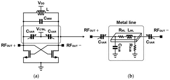
Figure 1.
Typical cross-coupled VCO with LC tank: (a) schematic and (b) equivalent circuit of the parasitic components of the interconnection metal line.
To investigate the effect of the MOS varactors on the quality factor of the LC tank, we analyzed the simple LC tank structure shown in Figure 2. As shown in Figure 2b, to obtain the required tuning range of the operation frequency of the VCO, the MOS varactor was used in parallel with the MIM capacitor. In general, the quality factor of the MIM capacitor is much higher than that of the MOS varactor. Accordingly, if the capacitance of the MOS varactor increases to expand the tuning range of the operation frequency, the overall quality factor of the LC tank may be deteriorated. In Figure 2c, the MOS varactors with an interconnection line are shown. For the convenience of analysis, the equivalent circuit of the interconnection metal line was simplified to parasitic resistance and inductance.
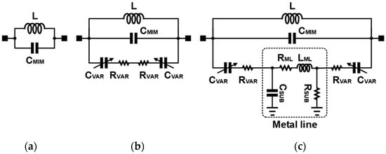
Figure 2.
Simple structure of LC tank: (a) typical LC tank, (b) LC tank with varactors, and (c) LC tank with varactors and interconnection metal line.
The quality factor of the LC tank can be expressed as follows [15,16]:
where QLC, QL, and QC are the quality factors of the LC tank, inductor, and capacitor, respectively. Considering the MOS varactor for frequency tuning, the QC can be expressed as follows:
where C, CMIM, CVAR, and QVAR are the total capacitance of the LC tank, the capacitances of the MIM capacitor and MOS varactor, and the quality factor of the MOS varactor including the interconnection metal line, respectively. In this case, considering the parasitic components of the interconnection metal line for two MOS varactors, QVAR can be expressed as follows:
where RVAR and RML are the parasitic resistances of the MOS varactor and interconnection metal line. As a result, QLC with parasitic components of the MOS varactors and interconnection metal line can be calculated as follows:
Here, CSUB and RSUB in Figure 2c were ignored in the equations for the convenience of analysis. As can be seen in the analyzed QLC, the metal line for the two MOS varactors degrades the overall quality factor of the LC tank, and consequently the performance of the VCO can be degraded.
The degradation of QLC via the interconnection metal line can also be confirmed by the simulation results in Figure 3. In Figure 3, electromagnetic simulation was performed by increasing the length of the interconnection metal line. The length of the metal line being zero means an ideal case without an interconnection metal line. As can be seen in Figure 3, QLC was degraded as the length of the interconnection metal line increased. In addition, since the parasitic capacitance occurs between the metal line and the silicon substrate, the parasitic capacitance of the metal line also increased as the length increased. The parasitic capacitance of the metal line also causes power loss and is one of the reasons for the deterioration of QLC. The parasitic capacitance shown in Figure 3b includes CSUB by the metal line and parasitic capacitance in the varactor. As a result of analysis and simulation, the degradation of the quality factor by the metal line cannot be ignored.
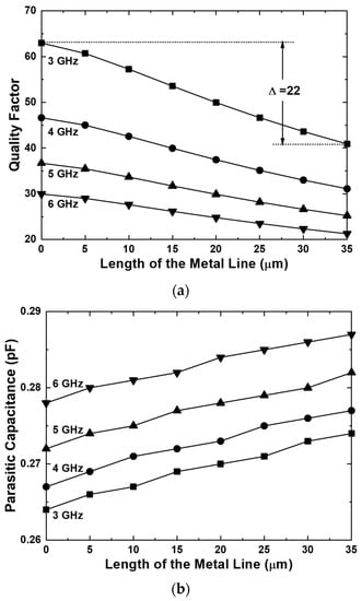
Figure 3.
Simulation results of the MOS varactors with zero VCTRL: (a) quality factor and (b) parasitic capacitance.
3. Proposed MOS Varactor Structure
In this study, we proposed a layout technique for two varactors that can remove the degradation of the quality factor caused by the metal line by removing the metal line located between the two varactors. Figure 4 shows the conceptual layouts of the typical and proposed MOS varactors.
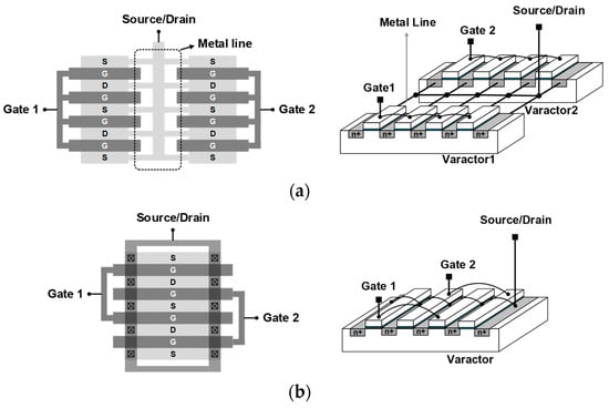
Figure 4.
Conceptual layouts of (a) typical and (b) proposed MOS varactors.
Generally, in the cross-coupled VCO, as shown in Figure 4, two MOS varactors face each other. The VCTRL for tuning the capacitance is applied through a node in which two MOS varactors are connected to each other. In general, each MOS varactor consists of unit-transistors in the form of a finger, combining the drain and the source to form a single node. As described above, it is essential to use a metal line for connecting two MOS varactors to each other in the typical structure of Figure 4a.
For cross-coupled VCO applications, two MOS varactors are required in the case of the typical structure. On the other hand, in the case of the proposed structure, a cross-coupled VCO can be applied with only one MOS varactor, as shown in Figure 4b. As shown in Figure 4b, the proposed structure was formed by grouping both drains and sources of the MOS varactor into one node. On the other hand, in the case of the gate nodes, gates that are not adjacent to each other were connected to each other, and as a result, two gate nodes were formed. In this work, as shown in Figure 4b, the two gate nodes are indicated as Gate 1 and Gate 2, respectively. The right side of Figure 4b is a conceptual diagram to aid understanding, and the actual layout is similar to the left side of Figure 4b. As a result, in the proposed structure, two MOS varactors were designed to share sources and drains with each other, and eventually the two MOS varactors were combined into one MOS varactor. Therefore, in the proposed MOS varactor structure, the interconnection metal line which is essential in the typical structure was removed, resulting in the removal of parasitic resistance and capacitance of the metal line. Accordingly, the quality factor of the proposed structure can be improved compared with the quality factor of the typical structure.
As described above, the two MOS varactors for the typical structure were combined into one MOS varactor for the proposed structure. Therefore, the MOS varactor of the proposed structure doubles the total gate width compared to the MOS varactor of the typical structure. The method of increasing the total gate width of the MOS varactor for the proposed structure aims to increase the unit gate width or the number of fingers. In the case of the method of increasing the number of fingers, the length of the MOS varactor may be excessively long, and thus the metal lines forming the Gate 1 and Gate 2 nodes are also lengthened, which may cause the quality factor to degrade again. Therefore, in this study, the unit gate width was increased to increase the total gate width of the MOS varactor for the proposed structure.
Figure 5 shows the simulation results of the quality factors of the MOS varactor according to the unit gate width. The results in Figure 5 are the simulation results of the MOS varactor itself, not the MOS varactor with a differential structure. In addition, if the gate length increases excessively, the parasitic resistance increases excessively, so the gate length was set to 4, 6, and 8 μm. As the total gate width of the MOS varactor increased, the dependence of the quality factor on the unit gate width weakened. In general, to expand the tuning range of the operation frequency, the total gate width of the MOS varactor should increase. In this study, the total gate width of the MOS varactor was selected for the 5.0 GHz applications. The total gate width of the MOS varactor was chosen to be 192 μm. Consequently, it can be seen that the unit gate width of the MOS varactor with the proposed structure increased; however, the degradation of the quality factor is insignificant, accordingly.
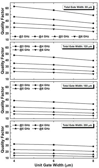
Figure 5.
Simulation results of the quality factors of the MOS varactor according to the total gate width with VCTRL of 0.0 V.
4. Measurement Results
To verify the feasibility of the proposed MOS varactor structure, we designed the MOS varactors with typical and proposed structures using a 180 nm RFCMOS process. The photographs of the designed MOS varactors are shown in Figure 6. In this study, the selected unit gate width was 4 μm. As shown in Figure 6, the interconnection metal lines for the MOS varactor were removed in the proposed structure. Accordingly, the parasitic components induced by the interconnection metal lines were also removed.
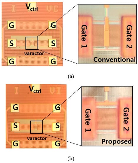
Figure 6.
Chip photographs of the designed MOS varactors: (a) typical and (b) proposed structures.
For a fair comparison, the total gate width of the two MOS varactors for the typical structure and the total gate width of the MOS varactor for the proposed structure were designed to be the same. The core sizes of the typical and proposed MOS varactors were 42 × 33 μm2 and 32 × 33 μm2, respectively. As a result, the size of the proposed structure decreased by approximately 23.8% compared to the size of the typical structure.
In the measurement, the VCTRL varied from 0.0 V to 2.4 V. Figure 7 shows the measured quality factors and capacitances according to operation frequency. As can be seen in Figure 7, because of the parasitic capacitance of the interconnection metal line of the typical structure, the capacitance of the typical structure was higher than that of the proposed structure. With VCTRL of 2.4 V, the measured capacitances of the typical and proposed structures were approximately 0.32 pF and 0.25 pF, respectively. On the other hand, in the case of the variable range of the capacitance according to the VCTRL, the proposed structure was measured to be wider than the typical structure. In addition, the proposed structure was measured to have a higher quality factor regardless of the VCTRL compared to the typical structure. The measurement results in Figure 7 showed the same tendency as the simulation results in Figure 3. That is, as the interconnection metal line of the typical structure was removed from the proposed structure, the parasitic capacitance of the proposed structure decreased and the quality factor increased.
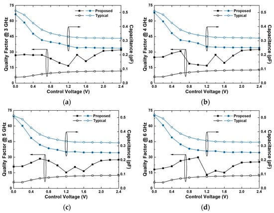
Figure 7.
Measured quality factor and capacitance of typical and proposed varactors: (a) 3 GHz, (b) 4 GHz, (c) 5 GHz, and (d) 6 GHz.
5. Conclusions
In this study, we proposed a layout technique of the MOS varactors for cross-coupled VCO applications. First, the effect on the quality factor of the metal line for the MOS varactor was analyzed. In order to improve the quality factor by mitigating the parasitic components of the metal line for the typical MOS varactor structures, the metal line for connecting the two MOS varactors was removed by combining the two MOS varactors for the typical cross-coupled VCO into one MOS varactor. The proposed MOS varactor structure consisted of several MOS transistors in the finger type, and all of the drains and sources of the fingers were connected to each other to form a single node, through which a control voltage for varying the capacitance of the MOS varactor was applied. On the other hand, gates that were not adjacent to each other were connected to each other, and the proposed MOS varactor had a total of two gate nodes. These two gate nodes were connected to the differential nodes of the differential cross-coupled VCO, respectively. To verify the feasibility of the proposed MOS varactor structure, the typical and proposed MOS varactors were designed using a 180 nm RFCMOS process. Compared to the typical structure, it was confirmed that the proposed structure had a reduced chip area by approximately 32%. In addition, it was confirmed through measurements that the parasitic capacitance induced by the interconnection metal line which was essential in the typical MOS varactor structure was successfully removed. Finally, regardless of the control voltage of the MOS varactor, it was confirmed that the MOS varactor with the proposed structure had a higher quality factor than that of the typical structure.
Author Contributions
Conceptualization, M.L. and C.P.; methodology, M.L., J.L., and C.P.; investigation, M.L.; supervision, C.P.; writing—original draft, M.L. and J.L.; review and editing, C.P. All authors have read and agreed to the published version of the manuscript.
Funding
This work was supported by the Development of Civil Military Technology Project by the Institute of Civil Military Technology Cooperation (ICMTC) under grant 21-CM-RA-02.
Data Availability Statement
All of the materials used in the study are mentioned within the article.
Conflicts of Interest
The authors declare no conflict of interest.
References
- Hamidi, S.B.; Dawn, D. A 2-Bit Voltage-Controlled Oscillator (VCO) for Multiband Wireless Applications. IEEE Microw. Wirel. Compon. Lett. 2022, 32, 1307–1310. [Google Scholar] [CrossRef]
- Wan, C.; Xu, T.; Yi, X.; Xue, Q. A VCO with Extra Cross-Coupling Path. IEEE Microw. Wirel. Compon. Lett. 2021, 31, 1130–1133. [Google Scholar] [CrossRef]
- Butryn, I.; Siwiec, K.; Pleskacz, W.A. Hybrid Cross Coupled Differential Pair and Colpitts Quadrature Digitally Controlled Oscillator Architecture. Electronics 2021, 10, 1132. [Google Scholar] [CrossRef]
- Deng, X.; Tan, P. An Ultra-Low-Power K-Band 22.2 GHz-to-26.9 GHz Current-Reuse VCO Using Dynamic Back-Gate-Biasing Technique. Electronics 2021, 10, 889. [Google Scholar] [CrossRef]
- Yook, B.; Park, K.; Park, S.; Lee, H.; Kim, T.; Park, J.S.; Jeon, S. A CMOS W-Band Amplifier with Tunable Neutralization Using a Cross-Coupled MOS–varactor Pair. Electronics 2019, 8, 537. [Google Scholar] [CrossRef]
- Maiellaro, G.; Caruso, G.; Scaccianoce, S.; Giacomini, M.; Scuderi, A. 40 GHz VCO and Frequency Divider in 28 nm FD-SOI CMOS Technology for Automotive Radar Sensors. Electronics 2021, 10, 2114. [Google Scholar] [CrossRef]
- Yelleswarapu, P.; Jha, A.; Willis, R.; Makris, Y.; Kenneth, K.O. Phase Noise Reduction in LC VCO’s Using an Array of Cross-Coupled Nanoscale MOSFETs and Intelligent Post-Fabrication Selection. IEEE Trans. Microw. Theory Tech. 2022, 70, 3244–3256. [Google Scholar] [CrossRef]
- Mansour, I.; Mansour, M.; Aboualalaa, M.; Allam, A.; Abdel-Rahman, A.B.; Pokharel, R.K.; Abo-Zahhad, M. Ku-Band Low Phase Noise VCO Using High-Quality Factor Transformer in 0.18-μm CMOS Technology. IEEE Microw. Wirel. Compon. Lett. 2022, 32, 1207–1210. [Google Scholar] [CrossRef]
- Mansour, I.; Mansour, M.; Aboualalaa, M.; Allam, A.; Abdel-Rahman, A.B.; Pokharel, R.K.; Abo-Zahhad, M. Dual-Band VCO Using High Quality Factor Two Orthogonally Located Inductors in 0.18-μm CMOS Technology. IEEE Microw. Wirel. Compon. Lett. 2022, 32, 1431–1434. [Google Scholar] [CrossRef]
- Hajimiri, A.; Lee, T.H. A General Theory of Phase Noise in Electrical Oscillators. IEEE J. Solid-State Circuit 1998, 33, 179–194. [Google Scholar] [CrossRef]
- Wagner, E.; Shana’a, O.; Rebeiz, G.M. A Very Low Phase-Noise Transformer-Coupled Oscillator and PLL for 5G Communications in 0.12 μm SiGe BiCMOS. IEEE Trans. Microw. Theory Tech. 2020, 68, 1529–1541. [Google Scholar] [CrossRef]
- Jahan, N.; Barakat, A.; Pokharel, R.K. Design of Low Phase Noise VCO Considering C/L Ratio of LC Resonator in 0.18-μm CMOS Technology. IEEE Trans. Circuits Syst. II Express Briefs 2021, 68, 3513–3517. [Google Scholar] [CrossRef]
- Hejazi, A.; Pu, Y.; Lee, K.-Y. A Design of Wide-Range and Low Phase Noise Linear Transconductance VCO with 193.76 dBc/Hz FoMT for mm-Wave 5G Transceivers. Electronics 2020, 9, 935. [Google Scholar] [CrossRef]
- Quemerais, T.; Gloria, D.; Golanski, D.; Bouvot, S. High-Q MOS Varactors for Millimeter-wave Applications in CMOS 28-nm FDSOI. IEEE Electron Device Lett. 2015, 36, 87–89. [Google Scholar] [CrossRef]
- Ghorbani-Nejad, A.; Nabavi, A. A Technique for Enhancing Varactor’s Quality Factor in Millimeter-Wave Frequencies. IEEE Trans. Circuits Syst. II Exp. Briefs 2017, 64, 872–876. [Google Scholar] [CrossRef]
- Razavi, B. Design of Analog CMOS Integrated Circuits; Mc Graw Hill: New York, NY, USA, 2000. [Google Scholar]


Disclaimer/Publisher’s Note: The statements, opinions and data contained in all publications are solely those of the individual author(s) and contributor(s) and not of MDPI and/or the editor(s). MDPI and/or the editor(s) disclaim responsibility for any injury to people or property resulting from any ideas, methods, instructions or products referred to in the content. |
© 2023 by the authors. Licensee MDPI, Basel, Switzerland. This article is an open access article distributed under the terms and conditions of the Creative Commons Attribution (CC BY) license (https://creativecommons.org/licenses/by/4.0/).