Abstract
Increasingly more power electronic devices are being connected to DC microgrids, which reduces the inertia of a DC microgrid, and the DC bus voltage has poor resistance to disturbance. Adding a virtual DC motor control to the converter can effectively suppress the fluctuation of the DC bus voltage; however, due to the fixed inertia and damping parameters, the system cannot attain a good dynamic performance. On this basis, a two-parameter adaptive virtual DC motor control is proposed to realize flexible change both in terms of inertia and damping, which improves the stability of the DC bus, and the system has good dynamic performance under this control. To further improve the stability of DC bus voltage and the flexibility of the microgrid control, in this paper, a dual active bridge (DAB) DC–DC converter controlled by dual phase shift (DPS) is taken as the research object, a three-parameter adaptive virtual DC motor control strategy is proposed to realize the flexible adjustment of inertia, damping, and armature resistance at the same time, and meanwhile, optimize the backflow power and inductor current stress of the converter. Finally, simulation and experiment results show that the proposed three-parameter adaptive control strategy compares with the two-parameter adaptive control strategy, and it can further reduce DC bus voltage fluctuation and recovery time, which improve the stability of the DC bus and the dynamic performance of the system. The DC bus voltage fluctuation rate under the three-parameter adaptive control is reduced to 9%, and the voltage recovery time is only 0.18 s; the optimization strategy can also effectively reduce the backflow power and inductor current stress.
1. Introduction
With the development of PV, energy storage sources, and other distributed energy sources, the DC microgrid has gradually become the focus of attention in recent years because it has high power supply reliability and its transmission lines have low losses; the DC microgrid has made great progress in the fields of power generation, transmission, and distribution [1,2].
A distributed energy source needs a DC converter to connect with the DC bus, and the DAB DC converter stands out among many DC converter topologies because it has low switching loss, low voltage stress, and high power density [3,4,5]. DAB connects the distributed energy source and the DC bus as an interface, and it realizes the bidirectional flow of power between the distributed energy source and the DC bus [6]. In addition to being widely used in DC microgrids, instances in the literature [7,8,9,10,11] have used DAB DC converters as battery chargers to connect battery energy storage systems with a 270 V electric aircraft power distribution bus, and proposed a predicted peak-current-based fast response control in DAB control to improve the response speed of the system.
A DAB DC converter has three control modes: single-phase shift control (SPS), dual-phase shift control (DPS), and triple-phase shift control (TPS) [12]. SPS control is simple, but DAB has high backflow power and inductor current stress under SPS control, which leads to a converter with low efficiency. The TPS control has three phase shift ratios, so it is the most flexible control, and DAB has low backflow power and inductor current stress under TPS, but the model of TPS is so complex that we seldom put it to practical use. DPS control has less backflow power and inductor current stress compared with SPS, and the model of DPS is simpler than TPS; we can also optimize the backflow power and inductor current stress of the converter by algorithm under DPS [13]. Literature [14] proposes a new DAB modeling method, it uses the two-time scale discrete-type models, which segregates the dynamics of the DAB converter into fast and slow state variables, which eases the analysis of the DAB converter.
Electronic converters connect with the DC microgrid, which make the DC microgrid lack inertia and damping, so fluctuations in system power will affect the stability of the DC bus voltage [15], thus threatening the safety and stability of the DC microgrid [16,17,18]. In order to improve the stability of the DC bus, the literature [19] introduces a virtual capacitor at the DC side, which improves the stability of the DC bus by using the voltage of a capacitor that cannot suddenly change, but virtual capacitance cannot provide additional damping for the system. In the AC microgrid, virtual synchronous machine (VSG) control provides the AC grid additional inertia and damping, which AC frequency will not drastically change. Compared with VSG control in the AC grid, the literature [20,21,22] proposes the virtual DC motor control strategy (VDCM), where the mechanical rotation equation and armature equation of the DC motor are added to the control of the converter, which attributes the converter with external characteristics like a motor so it improves the stability of the DC bus; in [23,24], the authors use VDCM control to improve the voltage of a PV power generation system, but the inertia and damping coefficient of the system are constants in VDCM, and they cannot be adjusted according to the different states of the DC bus voltage, which leads to the system lacking good dynamic performance; in [25], the paper designs a variable voltage drop control loop, combined with VDCM control, which improves the sensitivity of voltage control, but this control cannot reduce the fluctuation value of the DC bus when disturbed. On this basis, the literature [26,27] analyzes the influences of inertia and damping on system stability in VDCM by building small signal models. Studies [28,29,30] propose two-parameter adaptive control of VDCM to realize the flexible change in inertia and damping, which improves the dynamic performance of the DC bus, but the optimization effect of the two-parameter adaptive VDCM is limited, and the influence of other parameters of VDCM control on DC bus stability is not analyzed in these papers.
Based on the above literature, in order to further improve the stability of the DC bus and dynamic performance of the DC system, in this paper, we take a DAB DC converter controlled by DSP as the research object and propose a three-parameter adaptive VDCM control, which realizes the flexible change in inertial, damping, and armature resistance; at the same time, we optimize the backflow power and inductor current stress of the converter to improve the efficiency of the converter.
The rest of the paper is organized as follows. In Section 2, the topology of DAB under DSP control is analyzed. In Section 3, the VDCM control is introduced into the converter, and a small signal model of DAB is built to analyze the influence of different armature resistance on the stability and dynamic performance of the DC bus, and the three-parameter adaptive VDCM control is proposed in this section. In Section 4, the setting and adjustment principles of armature resistance are analyzed. In Section 5, the backflow power and inductor current stress of the converter are optimized by constructing Lagrangian functions. Finally, the advantages of three-parameter adaptive VDCM control in improving the stability of DC bus are verified through simulation and experiments.
2. Dual Phase-Shift Control (DPS) Principle
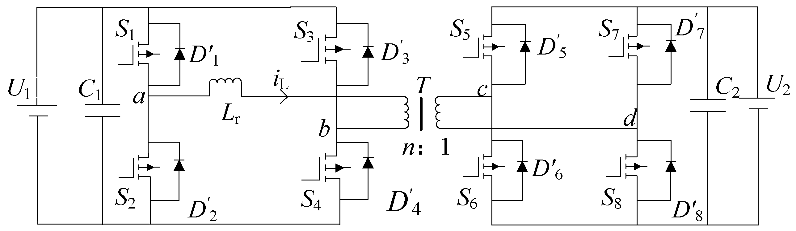
The topology of the DAB DC converter is shown in Figure 1, where U1, U2 represent the DC voltage on both sides, U1 can be the output voltage of distributed energy such as energy storage, U2 can be directly connected to the DC bus, n is the voltage ratio, Lr is the sum of the series inductance and leakage inductance at the primary side of the transformer, Lr is used to transfer power of DAB, C1 and C2 are capacitors for primary and secondary filtering and energy exchange, and are parasitic diodes on either side of the switch tube.

Figure 1.
DAB topology.
The working waveform is presented in Figure 2, where the upper and lower switch tubes of the same bridge arm are at 180° complementary conduction, is the half-switching period, is the current flowing through . The DPS control has a two phase-shift ratio, is the internal phase-shift ratio between , . is the external phase-shift ratio between , ; in this paper, we only analyze the condition that .
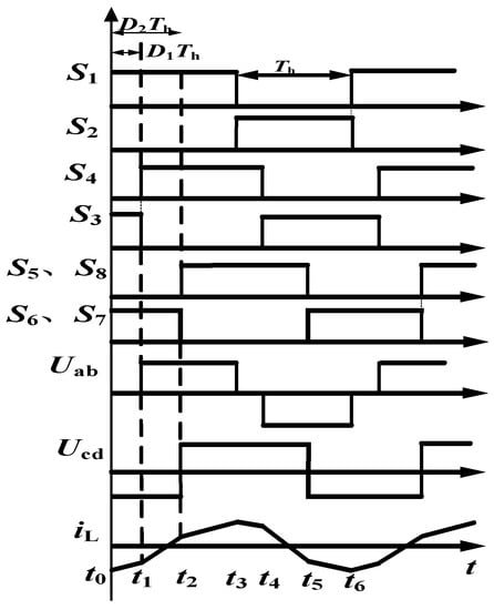
Figure 2.
Waveforms of DPS control.
3. VDCM Control
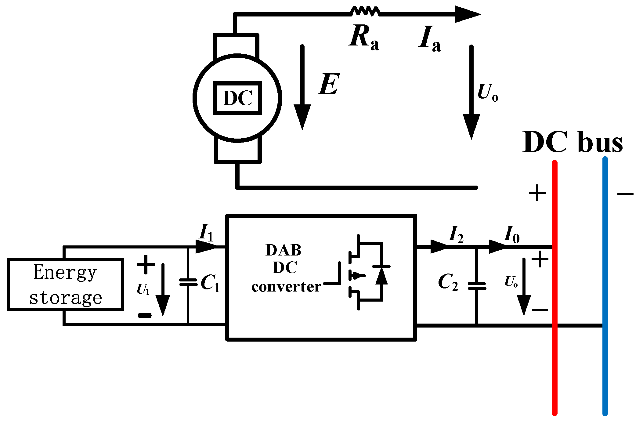
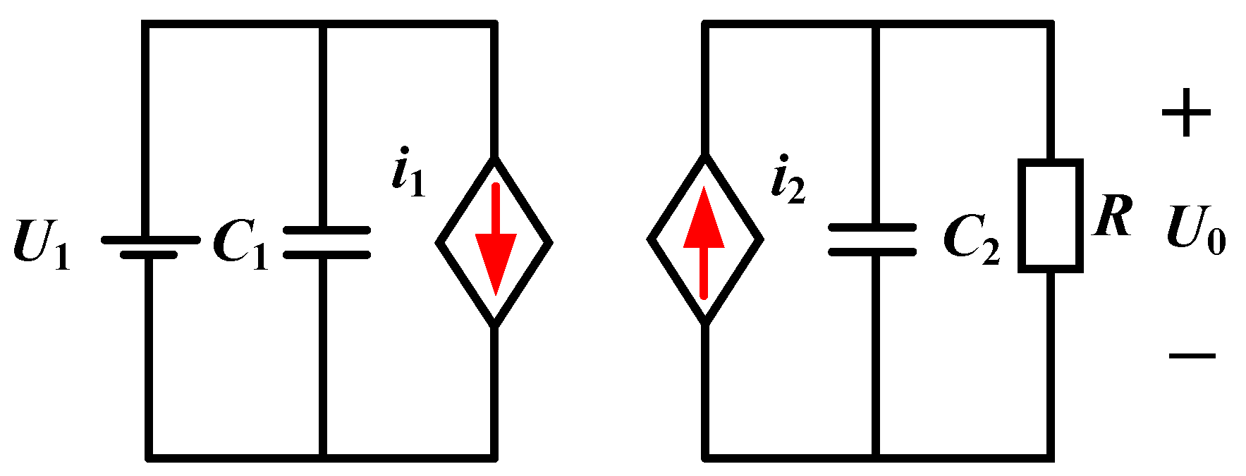
The DAB converter controlled by VDCM control is shown in Figure 3; the power side is supplied by the energy storage device.

Figure 3.
VDCM model.
are connected with the energy storage; they are the output voltage and the output current of the energy storage, and is the output current of the DAB DC converter, denote the DC bus voltage and DC bus current, is also the output voltage of the converter, and the mechanical rotation equation of the DC motor is shown in Formulas (1) and (2).
where J denotes the inertia constant, H denotes the damping coefficient of the DC motor, and are the actual rotational angular velocity and rated rotational angular velocity of the DC motor, respectively; are the mechanical torque and electromagnetic torque of the DC motor, are the input mechanical power and the output electromagnetic power of the DC motor, and the actual value of the DC bus voltage corresponds to the actual value of in the DC motor, and the rated value of the DC bus voltage corresponds to in the DC motor.
The armature equation of the DC motor can be expressed as:
where E is the armature electromotive force of the DC motor, it can be written as , where means flux per pole, denotes the torque coefficient, denotes the total equivalent resistance of the armature circuit, and denotes the armature current. The electromagnetic power of the DC motor can be written as .
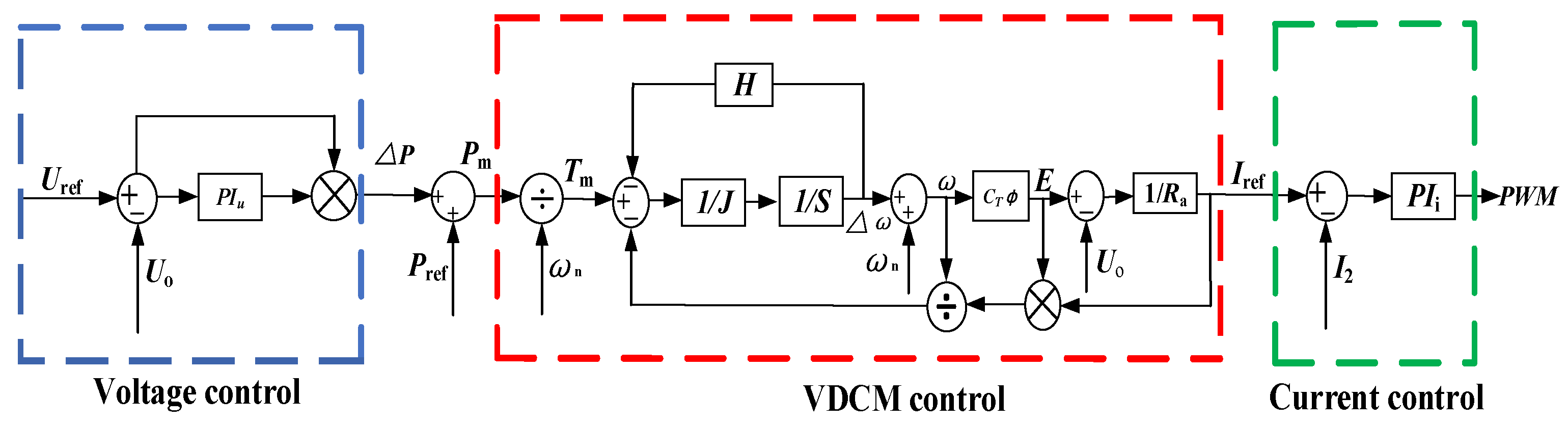
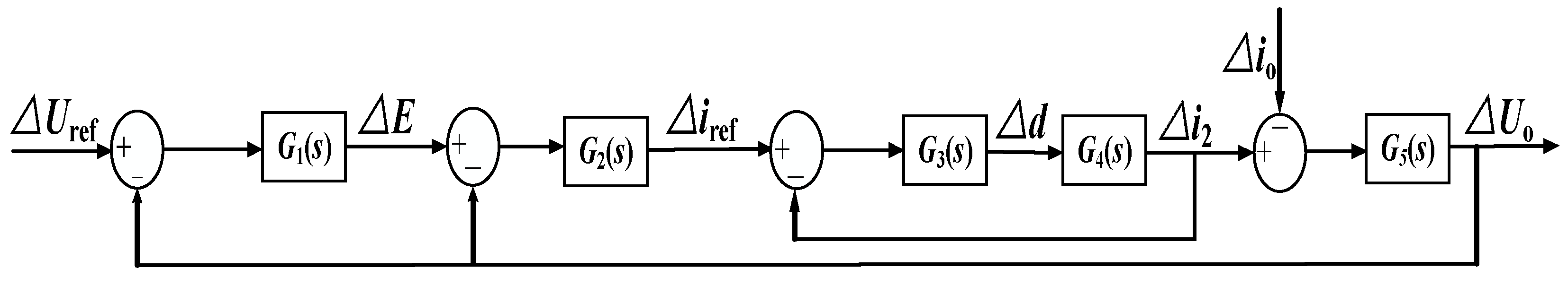
The control block diagram of the VDCM control strategy is shown in Figure 4, on the basis of the voltage loop and the current loop, adding the VDCM control loop. In the voltage control part, the DC bus voltage feedback value and the DC bus voltage reference value are compared, using the voltage proportional integral (PI) controller to adjust and obtain mechanical power deviation, and then add mechanical power reference value to obtain . In the VDCM control part, according to Formulas (1) and (3), which makes the converter operate as the DC motor to mimic its inertia characteristic, and then obtains the armature current ; is also the reference value of the output current of the converter. In the current control part, the output current feedback value and the output current reference value are compared using the current proportional integral (PI) controller to obtain PWM to control the operation of the switch tubes.

Figure 4.
Control block diagram of VDCM.
When , the converter works under SPS, and the SPS control only has one phase-shift ratio between . In DPS, determines the magnitude and direction of the transmitted power, in DPS and has the same effects with in SPS; therefore, DPS has a similar small signal model to SPS. We build a small signal model of SPS instead of DPS to simplify operation, and and are completely equivalent in the subsequent research.
The average model of the DAB DC converter is shown in Figure 5, and the transmitted power of the DAB under SPS can be expressed as (4) [31]; it can be seen that of the DAB converter is not only affected by the the input and , but it is also restricted by the n, D, and . Combined with Figure 3, the instantaneous value of and of the converter can be represented as (5) and (6):
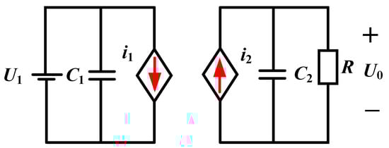
Figure 5.
Average model of DAB converter.
The small signal decomposition is carried out for each parameter in (6), and ignored for the change in to obtain Equation (7). and d denote steady state quantities of and D, and denote the small signal AC components of and D.
Ignoring the DC components and the second-order AC components in Equation (7), according to the Laplace transform, we can transform (7) into (8):
The transfer function of the VDCM control can be derived from Figure 4:
In order to analyze the stability of the whole system, which adopts VDCM control, combined with Figure 4, the small signal model of DAB is established in Figure 6, where stands for the change in each parameter.
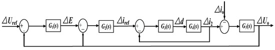
Figure 6.
Small signal model of DAB DC converter.
The following formula can be obtained from Figure 6, where are proportion and integral coefficient of the voltage loop, are proportion and integral coefficient of the current loop.
Adding the VDCM control to the converter, it is equivalent to introduce a first-order inertia link into the control of the converter [32], the amplitude margin and phase margin of the system are improved, thus improving the stability of the system; it is also equivalent to add a virtual capacitor in the DC bus side, and the voltage at both ends of the capacitor cannot be suddenly changed; thus, the VDCM control can suppress the fluctuation of the DC bus voltage.
According to Figure 6 and Equation (10), the open-loop transfer function from to can be expressed as :
The literature [33] has analyzed the influence of different values of J and H on system stability, so this paper only analyzes the influence of different values of armature resistance on system stability.
We change Equation (11) into Equation (12), and the value of affects both the second-order part a and the inertial part b of from Equation (12).
Defining :
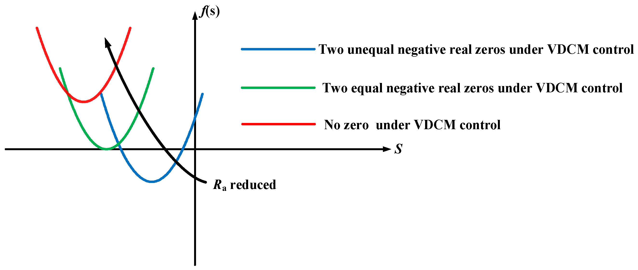
Assuming that and are zero points of , which , the change in the value of will make the zero points of change. The relation between the value of and the zero points of is shown in (14).
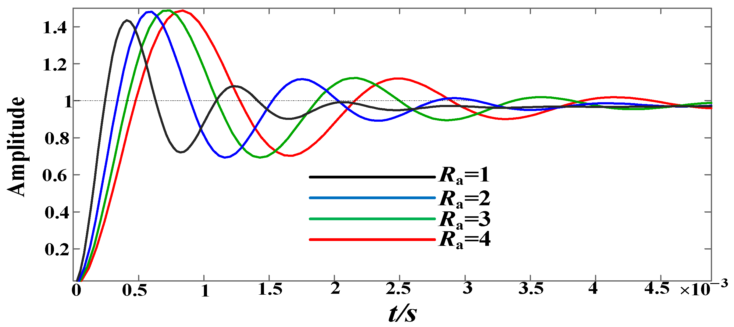
With the decreases in , the change trend of is shown in Figure 7; the change in zero points is two negative zero points, two equal zero points, and no zero points; the poles points change in the second-order part a in is two negative real pole points, two equal negative real pole points, and a pair of conjugate pole points. will increase as decreases, and the pole points of the second-order a in gradually move away from the real axis, which makes the system decay speed and response speed faster. The step response of under different is shown in Figure 8.
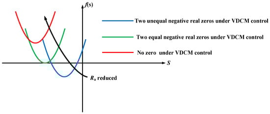
Figure 7.
under different .
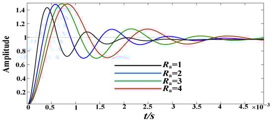
Figure 8.
Step response of under different .
We change Equation (11) into Equation (15), K is the open-loop gain of .
The open-loop gain K of can be expressed as:
It can be seen from (16) that K is irrelevant with J; it is directly proportional with the value of and inversely proportional with the value of H, and the time constant of the inertia link of Equation (15) is also directly proportional to . Comparing the position relationship between and J in Equation (15), they have the same influence on the inertia of the system, and the increase in can be equivalent to the increase in J.
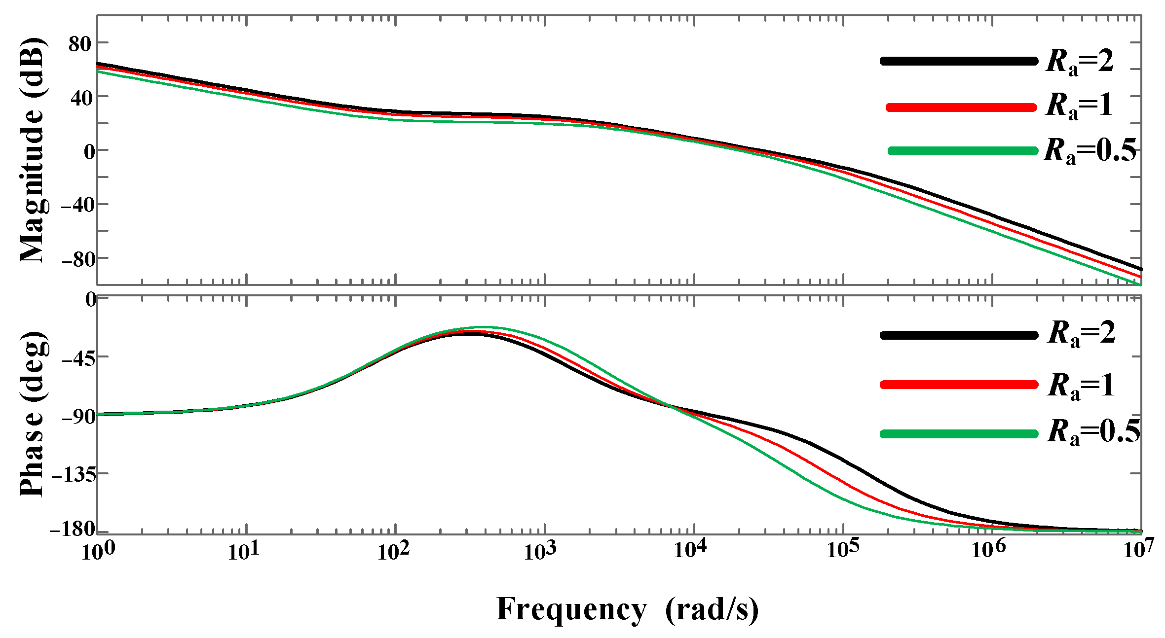
Based on the small signal model of the DAB DC converter, the open-loop Bode diagram of is drawn to analyze the influence of on the stability of the control system. The open-loop Bode diagram with different is shown in Figure 9, the phase angle margin and the open-loop gain K will increase as increases within a certain range.
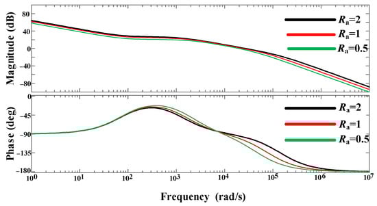
Figure 9.
Bode plots under different .
The transfer function from to in Figure 6 can be expressed as:
By drawing the unit step response curve of , we can simulate the change process of the DC bus voltage when disturbed by the load. The unit step response of for different values of is shown in Figure 10; it can be seen that when the converter is disturbed by the load, the output voltage has a larger deviation when the increases.
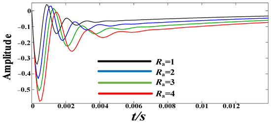
Figure 10.
Unit step response curves under different .
4. Three Parameter VDCM Adaptive Control
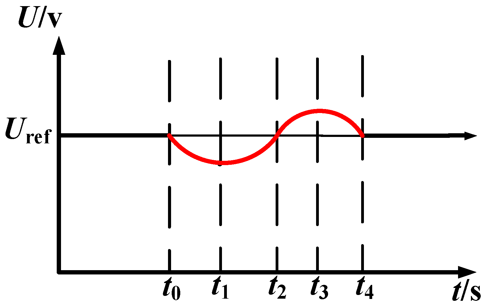
Taking the increase in output power of the converter as an example, the DC bus voltage is divided into several intervals, as shown in Figure 11; when the deviates from the , we need a smaller to reduce the voltage deviation and speed up the response of the system. When the output voltage returns to the , we need a larger to provide additional inertia for the system. The literature [34] analyzed how to choose and H in different voltage intervals. Table 1 shows the selection of three parameters, where , and are inertia, damping, and the armature resistance coefficient when the system is stable.
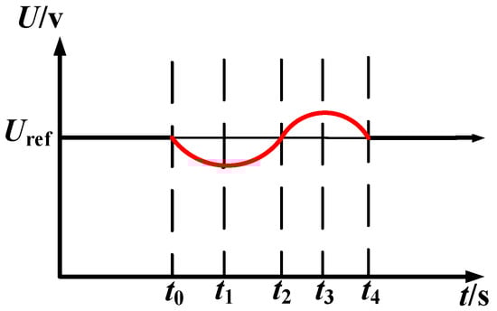
Figure 11.
Output voltage curve of the converter when disturbed.

Table 1.
Values of J, H, and .
The adaptive regulation of three parameters can be realized by (18), (19), and (20), where c denotes the DC bus voltage change threshold, when the DC bus change exceeds the threshold, and the converter enters the VDCM adaptive adjustment mode; is the difference between the reference value and the actual value , and x is the rate of change in the DC bus voltage; A, B, and F are the regulating coefficients of J, H, and .
From 0 to , the system remains stable, the DC bus voltage is , , and the armature resistance is . From to , the load power suddenly increases, and at this time , , is reduced to enhance the system response speed, and reduce the fluctuation of . From to , the DC bus voltage begins to recover to the , , is increased to increase the inertia of the system. From to , , we still use the smaller to reduce the voltage deviation of the DC bus. From to , , we use the larger to increase the inertia of the system, which makes the change in the DC bus voltage more gradual. J and H have the same adjustment principles as [35].
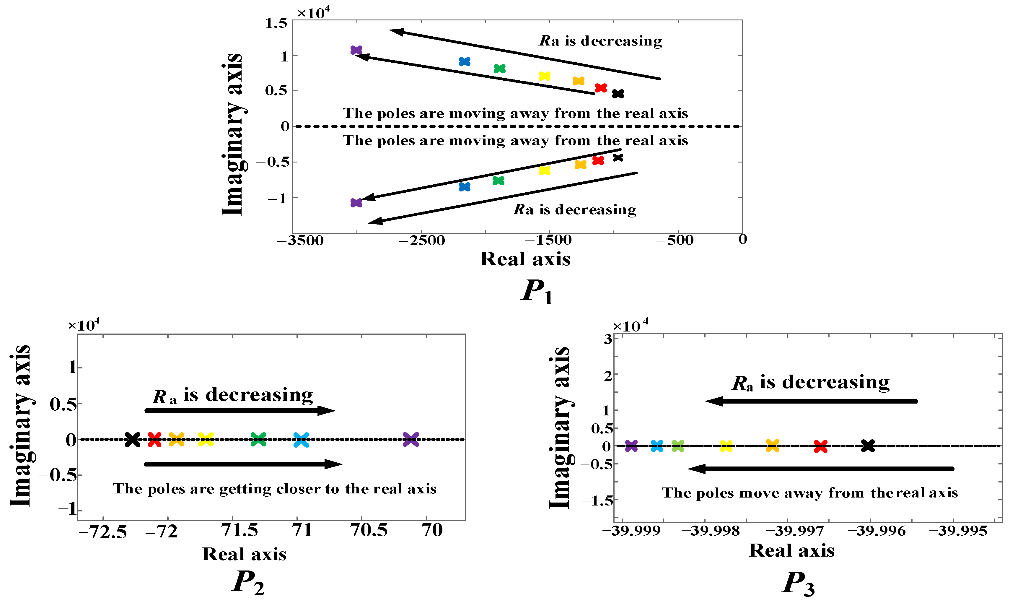
The design principles of , A, , and B have been detailed in the literature [35], so this paper mainly analyzes the selection principles of and . The closed-loop transfer function G of is as follows:
Drawing the zero-pole distribution diagram of G under and , G has four poles, and we divide the poles into three groups, and , as shown in Figure 12. is a pair of conjugate poles, and the real part of a pole is much larger than the other two groups, so it has the least influences on the system. Compared with , the real part of changes more with changes. As the dominant pole, has the greatest influence on the stability of the converter. After analyzing the influence of different poles on the system, we make and , the adjustment range of is 0.5~2, such that and .
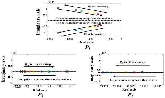
Figure 12.
Pole distribution of G under different .
5. Optimization of Backflow Power and Inductor Current Stress
Internal backflow power and inductor current stress determine the efficiency of DAB, so it is necessary to optimize backflow power and inductor current stress of the converter to reduce the loss of the converter.
In this paper, backflow power and inductor current stress of the converter are optimized by constructing the Lagrange function [36].
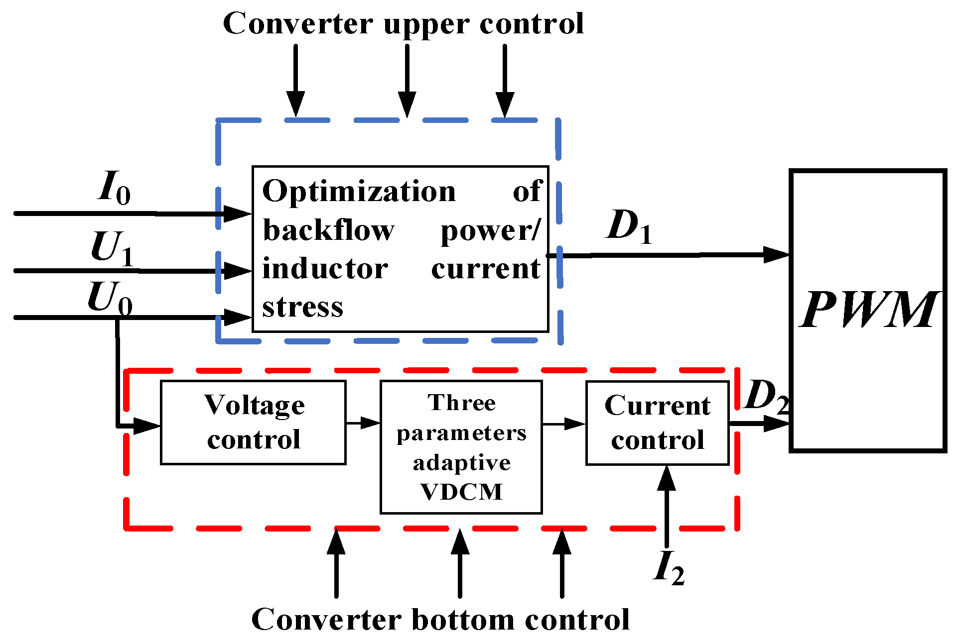
6. Integrated Control Strategy for Converter
In the DPS control, combined with Figure 3, is obtained by the upper control to improve the efficiency of the converter, and is obtained by the bottom control to improve the stability of the DC bus voltage, as shown in Figure 13.
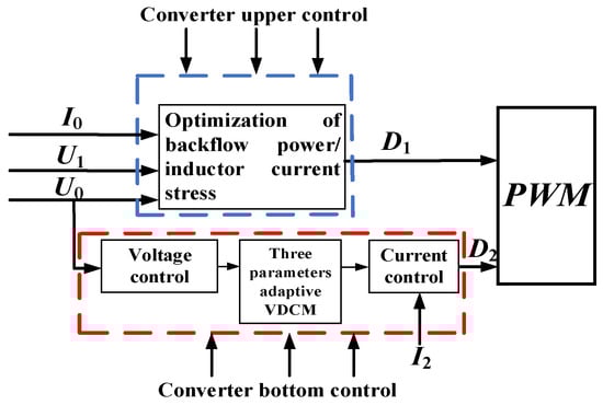
Figure 13.
Converter control block diagram.
7. Simulation and Analysis
MATLAB/Simulink simulation platform is used to verify the effectiveness of the control strategy. The secondary power supply is replaced by resistance R, and the voltage of R is the DC bus voltage ; related parameters are shown in Table 2.
Table 2.
Simulation parameters.
The initial voltage is maintained at 15 V before 0.2 s, at 0.2 s, the load R is reduced from 5 Ω to 2 Ω, and the load power increases from 45 W to 112.5 W; the DC bus voltage is shown in Figure 14.
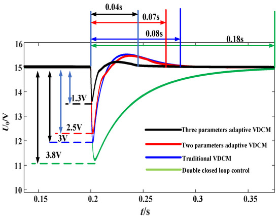
Figure 14.
DC bus voltage under different control strategies.
Under different control strategies, the fluctuation peak and recovery time of output voltage are shown in Table 3.
Table 3.
Fluctuation peak and recovery time of under different control strategies.
From Figure 14 and Table 3, the DC bus voltage has the smallest fluctuation peak and the shortest time to recover to steady-state value under the three-parameter adaptive VDCM.
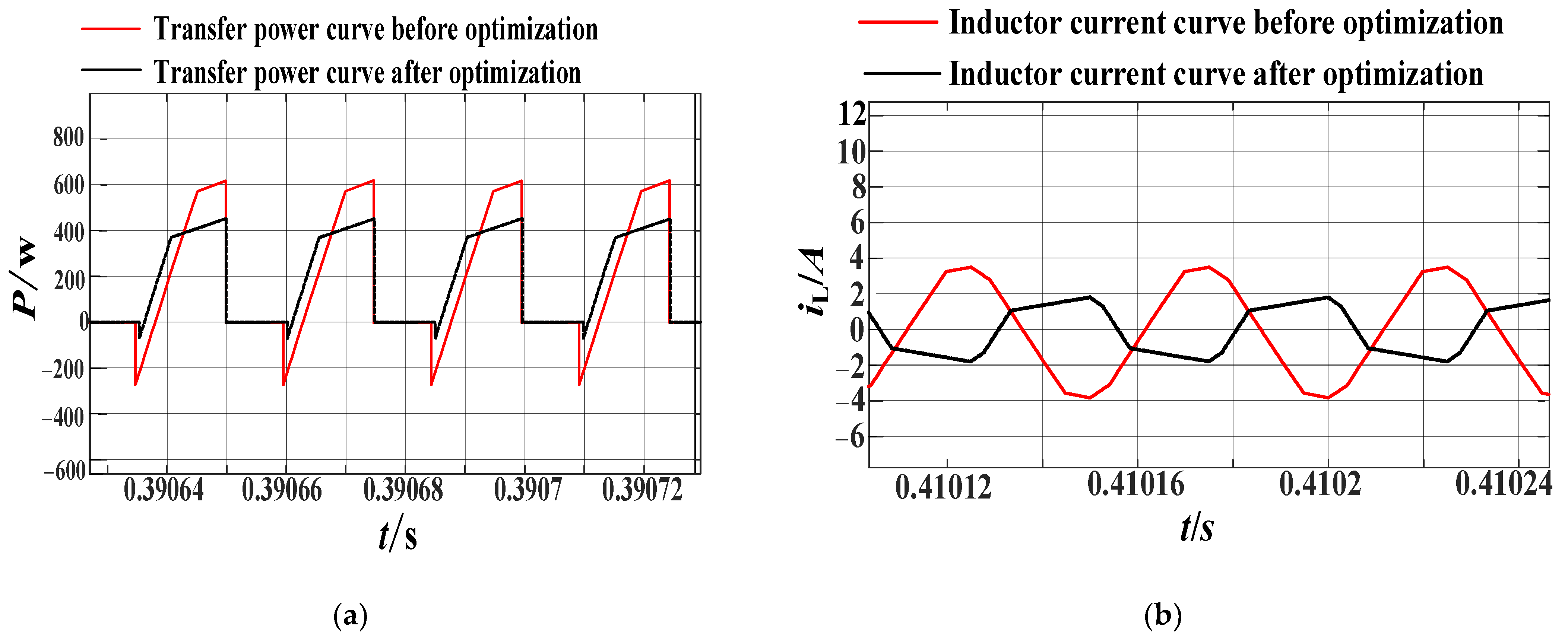
The instantaneous power and inductor current of the converter are shown in Figure 15.
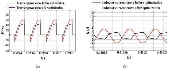
Figure 15.
Power/inductor current curve of the converter: (a) power curve; (b) inductor current curve.
The peak of backflow power is shown in Table 4, and the backflow power of the converter is obviously reduced after backflow power optimization.
Table 4.
Backflow power of converter.
The inductor current stress is shown in Table 5, and the inductor current stress of the converter is obviously reduced after inductance current stress optimization.
Table 5.
Inductor current stress of converter.
One thing to note is that adding VDCM control will not affect the backflow power and the inductor current stress of the converter. When adding the backflow power or inductance current stress optimization to the upper control of the converter, and are fixed, the bottom control will not change the size of , and different control strategies only affect the peak value of DC bus voltage fluctuation and the recovery time.
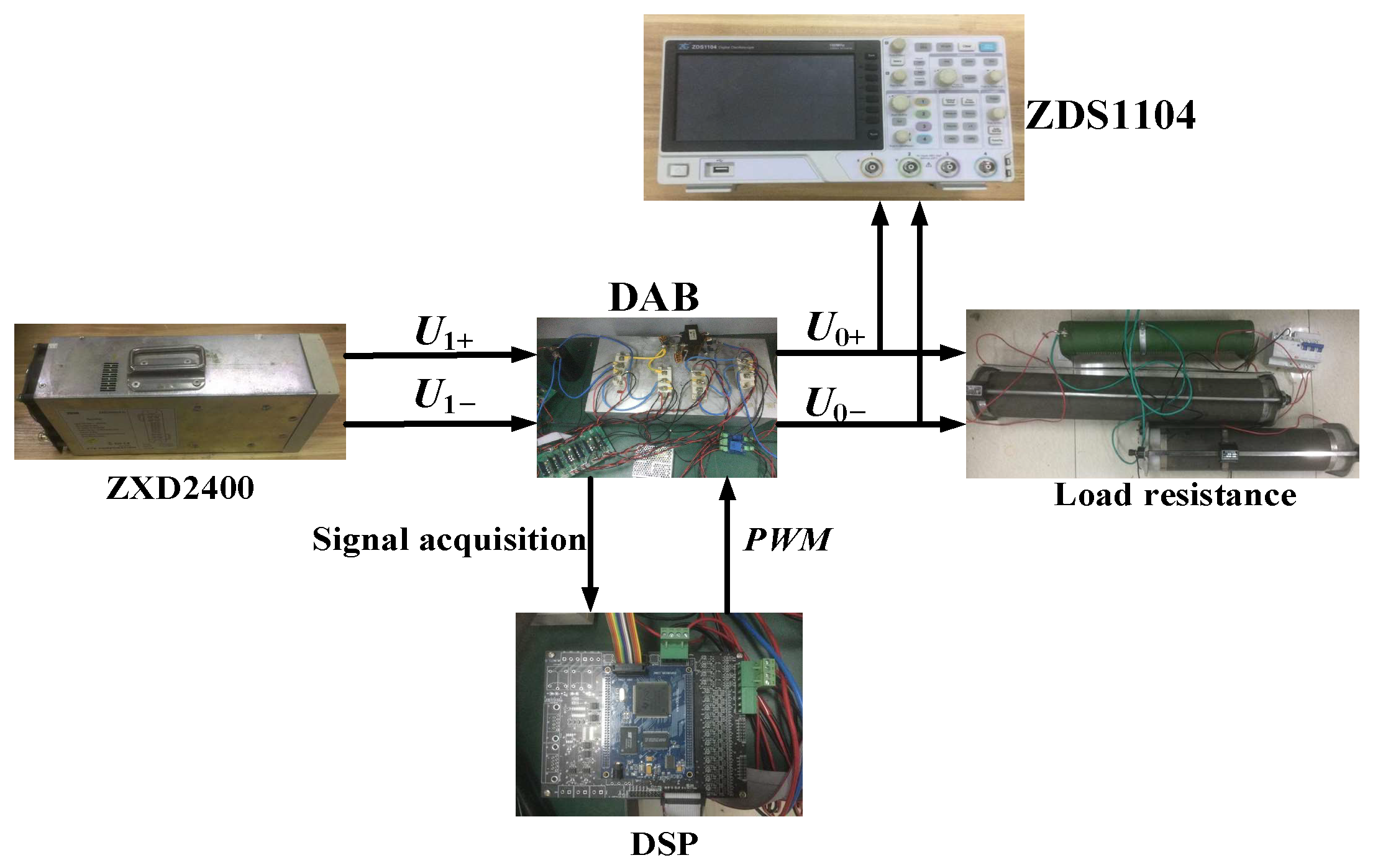
8. Experimental Verification
To further verify the effectiveness of the proposed control strategy, we constructed a DAB experimental platform, as shown in Figure 16. The DC power supply used ZXD2400, the DSP control board was used as the controller using a ZDS1104 oscilloscope to record the relevant waveforms. Due to the limited conditions of the experimental platform, the input voltage was set to 40 V during the experiment, the output voltage was 15 V, and we used an air switch to switch the load resistance to simulate load disturbances.
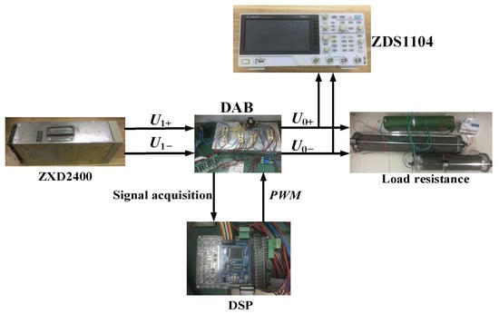
Figure 16.
Output voltage of the converter under different control strategies.
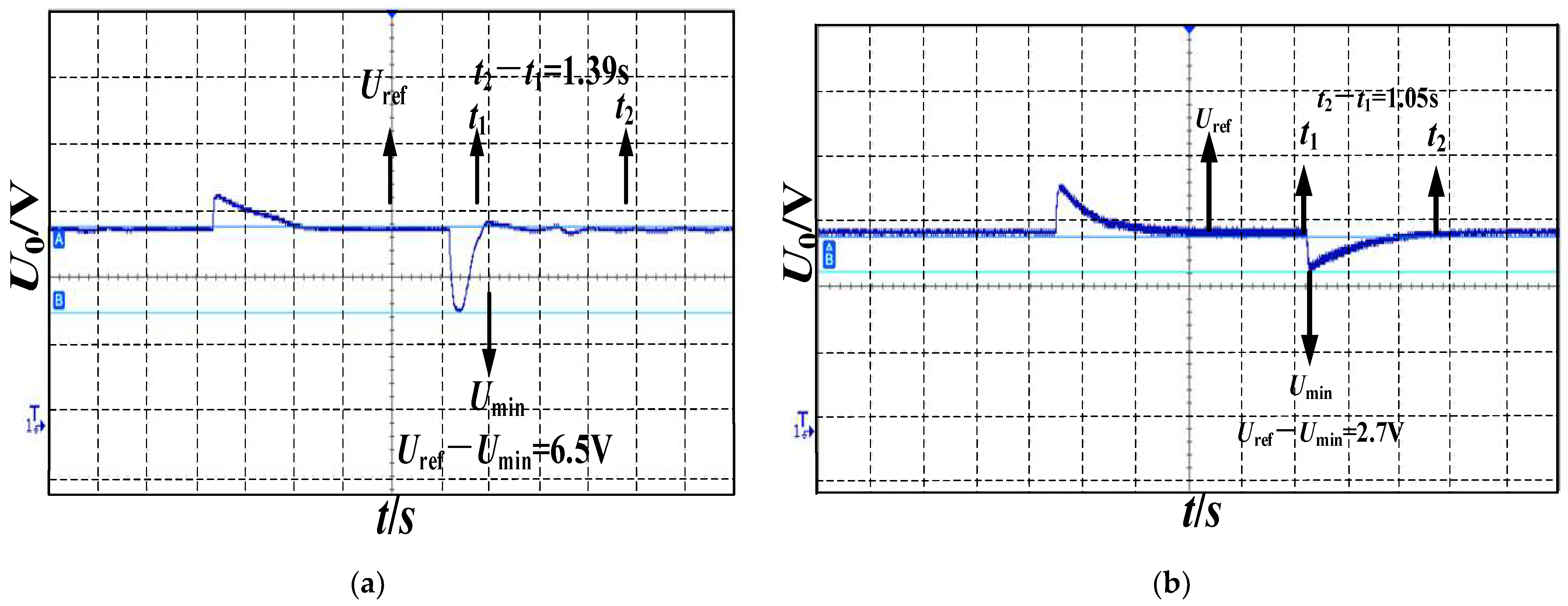
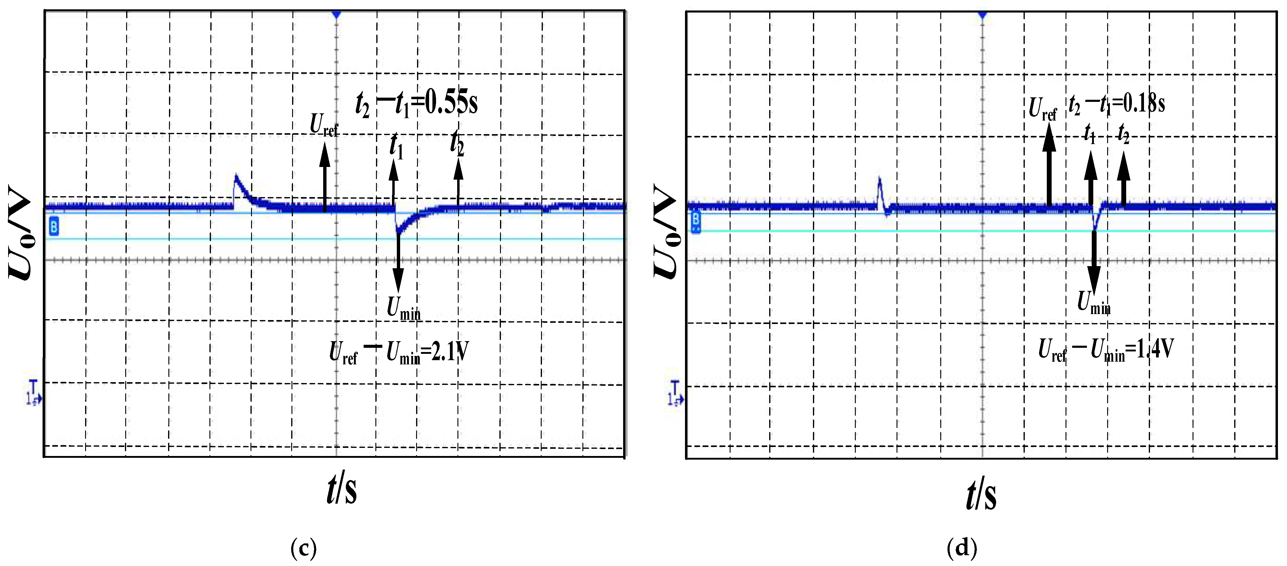
When the load resistance suddenly changed, the output voltage of the DAB under different control strategies is shown in Figure 17. We only analyzed the voltage change when the load resistance decreases.
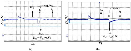
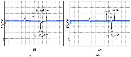
Figure 17.
Output voltage of the DAB under different control strategies: (a) traditional double closed-loop control; (b) traditional VDCM control; (c) J and H adaptive VDCM control; (d) J, H, and adaptive VDCM control.
is the minimum value of the output voltage, under different control strategies, and the fluctuation peak and recovery time of output voltage are shown in Table 6; we can see the DC bus voltage has the smallest fluctuation peak and the shortest recovery time under three-parameters adaptive VDCM from Table 6.
Table 6.
Fluctuation peak and recovery time of under different control strategies.
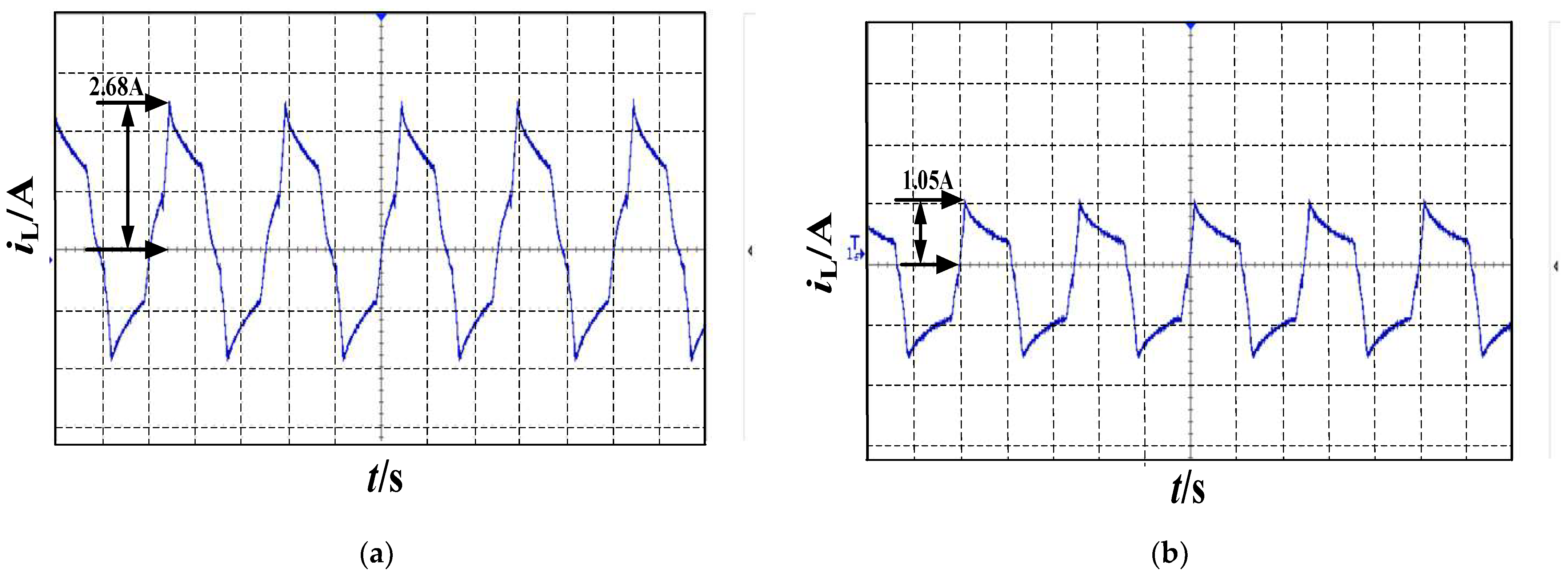
The inductor current waveforms of the converter before and after inductor current stress optimization are shown in Figure 18a,b.
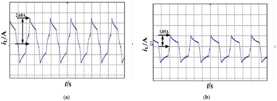
Figure 18.
Inductor current waveforms: (a) inductor current waveform before inductor current stress optimization; (b) inductor current waveform after inductor current stress optimization.
We can see the inductor current stress of the converter can be reduced after inductor current stress optimization from Table 7.
Table 7.
Inductor current stress of converter.
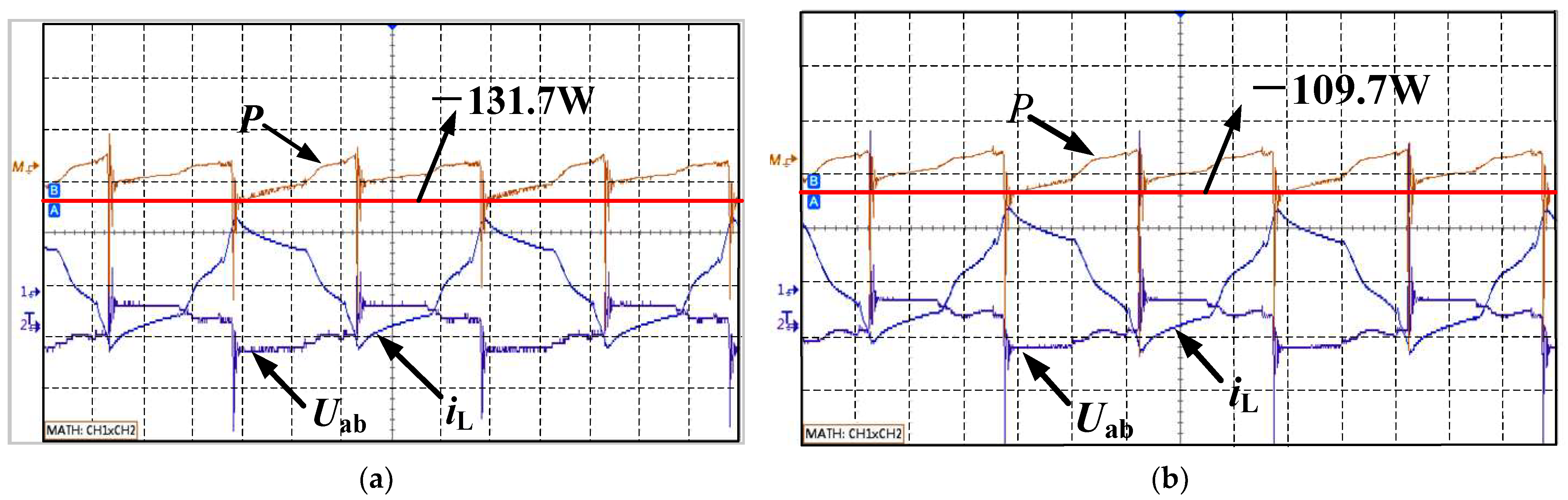
Before and after the backflow power optimization, the transmitted power P of the converter is shown in Figure 19a,b; P is the product of inductor current and primary side voltage of transformer , .
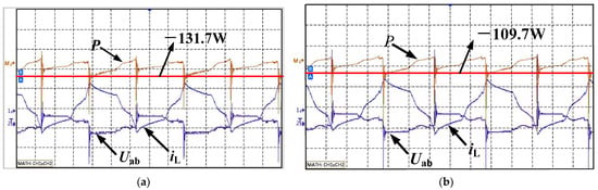
Figure 19.
Instantaneous power waveforms: (a) instantaneous power waveform of converter before backflow power optimization; (b) instantaneous power waveform of converter after backflow power optimization.
We can see the backflow power of the converter can be reduced after backflow power stress optimization from Table 8.
Table 8.
Backflow power of converter.
9. Conclusions
This paper proposes a three-parameter adaptive VDCM control strategy, which realizes the flexible adjustment of inertia, damping, and armature resistance, and this control strategy can further improve the stability of the DC bus voltage and the dynamic performance of the system; at the same time, the backflow power and inductor current stress are optimized to improve the efficiency of the converter. The results, which are obtained from simulations and experiments, prove the superiority of the three-parameter adaptive VDCM control, and this control can reduce the fluctuation rate of the DC bus voltage from 14% to 9%, and reduce the recovery time of the DC bus voltage from 0.55 s to 0.18 s.
Because the number of adaptive parameters increases, it may lead to the oscillation of the DC bus voltage, and how to choose the appropriate filtering methods to reduce the ripple of the DC bus voltage is something that we need to study in the future.
Author Contributions
Methodology, W.K.; Software, Y.W.; Data curation, L.C.; Writing—review and editing, L.Z. All authors have read and agreed to the published version of the manuscript.
Funding
This research was funded by the National Natural Science Foundation of China, China grant number [52241702]; Study on Constraint factors and evaluation method of new energy flexible direct transmission System, grant number [HX20210517].
Data Availability Statement
The data presented in this study are available in the text.
Conflicts of Interest
The authors declare no conflict of interest.
References
- Sharma, S.; Iyer, V.M.; Bhattacharya, S.; Kikuchi, J.; Zou, K. Tertiary Control Method for Droop Controlled DC-DC converters in DC Microgrids. In Proceedings of the 2021 IEEE Energy Conversion Congress and Exposition (ECCE), Vancouver, BC, Canada, 10 October 2021; pp. 694–699. [Google Scholar] [CrossRef]
- Zhuang, X.; Zhang, Q.; Liu, Y.; Zhu, P.; Zeng, Y. Asynchronous Startup of the Paralleled DC-DC Converters in DC Microgrid Based on the Injected Frequency. In Proceedings of the 2021 5th International Conference on Green Energy and Applications (ICGEA), Singapore, 6 March 2021; pp. 63–68. [Google Scholar] [CrossRef]
- Zhao, B.; Song, Q.; Liu, W.; Sun, Y. Overview of Dual-Active-Bridge Isolated Bidirectional DC–DC Converter for High-Frequency-Link Power-Conversion System. IEEE Trans. Power Electron. 2014, 298, 4091–4106. [Google Scholar] [CrossRef]
- Le, T.-T.; Nguyen, M.-K.; Wang, C.; Choi, S. Fault-Tolerant Control of Three-Phase Bidirectional Current-Fed Dual Active Bridge DC-DC Converter. In Proceedings of the 2021 IEEE Transportation Electrification Conference & Expo (ITEC), Chicago, IL, USA, 21 June 2021; pp. 360–363. [Google Scholar] [CrossRef]
- Wen, J.; Wen, H.; Bu, Q. An Optimal Control for Dual-Active-Bridge DC-DC Converter in Eliminating Transient DC Bias Current. In Proceedings of the 2019 IEEE 10th International Symposium on Power Electronics for Distributed Generation Systems (PEDG), Xi’an, China, 3–6 June 2019; pp. 849–852. [Google Scholar] [CrossRef]
- Esteban, F.D.; Serra, F.M.; de Angelo, C.H. Control of a DC-DC Dual Active Bridge Converter in DC Microgrids Applications. IEEE Lat. Am. Trans. 2021, 19, 1261–1269. [Google Scholar] [CrossRef]
- Tariq, M.; Maswood, A.I.; Gajanayake, C.J.; Gupta, A.K. Modeling and Integration of a Lithium-Ion Battery Energy Storage System with the More Electric Aircraft 270 V DC Power Distribution Architecture. IEEE Access 2018, 6, 41785–41802. [Google Scholar] [CrossRef]
- Tariq, M.; Maswood, A.I.; Gajanayake, C.J.; Gupta, A.K.; Sasongko, F. Battery energy storage system integration to the more electric aircraft 270 V DC power distribution bus using peak current controlled dual active bridge converter. In Proceedings of the 2017 IEEE Energy Conversion Congress and Exposition (ECCE), Cincinnati, OH, USA, 1–5 October 2017; pp. 2068–2073. [Google Scholar] [CrossRef]
- Tariq, M.; Maswood, A.I.; Gajanayake, C.J.; Gupta, A.K. Modeling of a Li-ion battery energy storage system using an optimal harmonic number based model of DC-DC converter for more electric aircraft. In Proceedings of the IECON 2016—42nd Annual Conference of the IEEE Industrial Electronics Society, Florence, Italy, 23–26 October 2016; pp. 4429–4434. [Google Scholar] [CrossRef]
- Tariq, M.; Maswood, A.I.; Gajanayake, C.J.; Gupta, A.K. A Lithium-ion battery energy storage system using a bidirectional isolated DC-DC converter with current mode control for More Electric Aircraft. In Proceedings of the 2016 IEEE Symposium on Computer Applications & Industrial Electronics (ISCAIE), Penang, Malaysia, 30–31 May 2016; pp. 149–154. [Google Scholar] [CrossRef]
- Tariq, M.; Maswood, A.I.; Gajanayake, C.J.; Ooi, G.H.P.; Chatterjee, P.; Madishetti, S.; Molligoda, D.A.; Gupta, A.K. Battery integration with more electric aircraft DC distribution network using phase shifted high power bidirectional DC-DC converter. In Proceedings of the 2015 IEEE PES Asia-Pacific Power and Energy Engineering Conference (APPEEC), Brisbane, Australia, 15–18 November 2015; pp. 1–5. [Google Scholar] [CrossRef]
- Jin, L.; Liu, B.; Duan, S. ZVS operation range analysis of three-level dual active bridge DC-DC converter with phase-shift control. In Proceedings of the 2017 IEEE Applied Power Electronics Conference and Exposition (APEC), Tampa, FL, USA, 26–30 March 2017; pp. 362–366. [Google Scholar] [CrossRef]
- Bu, Q.; Wen, H.; Wen, J. Optimized Transient Modulation Control of Bidirectional Full-Bridge DC-DC Converter. In Proceedings of the 2019 10th International Conference on Power Electronics and ECCE Asia (ICPE 2019—ECCE Asia), Busan, Korea, 27–31 May 2019; pp. 3102–3107. [Google Scholar] [CrossRef]
- Iqbal, M.T.; Maswood, A.I.; Tariq, M.; Iqbal, A.; Verma, V.; Urooj, S. A Detailed Full-Order Discrete-Time Modeling and Stability Prediction of the Single-Phase Dual Active Bridge DC-DC Converter. IEEE Access 2022, 10, 31868–31884. [Google Scholar] [CrossRef]
- Liao, J.; Zhou, N.; Wang, Q.; Li, C.; Yang, J. Definition and Correlation Analysis of Power Quality Index of DC Distribution Network. Proc. CSEE 2018, 38, 6847–6860. [Google Scholar]
- Zhu, X.R.; Meng, F.Q. Stability Analysis of DC Microgrid with Virtual Inertia Control. Power Syst. Technol. 2020, 44, 208–218. [Google Scholar] [CrossRef]
- Zhao, B.; Yu, Q.G.; Sun, W.X. Extended-Phase-Shift Control of Isolated Bidirectional DC-DC Converter for Power Distribution in Microgrid. IEEE Trans. Power Electron. 2012, 2711, 4667–4680. [Google Scholar] [CrossRef]
- Zhu, X.R.; Xie, Z.Y.; Jing SZ Jing, S. Virtual Inertia Control and Stability Analysis of DC Micro-Grid. Power Syst. Technol. 2017, 41, 3884–3893. [Google Scholar] [CrossRef]
- Unamuno, E.; Barrena, J. Design and small-signal stability analysis of a virtual-capacitor control for DC microgrids. In Proceedings of the 19th European Conference on Power Electronics and Application, Warsaw, Poland, 11–14 September 2017. [Google Scholar]
- Bagheri, S.; CheshmehBeigi, H.M. DC Microgrid Voltage Stability through Inertia Enhancement Using a Bidirectional DC-DC Converter. In Proceedings of the 7th Iran Wind Energy Conference (IWEC2021), Shahrood, Iran, 17 May 2021; pp. 1–5. [Google Scholar] [CrossRef]
- Guo, Y.; Ma, W.; Meng, J.; Wang, Y. A Virtual Inertia Control Strategy for Dual Active Bridge DC-DC Converter. In Proceedings of the 2018 2nd IEEE Conference on Energy Internet and Energy System Integration (EI2), Beijing, China, 20–22 October 2018; pp. 1–5. [Google Scholar] [CrossRef]
- Soumya, S.; Prakash, M.J.; Krishna, R.B. Virtual DC machine: An inertia emulation and control technique for a bidirectional DC-DC converter in a DC microgrid. IET Electr. Power Appl. 2018, 126, 874–884. [Google Scholar]
- Cheng, Q.; Yang, X.; Chu, S.; Zhang, Q.; Huang, S. Research on Control Strategy of PV System Based on Virtual DC Generator. High Volt. Eng. 2017, 47, 2097–2104. [Google Scholar]
- Zhang, H.; Tan, S.; Xiao, X.; Zhi, N. Control Strategy of Energy Storage Converter with DC Machine Characteristics. High Volt. Eng. 2018, 44, 119–125. [Google Scholar]
- Zhang, X.; Li, H.; Fu, Y. Optimized Virtual DC Machine Control for Voltage Inertia and Damping Support in DC Microgrid. In Proceedings of the 2021 IEEE Applied Power Electronics Conference and Exposition (APEC), Phoenix, AZ, USA, 14–17 June 2021; pp. 2727–2732. [Google Scholar] [CrossRef]
- Neves, M.S.; Alves, F.A.L.; Aredes, M.A.; Costa, J.A.V.C.; Aredes, M. A Virtual DC Machine Control Strategy with Nonlinear Behavior to Enhance Power Sharing and Voltage Regulation in DC Microgrids. In Proceedings of the 2021 IEEE Fourth International Conference on DC Microgrids (ICDCM), Arlington, VA, USA, 18 July 2021; pp. 1–8. [Google Scholar] [CrossRef]
- Zhi, N.; Ding, Y.; Du, L. Virtual DC Generator Control Strategy Based on Differential Compensation. In Proceedings of the 2019 IEEE Energy Conversion Congress and Exposition (ECCE), Baltimore, MD, USA, 29 September–3 October 2019; pp. 1454–1458. [Google Scholar] [CrossRef]
- Zheng, T.; Chen, L.; Wang, R.; Li, C.; Mei, S. Adaptive damping control strategy of virtual synchronous generator for frequency oscillation suppression. In Proceedings of the 12th IET International Conference on AC and DC Power Transmission (ACDC 2016), Beijing, China, 28–29 May 2016; pp. 1–5. [Google Scholar] [CrossRef]
- Marin-Hurtado, A.J.; Escobar-Mejía, A.; Gil-González, W.J. Adaptive Inertia for a Virtual Synchronous Machine Using an LQR Controller Applicable to a High-Voltage DC Terminal. In Proceedings of the 2020 IEEE ANDESCON, Quito, Ecuador, 13 October 2020; pp. 1–6. [Google Scholar] [CrossRef]
- Wang, Y.; Wen, W.; Wang, C.; Liu, H.; Zhan, X.; Xiao, X. Adaptive Voltage Droop Method of Multiterminal VSC-HVDC Systems for DC Voltage Deviation and Power Sharing. IEEE Trans. Power Deliv. 2019, 34, 169–176. [Google Scholar] [CrossRef]
- Huang, L. Modeling and control of dual active bridge DC-DC converter. J. Tianjin Univ. Technol. Education. 2019, 29, 17–20. [Google Scholar] [CrossRef]
- Yin, Y.L.; Liu, B.Q. Research on stabilizing mechanism of distributed DC/DC converter virtual DC motor control. J. Shanxi Univ. Sci. Technol. 2021, 39, 146–152. [Google Scholar] [CrossRef]
- Yin, Y.L. Research on Stability Control Technology of DC/DC Converter Based on Virtual DC Motor. Master’s Thesis, Shanxi University of Science and Technology, Shanxi, China, 2021. [Google Scholar] [CrossRef]
- Wang, P.; Zhao, J.; Liu, K. Parameter-Adaptation-Based Virtual DC Motor Control Method for Energy Storage Converter. IEEE Access 2021, 9, 90795–90804. [Google Scholar] [CrossRef]
- Wang, M.; Tang, F.; Zhao, Y.M.; Wu, X.Z.; Niu, J.K.; Xu, Z.F. Parameter Adaptive Control Strategy of Virtual DC Machine. Autom. Electr. Power Syst. 2020, 4414, 148–155. [Google Scholar]
- Ge, Z.Q.; Wang, W.; Wang, Y.; Yang, R. The Flowback Power Optimization of Bidirectional Converter Based on Dual Shift Control. Comput. Simul. 2020, 3712, 171–176. [Google Scholar]


Disclaimer/Publisher’s Note: The statements, opinions and data contained in all publications are solely those of the individual author(s) and contributor(s) and not of MDPI and/or the editor(s). MDPI and/or the editor(s) disclaim responsibility for any injury to people or property resulting from any ideas, methods, instructions or products referred to in the content. |
© 2023 by the authors. Licensee MDPI, Basel, Switzerland. This article is an open access article distributed under the terms and conditions of the Creative Commons Attribution (CC BY) license (https://creativecommons.org/licenses/by/4.0/).