Article

A Broadband Analog Predistortion Linearizer Based on GaAs MMIC for Ka-Band TWTAs

1
Aerospace Information Research Institute, Chinese Academy of Sciences, Beijing 100094, China
2
University of Chinese Academy of Sciences, Beijing 100049, China
3
Guoxin Microelectronic System Co., Ltd., Wuxi 214063, China
4
Shanghai Aerospace Electronic Technology Institute, Shanghai 201109, China
*
Author to whom correspondence should be addressed.
Electronics 2023, 12(6), 1503; https://doi.org/10.3390/electronics12061503
Submission received: 21 February 2023 / Revised: 17 March 2023 / Accepted: 21 March 2023 / Published: 22 March 2023
(This article belongs to the Special Issue RF/Microwave Circuits for 5G and Beyond, Volume II)

Abstract

:
In this article, a Ka-band broadband analog predistortion (APD) microwave monolithic integrated circuit (MMIC) with independent tunability based on a 0.15 μm GaAs pHEMT process is proposed, which can be cascaded in front of traveling wave tube amplifiers (TWTAs) to improve their linearity. The influence of different diode sizes on the parameters of Schottky diodes is analyzed and used to design the gain and phase nonlinear branches. The broadband APD MMIC is realized based on a dual-branch vector synthesis design and nonlinear frequency adjust module (NFAM). The independent tunability and broadband characteristics of the APD MMIC are verified by simulated and measured results with an error of less than 5%. Furthermore, a Ka-band 60 W TWTA is linearized by the APD MMIC, and the gain and phase compressions are reduced from 8 dB and 50° to within 3 dB and 12°, respectively. The third-order intermodulation (C/IM3) is greater than 28 dBc and noise power ratio (NPR) is greater than 15.7 dBc at 3 dB output power backoff (OPBO) over the operating band of 25.1~27.5 GHz, indicating that the APD MMIC can improve the nonlinearity of TWTA effectively under broadband signals.

1. Introduction

With the increasing communication capacity demand of satellite communication systems, the signal bandwidth has been recently improved to scales of hundreds of MHz or even a few GHz [1]. Consequently, higher-order modulation methods such as QPSK, 16APSK, and OFDM are being employed to improve spectrum utilization. This type of application places higher requirements on traveling wave tube amplifiers (TWTAs) as the main load of satellite communication systems. TWTAs themselves have large bandwidths, and high-power capabilities but poor linearity in their response. When combined with linearization techniques, TWTAs can operate at higher power points and their efficiency is also improved, which is very important for satellite communication systems [2,3]. Among the many linearization techniques available, such as feedforward, negative feedback, analog predistortion (APD), and digital predistortion (DPD) [4,5,6,7,8,9,10], APD is often used to improve the linearity of TWTAs because of its simple circuit design, low power consumption, low cost, and large bandwidth.
The need for a large-capacity communication infrastructure to accommodate 5G networks has promoted the development of MIMO technologies. Generally, the nonlinearity of power amplifiers simultaneously operating on multiple channels is not consistent. As the complexity of communication system functions increases, power amplifier front-ends need to take on more functions such as gain control, temperature compensation, etc. As a result, APD techniques for power amplifiers must be flexibly adjustable and conductive to miniaturization, preferably in the form of integrated circuits, so that the nonlinearity of power amplifiers is compensated more accurately and integration with other microwave monolithic integrated circuits (MMICs) is facilitated. Circuit structures adopting dual-branch vector synthesis designs are often used in APD circuits because of their flexible nonlinear adjustability and broadband characteristics. In [11], a dual nonlinear branch vector synthesis technique was adopted to improve APD accuracy but the circuit’s details are not provided. A dual-branch vector synthesis APD circuit structure with independently adjustable Ka-band gain and phase expansion was proposed in [12]; however, the use of PIN diodes is a barrier to the realization of linearizer based on standard commercial GaAs MMIC structures. A power-dependent impedance matching network was used to achieve shape-tuning in the PD linearizer of [13]. However, the technology is not suitable for broadband applications due to its reflective predistortion circuit structure. In [14,15,16], broadband dual-branch vector synthesis predistortion circuits were proposed. The circuits were all implemented using a single-layer ceramic substrate with a large area and low integration potential. In [14], multiple device types were adopted, such as phase shifters, fixed delay lines, and adjustable attenuators. In [17,18], a linearization technique was introduced where the signal sampled from the output is processed and combined with the input signal to excite the amplifier, which needs to be co-designed along with the power amplifier. In [19,20,21,22,23], the predistortion function was realized using parallel cold-mode HEMTs or diodes, which allowed for only a single function and had poor adjustability. In such cases, the predistortion circuit must be designed together with the amplifier to form a linearized solid-state power amplifier, which is not suitable for the linearization of TWTAs.
In this article, a broadband APD MMIC with an area of 1.6 mm × 2.0 mm for TWTAs is presented based on a dual-branch vector synthesis design. The APD MMIC has a small size and flexible nonlinear adjustability, it can be designed independently from the TWTA and easily integrated with other MMICs. In Section 2 of this article, the APD topology and diode model parameters’ variation caused by different diode sizes in the 0.15 μm GaAs pHEMT process are analyzed. In Section 3, a nonlinear cell circuit based on diodes is proposed and two nonlinear branches are used to form an APD circuit in which the gain and phase expansion can be independently adjusted. Meanwhile, a nonlinear frequency adjustment module (NFAM) is adopted to improve the broadband adaptability of the APD circuit within the frequency range of 25.1~27.5 GHz. Section 4 presents the experimental results of the proposed APD MMIC and the nonlinear characteristics of a Ka-band TWTA combined with the APD MMIC. The results are discussed in Section 5, along with potential future research advances. The paper is concluded in Section 6.

2. Analog Predistortion MMIC Topology

2.1. Predistortion Circuit Topology

The topological graph of the proposed APD circuit is shown in Figure 1, and its design aims to exhibit good adjustability and facilitates broadband applications. The input signals are separated into two components with identical gain and phase via an input power divider. The two components pass through a gain and a phase nonlinear branch, respectively. The gain nonlinear branch is designed to provide a significant gain expansion and relatively flat phase expansion, while the opposite holds for the phase nonlinear branch. After the gain and phase nonlinear branches, the two signals are combined into the output signal via an output power combiner. The gain and phase nonlinear branches are realized through Schottky diodes and a Lange coupler. Meanwhile, the NFAM is used to adjust the phase expansion difference of the APD circuit within the whole operating band.
The APD circuits based on double-branch vector synthesis encountered in previous studies use linear and nonlinear branches for vector synthesis [12]. Schottky diodes are used for the nonlinear branches and PIN diodes for the linear ones. PIN diodes require a wide intrinsic semiconductor layer to separate the N and P regions and achieve their high resistance characteristics. However, the PIN diode process is not easily integrated with the standard commercial GaAs MMIC foundations and thus such designs are impractical. In this paper, the nonlinear gain and phase branches are designed based on the characteristics of adjustable gate number and gate width and the corresponding impedance relationships for Schottky diodes in the MMIC process. In this manner, a broadband APD circuit with independently adjustable gain and phase expansion is realized.

2.2. Nonlinear Device Size Selection

MMIC processes have their own unique component technology, which is closely related to the preparation process. The APD MMIC proposed in this paper was designed based on a standard commercial 0.15 μm GaAs pHEMT process. The active devices of this process are pHEMTs with a pinch-off voltage of 0.7 V. The power density is 300 mW/mm, and the cut-off frequency is close to 110 GHz [24]. In the GaAs pHEMT process, the pre-processed pHEMT source and drain are connected to form a Schottky diode. Its ohmic gate contact layer is deposited via thermal evaporation, and the gate and drain contacts of the pre-fabricated pHEMTs are connected through the etched windows of the polyimide insulation layers [25]. Schottky diodes can generally be used in the design of switches, limiters, and mixers. The layout and equivalent circuit of Schottky diodes in a GaAs pHEMT process are shown in Figure 2. The diode equivalent circuit includes the junction resistance R j , the junction capacitance C j , the series resistance R s and the parasitic pad capacitances C p 1 and C p 2 . R j and C j are the intrinsic parameters whose values are dependent on the I-V and C-V curve equation, while the other parasitic parameters are related to the diode’s geometry.
In the design process, the gate length of the Schottky diode in the process is fixed, while the single-finger gate width W and the number of gates N are variable. Schottky diodes with different numbers and widths of gates have different impedance, noise, power and gain characteristics, which need to be selected depending on the application and desired frequency range [24]. The I-V curves of diodes with different gate numbers and widths and are shown in Figure 3, where the current axis is logarithmic. The simulation and test data of a two-finger 20 μm diode deviate slightly for voltages below 0.1 V, and the other values are in good agreement, which is indicative of the diode model’s accuracy. For diodes with different sizes, DC parameters such as I s , n and R s are extracted through their I-V curves [26].
It can be seen from Table 1 that the four-finger 40 μm diode has the maximum reverse saturation current I s and the minimum series resistance R s . The linear region slopes of diodes of different sizes are the same, so they have the same ideal factor n.
The I-V curve equation of the Schottky diodes is shown in (1):
I d = f ( V d ) = I s ( e q n K T V d 1 )
its nonlinear resistance can be expressed using (2):
R d = 1 I d V d = n K T q I s e q n K T V d
As shown in Figure 3, when the diode is biased at a certain voltage, as the input signal power gradually increases, its load curve changes from a small-signal dynamic range to a large-signal dynamic range. During this transition, the nonlinear resistance of the diode contributes the most nonlinearity. To facilitate the analysis, the Schottky diode model can be simplified to a diode model with R d and C d in parallel, as shown in Figure 1. According to (2), when a diode is powered using a power supply circuit, the factor affecting the nonlinear resistance R d of the diode is only V d . When the input power passing through the diode increases, this will cause the partial voltage on the bias resistance to increase, resulting in the reduction in the partial voltage across the diode, and finally leading to the increase in the nonlinear resistance R d [27]. Equation (2) also shows that for different-sized diodes under the same process conditions, there are other factors affecting the nonlinear resistance R d apart from V d and I s . Within the same V d variation range, small-sized diodes will exhibit a larger range of nonlinear resistance R d changes due to the small I s . An increase in the number of gate electrodes will significantly increase the gate capacity. The selection of the total gate width W × N is also critical, as it will directly affect the transconductance and gate capacitance of the diode [1]. Therefore, the GaAs pHEMT process can be used to produce variable-sized diodes, which introduces more variables to the APD circuit design and can achieve more nonlinear characteristics, but the variables are interdependent. Consequently, designs for practical applications rely on simulation software and accurate device models.

3. Independently Tunable Linearizer and Nonlinear Frequency Adjustment Module Design of Analog Predistortion MMIC

3.1. Independently Tunable Linearizer Design for Improved Nonlinear Indices

3.1.1. Gain and Phase Nonlinear Branch Design

The proposed APD MMIC schematic adopts a reflective APD circuit topology in the gain and phase nonlinear branches, as shown in Figure 1. A Lange coupler is connected with the nonlinear generator unit to achieve good isolation of the input and output signals. The input signals enter the circuit from port 1 of the Lange coupler and arrive at ports 2 and 3 of the coupler with equal gain and a phase difference of 90°. After passing through the Schottky diodes, the signals are reflected back to ports 1 and 4 of the coupler. Finally, the signals returning to port 1 from ports 2 and 3 cancel each other due to their equal gain and phase difference of 180°, while the signals returning to port 4 from ports 2 and 3 are stacked and output due to their equal gain and phase [28].
A Schottky diode can be considered equivalent to a variable junction resistance and a junction capacitance, and its impedance can be expressed as Z d = R d + j X d , which is shown in Figure 1. The Schottky diode is grounded in series. The input impedance at point A can be expressed using Equation (3), while the reflection coefficient at the coupler port 2 or port 3 can be expressed as Equation (4). The amplitude and phase of the reflection coefficient are shown in Equations (5) and (6). Since the signals reflected by ports 2 and 3 are superimposed and output at port 4, the transmission characteristics of the entire APD circuit are completely determined by the reflection coefficient Γ . The reflection coefficient Γ can be adjusted through an adjustment of the diode’s impedance, particularly the nonlinear resistance. This can be realized by selecting the diode size and matching microstrip line. In this paper, the gain (phase) nonlinear branch is designed to have large (small) gain expansion and small (large) phase expansion, and these characteristics vary greatly with the biases V g and V p of the diodes in the corresponding branches.
Z in = Z d = R d + j X d
Γ = Z in Z 0 Z in + Z 0 = Y 0 Y in Y 0 + Y in = ( G 0 G in ) j B in ( G 0 + G in ) + j B in
| Γ | = ( G 0 - G in ) 2 B in 2 ( G 0 + G in ) 2 + B in 2
Γ = arctan ( B in G 0 G in ) arctan ( B in G 0 + G in )

3.1.2. Independently Tunable Linearizer Mechanism Analysis

The independently tunable linearizer (ITL) decouples the gain and phase expansion curves to a certain extent, and thus allows for better separate compensation of the gain and phase compression of the TWTA. The APD circuit is realized via the combination of the two nonlinear branches, and the schematic diagram is shown in Figure 1. Assuming that the signal entering the APD circuit is Equation (7), the signal arriving at the gain branch after passing through the Wilkinson power divider 1 can be expressed through Equation (8), where G g and φ g are the signal’s gain and phase changes. The signal arriving at the phase branch can be expressed as shown in Equation (9), and its gain and phase changes can be expressed as G p and φ p . The two nonlinear branch signals are combined into the output signal in vector mode at the Wilkinson power divider 2, and the output signal can be expressed as U out = U g + U p . The gain and phase change in the signals through the APD circuit can be expressed by G and Φ , expressed as Equations (10) and (11), respectively.
U in = G 0 exp [ j ( w t + φ 0 ) ]
U g = G 0 G g 2 exp [ j ( w t + φ 0 + π 2 + φ g ) ]
U p = G 0 G p 2 exp [ j ( w t + φ 0 + π 2 + φ p ) ]
G = | U out 2 U in 2 | = 1 2 G g 2 + G p 2 + 2 G g G p cos ( φ g φ p )
Φ = U out U in = arctan ( G g sin φ g + G p sin φ p G g cos φ g + G p cos φ p )
This circuit structure allows for the independent tuning of the gain and phase expansion through reasonable design decisions. The bias voltage V g of the Schottky diodes in the gain (phase) nonlinear branch is adjusted to achieve a wide gain (phase) expansion variation range and a constant phase (phase) expansion. The gain (phase) expansion variation with V g (or V p ) is realized via a small-signal gain (phase) change, while the saturation gain (phase) remains unchanged.
The phases of the two nonlinear branches under large-signal excitation are aligned through a delay line, so φ sat _ g = φ sat _ p holds due to the phase align design. In this case, using G sat _ g , G sat _ p , φ sat _ g , φ sat _ p for the corresponding values of (10) and (11), Equations (12) and (13) are obtained.
G sat = 1 2 ( G sat _ g + G sat _ p )
Φ sat = φ sat _ g = φ sat _ p
Using small signals to excite two nonlinear branches, G ss _ g < G sat _ g and φ ss _ p < φ sat _ p hold due to the nonlinear branch characteristics. In this case, using G ss _ g , G ss _ p , φ ss _ g , φ ss _ p for (10) and (11), it is obvious that G ss < G sat and Φ ss < Φ sat . This means that the synthesized signal has both expanded gain and phase. A similar approach can be used to analyze the gain and phase expansion differences when V g and V p changes. The principle of the independent tuning of gain and phase conversion is shown in Figure 4.

3.1.3. Simulation for the Independent Tuning of Gain and Phase Expansion

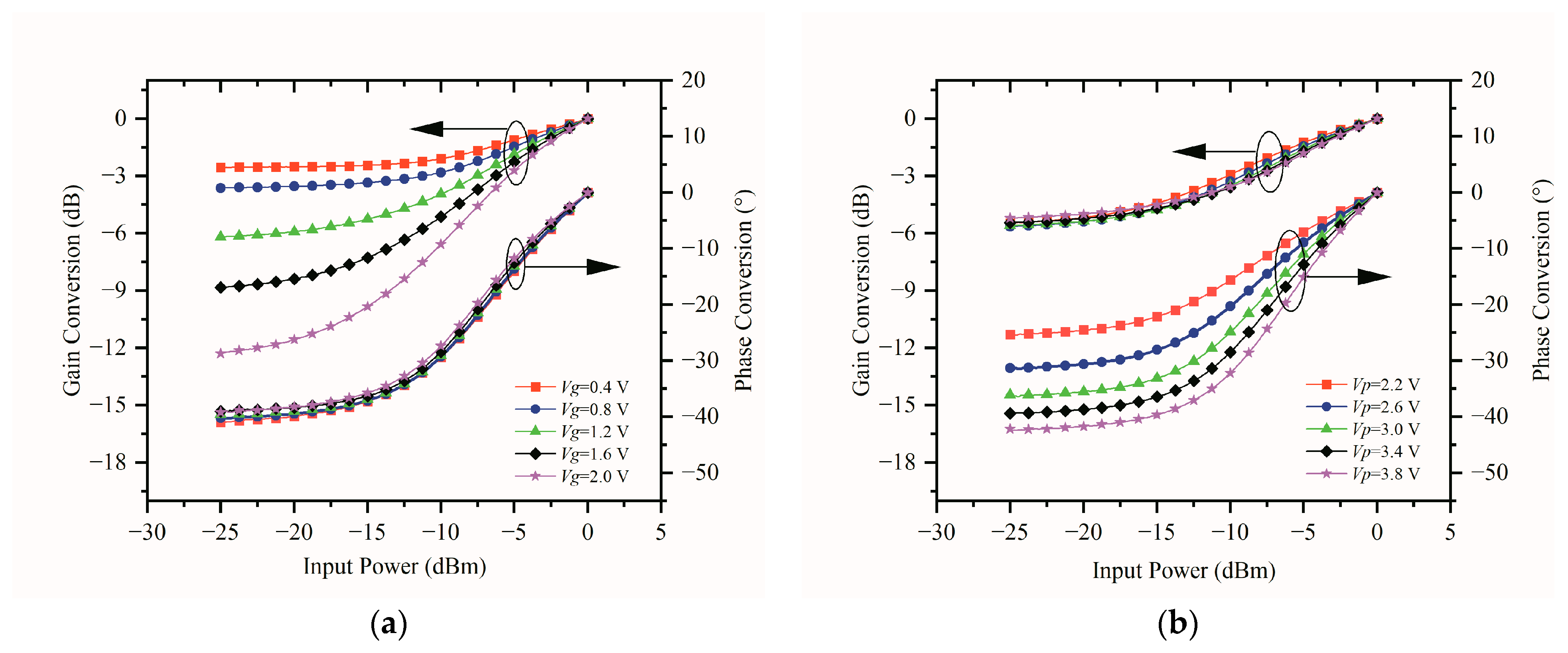
A layout-level simulation of the APD MMIC was carried out based on the 0.15 μm GaAs pHEMT process. The simulation platform integrated all the circuit components needed for the proposed circuit, such as the Schottky diode, capacitor, resistor, etc., and especially the large signal simulation model for the Schottky diode. The Lange coupler and Wilkinson power divider were obtained from the process library. The output amplitude flatness of Lange coupler was less than 0.3 dB, and the return loss and isolation were both less than −25 dB in the bandwidth range of 24~28 GHz. The output amplitude flatness of the Wilkinson power divider was less than 0.3 dB, and the return loss and isolation are both less than −24 dB. A two-finger 20 μm Schottky diode with a bias resistance of 4 kΩ was adopted as nonlinearity generation component of the gain nonlinear branch. When the power supply increased from 0.4 V to 2.0 V, the DC current was less than 1 mA. A four-finger 40 μm Schottky diode with a bias resistance of 1 kΩ was adopted as the nonlinearity generation component of the phase nonlinear branch. When the power supply increased from 2.2 V to 3.8 V, the DC current was less than 3 mA.
The APD MMIC simulation results for the independent tuning of gain and phase conversion are shown in Figure 5. For a clearer comparison, the gain and phase under large signal excitation are normalized to 0 dB and 0°, respectively. When the bias voltage V p of the phase branch remained unchanged at 3.4 V, the bias voltage V g of the gain branch gradually increased from 0.4 V to 2.0 V. The phase expansion remained steady at 47°, while the gain expansion increased from 3.2 dB to 10.5 dB. The gain expansion change was mainly realized through the decrease in the small-signal gain. When the bias voltage V g of gain branch remained unchanged at 1.1 V and the bias voltage V p of the phase branch gradually increased from 2.2 V to 3.8 V, the gain expansion remained unchanged at 4.5 dB, while the phase expansion increased from 28.2° to 50.5°. The phase expansion change was mainly realized through the decrease in the small-signal phase. The gain and phase expansion can be independently adjusted by altering the bias voltages V g and V p of the two nonlinear branches.

3.2. Nonlinear Frequency Adjustment Module Design for Broadband Application

3.2.1. Nonlinear Frequency Adjustment Module Design Principle

The gain compression of a Ka-band TWTA is about 7 dB at the operating band of 25.1~27.5 GHz, and decreases as the frequency is increased, exhibiting a difference for about 1.5 dB in the operating band. The phase compression of a TWTA is about 40° and increases with frequency, having a difference of about 20° in the operating band. It can be seen that the gain compression difference is comparatively smaller than the phase compression difference. To obtain a better nonlinearity of TWTA through cascaded APD MMICs, the phase expansion of the APD MMIC in the operating band should increase more with frequency.
The NFAM is used to realize the desired phase expansion difference. A capacitance in parallel to the gain branch can be used as an NFAM, at the position shown in Figure 1. The gain and phase change in the signal passing through the NFAM can be expressed as G N and φ N , as expressed in Equations (14) and (15), where Z 0 is the characteristic impedance of the microstrip in the gain branch in parallel with C j . G N and φ N are both affected by the capacitance value C j . Through reasonable design, a small gain expansion difference and a large phase expansion difference can be realized in the APD MMIC within the operating band.
G N = 2 4 + ( ω C j Z 0 ) 2
Φ N = arctan ( ω C j Z 0 2 )

3.2.2. Simulation of the NFAM Effect

The influence of the capacitance value on the phase expansion difference is shown in Figure 6a. A capacitance value of 65 fF was used in the APD MMIC. The gain and phase conversion in the operating band are shown in Figure 6b. The gain and phase under small-signal excitation are normalized to 0 dB and 0°, respectively. The gain and phase conversion differences were about 1 dB and 13°, respectively, which is consistent with the corresponding differences of the TWTA in the operating band.

4. Experimental Results

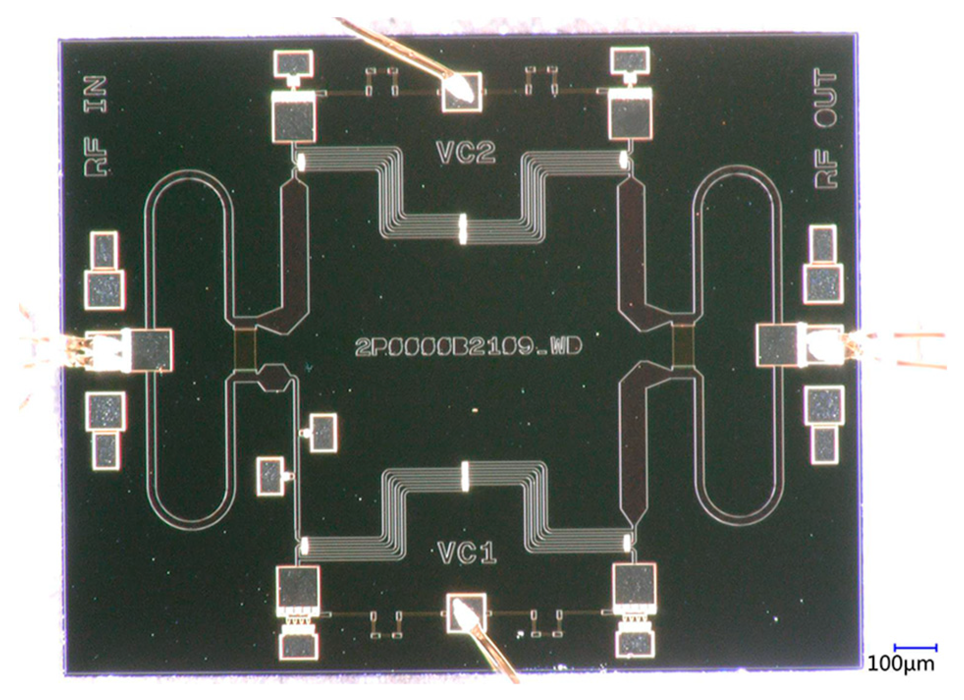
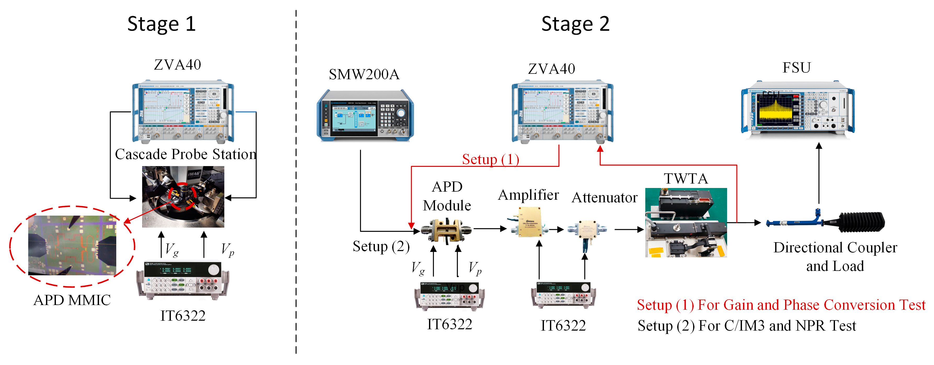
The proposed APD MMIC was implemented using 0.15 μm GaAs pHEMT technology. The size was 1.6 mm × 2.0 mm, and the operating current was less than 10 mA. The chip is shown in Figure 7. The nonlinear performance of the APD MMIC and a TWTA cascaded with the APD MMIC were investigated. The measurement process was divided into two stages. During Stage 1, measurements were carried out on a wafer for the APD MMIC. A vector network analyzer and power supply were connected to the APD MMIC through a Cascade EPS150RF probe station. In Stage 2, the APD MMIC was packaged in a Kovar casing and cascaded with a driver amplifier and an adjustable attenuator to drive a Ka-band 65 W TWTA. The output power at 1 dB gain compression (P1dB) of the driver amplifier was 18 dBm over the frequency range of 25.1~27.5 GHz, which is far greater than the saturated input power of TWTA. The gain flatness of the driver amplifier and the adjustable attenuator was lower than 1.0 dB in the operating band, which ensures that the TWTA can be pushed to the saturated output power state without affecting the nonlinearity and gain flatness of the system when they are connected to the system. In “Setup (1)” of Figure 8, the vector network analyzer ZVA40 was used to perform the gain and phase compression tests of the TWTA and linearized traveling wave tube power amplifier (LTWTA). “Setup (2)” shows the measurement process of the third-order intermodulation signal (C/IM3) and the Noise Power Ratio (NPR). The vector signal source SMW200A was employed to provide a dual-tone signal and a broadband noise signal. The signal analyzer FSU was used to perform the C/IM3 and NPR tests of the TWTA and LTWTA. Before testing, a SOLT and power calibration procedure were carried out to remove the influence of the connecting lines.
To verify the nonlinear characteristics of the APD MMIC, it was necessary to test its gain and phase expansion at the operating band of 25.1~27.5 GHz in Stage 1. The test results are shown in Figure 9. The gain and phase under small-signal excitation are normalized to 0 dB 0°, respectively. When V g = 1.1 V and V p = 3.4 V, a gain and phase expansion of 4.5 dB and 40°, respectively, were realized at the center frequency of 26.3 GHz. The gain expansion of the APD MMIC was 4 dB at the lowest frequency of 25.1 GHz and 5 dB at the highest frequency of 27.5 GHz over the whole operating band, i.e., decreasing as the frequency increased. The phase expansion was 35° at the lowest frequency and 45° at the highest frequency, increasing over the range. The phase expansion difference with frequency was consistent with the phase compression change in the TWTA over the whole operating band and is therefore very suitable for compensating broadband phase expansion characteristics of the TWTA. The gain under saturation and small-signal excitation are shown in Figure 9b, which shows that the chip has good gain flatness over the operating frequency band. By comparing the simulated and measured data of MMIC gain under saturation and a small-signal excitation, it was found that the simulated and measured data are in good agreement with an error of less than 5%.
During the Stage 1 experiments, the independent tuning of gain and phase conversion was also verified at 26.3 GHz. The test results are shown in Figure 10. For a clear comparison, the gain and phase under large signal excitation are normalized to 0 dB and 0°, respectively. As the bias voltage V g of the gain nonlinear gradually increased from 0.4 V to 2.0 V, while the bias voltage V p of the phase branch remained at 3.4 V, the phase expansion remained unchanged at 40° and the gain expansion increased from 2 dB to 13 dB. When the bias voltage V p of the phase branch gradually increased from 2.2 V to 3.8 V with the bias voltage V g of the gain branch steady at 1.1 V, the gain expansion remained unchanged at 5.0 dB while the phase expansion increased from 25° to 40°. In these experiments, the gain (phase) expansion adjustment was realized through a decrease in the small-signal gain (phase) but the saturated gain (phase) change was very small. The measurement results were consistent with the simulation results. It can be seen that the gain and phase expansions can be independently adjusted by adjusting the bias voltages V g and V p .
During Stage 2, the APD MMIC was packaged into a Kovar casing to form a linear module. The nonlinear properties of the TWTA before and after the linear module such as gain compression and phase compression, C/IM3, and NPR were verified. It can be seen from Figure 11 that the gain compression of the TWTA cascaded with the linear module was reduced from 50° to within 12° over the whole operating band, while the gain compression was reduced from 8 dB to less than 3 dB, which means that the linear module compensates the nonlinearity of the TWTA very well.
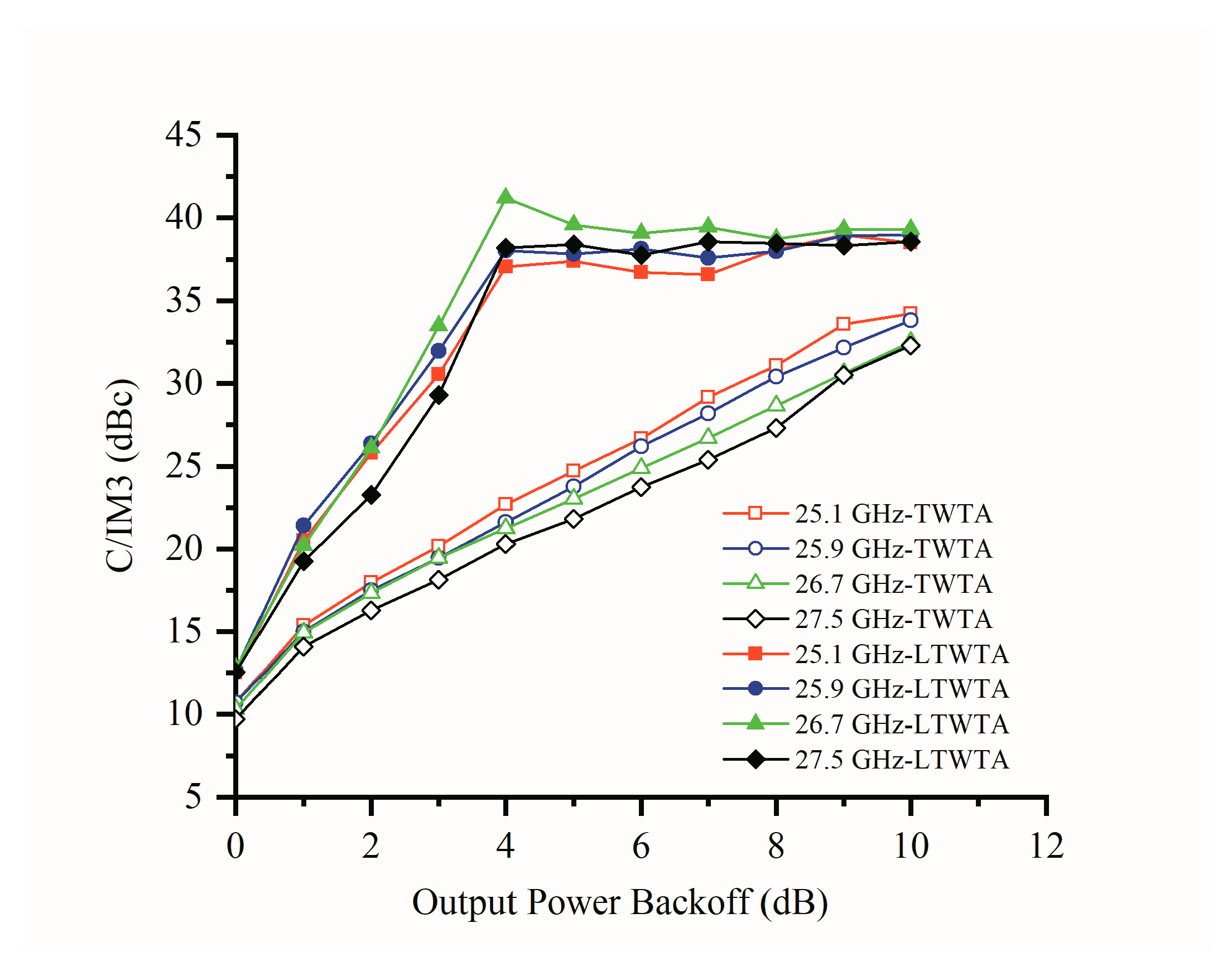
The C/IM3 metric is often used to measure LTWTA nonlinearity under narrowband signal excitation. It is necessary to check the factors that affect C/IM3, such as the power clutter, the bottom noise of the spectrum analyzer FSU, and the P1dB of the drive amplifier before the C/IM3 test. During the test, the amplitude of the spectrometer needs to be set reasonably to ensure that the test data truly reflect the C/IM3 value of the DUT. The frequency interval of the dual-tone signals used in the C/IM3 test was 5 MHz. The measurement results are shown in Figure 12. Due to the adoption of the linear module, the C/IM3 of the LTWTA reached 28 dBc at the 3 dB output power backoff (OPBO) over the whole working band. At 4 dB OPBO, the C/IM3 of the LTWTA was larger than 34 dBc. The output power fallback of the LTWTA under the same C/IM3 value of 28 dBc was 5 dB lower when compared with that of the TWTA. That is to say, the LTWTA can operate at a higher power state and its efficiency is also higher. When the output power fell back 3 dB over the whole operating band 25.1~27.5 GHz, the minimum and maximum C/IM3 values were 28 dBc and 33 dBc. The difference was not more than 5 dB, which indicates that the linear module has good broadband adaptability.
The NPR index is used to measure the nonlinearity of LTWTAs under broadband signal excitation [15]. The noise signal was generated using the NPR software of Rohde & Schwarz, and the noise width can be set from 50 MHz to 500 MHz. The noise gap bandwidth was 5% of the signal bandwidth, and the gap depth was greater than 45 dB. During the NPR test, the four frequency points of 25.4 GHz, 26 GHz, 26.5 GHz, and 27.1 GHz were used as the center frequencies of the noise signals. The noise signal bandwidth ranged from 100 MHz to 500 MHz to observe the impact of the noise bandwidth change on the NPR index when the output power of the LTWTA fell back to 3 dB. The test results are shown in Figure 13. As the noise bandwidth changed, the NPR remained between 15.8 dBc and 17.1 dBc. Since the random signal adopted by the NPR test added an error of ±0.4 dB to the NPR test results [15], it can be considered that the change in the noise signal bandwidth from 100 MHz to 500 MHz had no impact on the NPR index when the output power of LTWTA was reduced to 3 dB, which means that the LTWTA has good broadband characteristics.

5. Discussion

The experimental results show that the APD MMIC with independent adjustment capability for TWTAs can be realized through appropriate diode size selection and adoption of the double-branch vector synthesis circuit structure. The MMIC design can be independent of the TWTA design. For the case of multiple LTWTAs operating simultaneously in a MIMO scenario, because of the wide gain and phase expansion adjustment ranges, one-to-one adaptation can be realized according to the gain and phase characteristics of each TWTA, so the nonlinear indices of LTWTA can be improved effectively. Comparing the C/IM3 of the LTWTA and the TWTA, the output power fallback of the LTWTA under the same C/IM3 value of 28 dBc was 5 dB lower than that of the TWTA, which means that the LTWTA can work at a higher power state and its efficiency will be higher, which is a key energy consumption index for satellite communication systems.
The APD MMIC design adopts the NFMA to realize the broadband TWTA phase compression change with the operating frequency, which grants the APD MMIC phase expansion the same characteristics as the TWTA. The proposed APD MMIC achieves good compensation for the TWTA phase compression in the broadband range and improves the nonlinearity of the broadband signal. From the perspective of the broadband nonlinearity index of NPR, a change in the signal bandwidth from 100 MHz to 500 MHz does not lead to a serious deterioration of the NPR, which to some extent shows the effectiveness of NFAM in improving the broadband characteristics of APD MMIC.
A comparison with some recent analog linearization works for PA is given in Table 2. Considering the linearization performance and operating band, the APD MMIC design is comparable to state of the art. while the APD MMIC is small in size and highly integratable, which is very suitable when combined with other control or temperature compensation functions at the front-end of the power amplifier to form a linear channel amplifier with complex functions.
In future work, the memory effect caused by the influence of broadband complex modulation signals on the diode supply voltage of the APD circuit will be considered, and its influence will be reduced through APD circuit design modifications. Furthermore, the integration of analog APD and digital APD technology will be considered from the aspect of power amplifier linearization, where APD is used to compensate for nonlinearity and DPD to eliminate the memory effect with the aim of proposing a broadband power amplifier linearization solution while reducing the complexity of the DPD algorithm.

6. Conclusions

In this paper, a Ka-band broadband APD MMIC with an area of 1.6 mm × 2.0 mm is proposed based on the 0.15 μm GaAs pHEMT process. The APD circuit has independent gain and phase adjustment capabilities, which is suitable for the nonlinear compensation of multiple TWTAs with inconsistent nonlinearities. The independent tuning performance of gain and phase conversion improves the compensation accuracy effectively. Meanwhile, the APD MMIC achieves broadband phase matching with a TWTA in the operating bandwidth of 25.1~27.5 GHz through the addition of the NFAM. When the APD MMIC is combined with a Ka-band TWTA, the gain compression is reduced from 7 dB to 3 dB and the phase compression is reduced from 40° to 12°. When OPBO = 3 dB, the C/IM3 is better than 28 dBc over the whole operating band and the NPR remains basically steady and better than 15.7 dBc as the signal bandwidth increases from 100 MHz to 500 MHz, which shows that the APD circuit can improve the nonlinearity of broadband TWTAs effectively. This type of APD circuit has high consistency in batch production. Moreover, due to its small size and monolithic design, it is very suitable for integration with other microwave circuits in the front-end of TWTAs to form an APD microwave module with complex and diverse functions.

Author Contributions

Conceptualization, T.L., X.S. and G.W.; methodology, T.L., X.S. and G.W.; software, T.L. and R.F.; validation, T.L., R.F. and D.Z.; formal analysis, T.L.; investigation, T.L. and B.Z.; resources, T.L. and D.Z.; data curation, T.L.; writing—original draft preparation, T.L.; writing—review and editing, B.Z., X.S. and G.W.; visualization, T.L.; supervision, T.L.; project administration, T.L.; funding acquisition, T.L. All authors have read and agreed to the published version of the manuscript.

Funding

This research received no external funding.

Data Availability Statement

Not applicable.

Conflicts of Interest

The authors declare no conflict of interest.

References

  1. Katz, A.; Gray, R.; Dorval, R. Linearizers for Q- and V-Band TWTAs. IEEE Trans. Electron Devices 2018, 65, 2317–2377. [Google Scholar] [CrossRef]
  2. Gupta, A.; Jha, E.R.K. A survey of 5G network: Architecture and emerging technologies. IEEE Access 2015, 3, 1206–1232. [Google Scholar] [CrossRef]
  3. Guan, L.; Zhu, A. Green communications: Digital predistortion for wideband RF power amplifiers. IEEE Microw. Mag. 2014, 15, 84–99. [Google Scholar] [CrossRef] [Green Version]
  4. Xi, T.; Huang, S.; Guo, S.; Gui, P.; Huang, D.; Chak, S. High-efficiency E-band power amplifiers and transmitter using gate capacitance linearization in a 65-nm CMOS process. IEEE Trans. Circuits Syst. II Exp. Briefs 2017, 64, 234–238. [Google Scholar] [CrossRef]
  5. Shi, B.; Leong, S.W.; Zhai, G.; Wang, W.; Luo, B. Development of Ka-band BUC with wideband linearizer for high speed satellite communications. In Proceedings of the IEEE Global Communications Conference (GLOBECOM), Singapore, 4–8 December 2017; pp. 1–6. [Google Scholar]
  6. Cai, Q.; Che, W.Q.; Ma, K.X.; Zhang, M. A simplified transistor based analog predistorter for a GaN power amplifier. IEEE Trans. Circuits Syst. II Exp. Briefs 2018, 5, 326–330. [Google Scholar] [CrossRef]
  7. Zhang, H.; Sánchez-Sinencio, E. Linearization techniques for CMOS low noise amplifiers: A tutorial. IEEE Trans. Circuits Syst. I 2011, 58, 22–36. [Google Scholar] [CrossRef]
  8. Shen, Y.; Hraimel, B.; Zhang, X.; Cowan, G.; Wu, K.; Liu, T. A novel analog broadband RF predistortion circuit to linearize electro-absorption modulators in multiband OFDM radio-over-fiber systems. IEEE Trans. Microw. Theory Tech. 2010, 58, 3327–3335. [Google Scholar] [CrossRef]
  9. Katz, A.; Wood, J.; Chokola, D. The Evolution of PA Linearization. IEEE Microw. Mag. 2016, 17, 32–40. [Google Scholar] [CrossRef]
  10. Li, C.; He, S.; You, F.; Peng, J.; Hao, P. Analog Predistorter Averaged Digital Predistortion for Power Amplifiers in Hybrid Beam-Forming Multi-Input Multi-Output Transmitter. IEEE Access 2020, 8, 146145–146153. [Google Scholar] [CrossRef]
  11. Park, C.-W.; Beauregard, F.; Carangelo, G.; Ghannouchi, F.M. An independently controllable AM/AM and AM/PM predistortion linearizer for CDMA 2000 multicarrier applications. In Proceedings of the IEEE Radio Wireless Conference, Phoenix, AZ, USA, 19–22 August 2001; pp. 53–56. [Google Scholar]
  12. Deng, H.; Zhang, D.; Lv, D.; Zhou, D.; Zhang, Y. Analog Predistortion Linearizer with Independently Tunable Gain and Phase Conversions for Ka-Band TWTA. IEEE Trans. Electron Devices 2019, 66, 1533–1539. [Google Scholar] [CrossRef]
  13. Deng, H.; Lv, D.; Zhang, Y.; Zhang, D.; Zhou, D. Compact Analog Predistorter with Shape Tuning Capability Using Power-Dependent Impedance Matching Network. IEEE Trans. Circuits Syst. II Express Briefs 2020, 67, 1705–1709. [Google Scholar] [CrossRef]
  14. Zhang, W.-M.; Yuen, C. A Broadband Linearizer for Ka-Band Satellite Communication. In Proceedings of the 51st ARFTG Conference Digest, Baltimore, MD, USA, 12 June 1998; pp. 1203–1206. [Google Scholar]
  15. Villemazet, J.-F.; Yahi, H.; Lefebvre, B.; Baudeigne, F.; Maynard, J.; Soubercaze-Pun, G.; Lapierre, L. New Ka-Band Analog Predistortion Linearizer allowing a 2.9 GHz Instantaneous Wideband Satellite Operation. In Proceedings of the 47th European Microwave Conference, Nuremberg, Germany, 8–10 October 2017; pp. 1042–1045. [Google Scholar]
  16. Hao, P.; He, S.; You, F.; Li, C. Independently Tunable Linearizer Based on Characteristic Self-Compensation of Amplitude and Phase. IEEE Access 2019, 7, 131188–131200. [Google Scholar] [CrossRef]
  17. Iommi, R.; Macchiarella, G.; Meazza, A.; Pagan, M. Study of an Active Predistorter Suitable for MMIC Implementation. IEEE Trans. Microw. Theory Techn. 2005, 53, 874–880. [Google Scholar] [CrossRef]
  18. Gavell, M.; Granström, G.; Fager, C.; Sten, E.; Zirath, H. An E-Band Analog Predistorter and Power Amplifier MMIC Chipset. IEEE Microw. Wirel. Compon. Lett. 2018, 28, 31–33. [Google Scholar] [CrossRef]
  19. Tsai, J.-H.; Chang, H.-Y.; Wu, P.-S.; Lee, Y.-L.; Wang, H. Design and Analysis of a 44-GHz MMIC Low-Loss Built-In Linearizer for High-Linearity Medium Power Amplifiers. IEEE Trans. Microw. Theory Techn. 2006, 54, 2487–2496. [Google Scholar] [CrossRef]
  20. Yamauchi, K.; Nakayama, M.; Ikeda, Y.; Araki, T. An 18GHz Band MMIC Linearizer Using Parallel Diode with a Bias Feed Resistance and a Parallel Capacitor. In Proceedings of the 2000 IEEE MTT-S International Microwave Symposium Digest, Boston, MA, USA, 11–16 June 2000; pp. 1507–1510. [Google Scholar]
  21. Potschka, J.; Dietz, M.; Kolb, K.; Maiwald, T.; Weigel, R. A Highly Linear and Efficient 28 GHz Stacked Power Amplifier for 5G using Analog Predistortion in a 130 nm BiCMOS Process. In Proceedings of the IEEE Asia-Pacific Microwave Conference (APMC), Singapore, 10–13 December 2019; pp. 920–922. [Google Scholar]
  22. Nguyen, D.P.; Nguyen, N.L.K.; Stameroff, A.N.; Camarchia, V.; Pham, A.-V. A Wideband Highly Linear Distributed Amplifier Using Intermodulation Cancellation Technique for Stacked-HBT Cell. IEEE Trans. Microw. Theory Techn. 2020, 68, 2984–2997. [Google Scholar] [CrossRef]
  23. Zhao, J.; Cooman, A.; Shamsafar, A.; Rousstia, M.; Calzona, D.; Pires, S. A High-Linear Ka-Band Power Amplifier with Diode-Based Analogue Predistortion. In Proceedings of the 15th European Microwave Integrated Circuits Conference, Utrecht, The Netherlands, 10–15 January 2021; pp. 157–160. [Google Scholar]
  24. Xie, X.; Xu, Y.; Xia, L. Microwave Integrated Circuit, 1st ed.; Electronics Industry Press: Beijing, China, 2018; pp. 241–243. [Google Scholar]
  25. Haris, N.; Kyabaggu, P.B.K.; Alim, M.A.; Zhang, Y.; Rezazadeh, A.A. Device Considerations and Characterisations of Double-Channel GaAs pHEMT Schottky Diodes for Limiter Applications. In Proceedings of the 10th European Microwave Integrated Circuits Conference, Paris, France, 7–8 September 2015; pp. 219–222. [Google Scholar]
  26. Huang, H.; Huang, J.; Shi, Q. A parameter extraction method of the Schottky diode millimeter wave equivalent circuit model. J. Infrared Millim. Waves 2021, 40, 32–737. [Google Scholar]
  27. Yamauchi, K.; Mori, K.; Nakayama, M.; Mitsui, Y.; Takagi, T. A microwave miniaturized linearizer using a parallel diode with a bias feed resistance. IEEE Trans. Microw. Theory Techn. 1997, 45, 2431–2435. [Google Scholar] [CrossRef]
  28. Jeong, H.-Y.; Park, S.-K.; Ryu, N.-S.; Jeong, Y.-C.; Yom, I.-B.; Kim, Y. A Design of K-band Predistortion Linearizer using Reflective Schottky Diode for Satellite TWTAs. In Proceedings of the 13th GAAS Symposium, Paris, France, 4–6 October 2005; pp. 597–600. [Google Scholar]
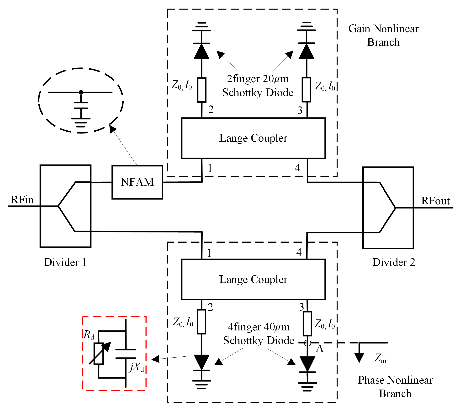
Figure 1. Analog predistortion MMIC schematic.
Electronics 12 01503 g001
Figure 2. (a) The GaAs pHEMT diode layout; (b) the GaAs pHEMT diode model.
Electronics 12 01503 g002
Figure 3. I-V curve for different sizes of GaAs pHEMT Schottky diodes.
Electronics 12 01503 g003
Figure 4. Schematic diagram of (a) gain expansion and (b) phase expansion independently tuning.
Electronics 12 01503 g004
Figure 5. Simulated results of the independent tuning of (a) gain conversion and (b) phase conversion.
Electronics 12 01503 g005
Figure 6. (a) Phase expansion difference with Cj. (b) Gain and phase expansion after adding NFAM to APD MMIC.
Electronics 12 01503 g006
Figure 7. APD MMIC Photo.
Electronics 12 01503 g007
Figure 8. The test platform for APD MMIC and TWTA cascade with proposed APD MMIC.
Electronics 12 01503 g008
Figure 9. Measured results of (a) gain and phase expansion and (b) gain under saturation and small signal.
Electronics 12 01503 g009
Figure 10. Measured results of independent tuning of (a) gain conversion and (b) phase conversion.
Electronics 12 01503 g010
Figure 11. TWTA gain and phase conversion before and after the proposed APD MMIC circuit.
Electronics 12 01503 g011
Figure 12. The C/IM3 performance before and after the proposed APD MMIC circuit.
Electronics 12 01503 g012
Figure 13. NPR performance of LTWTA with a signal width change when OBO = 3 dB.
Electronics 12 01503 g013
Table 1. DC parameter of diodes with different sizes.
Diode Size I s (pA) R s (Ω)n
One-finger 10 μm7.910.151.37
Two-finger 20 μm28.920.111.37
Four-finger 40 μm93.910.091.37
Table 2. Comparison with similar APD linearizers.
ReferenceOperating
Band
Signal
Bandwidth
C/IM3 or ACPR
Improvement
Independently TunableCo-Design with PASizeTechnique
[12] 29~31 GHzN/A9@3 dB
OPBO(C/IM3)
YesNo28.5 × 31.4 mm2HMIC 2
[13]5.5~5.8 GHzN/A13@3 dB
OPBO(C/IM3)
YesNoN/AHMIC
[16] 3.4~3.6 GHz55 MHz8.4@6 dB
OPBO(ACPR 1)
YesNoN/AHMIC
[19] 40~50 GHz1 MHz8@3 dB
OPBO(ACPR)
NoYes2.0 × 1.0 mm2MMIC
[22] DC~90 GHzN/A9@3 dB
OPBO(C/IM3)
NoYes1.6 × 0.7 mm2MMIC
This work25.1~27.5 GHz500 MHz10@3 dB
OPBO(C/IM3)
YesNo2.0 × 1.6 mm2MMIC
1 ACPR refers to the adjacent channel power ratio. 2 HMIC refers to the hybrid microwave integrated circuit.
Disclaimer/Publisher’s Note: The statements, opinions and data contained in all publications are solely those of the individual author(s) and contributor(s) and not of MDPI and/or the editor(s). MDPI and/or the editor(s) disclaim responsibility for any injury to people or property resulting from any ideas, methods, instructions or products referred to in the content.