Abstract
Microwave imaging is a high-resolution, noninvasive, and noncontact method for detecting hidden defects, cracks, and objects with applications for testing nonmetallic components such as printed circuit boards, biomedical diagnosis, aerospace components inspection, etc. In this paper, an array of microwave sensors designed based on complementary split ring resonators (CSRR) are used to evaluate the hidden features in dielectric media with applications in nondestructive testing and biomedical diagnosis. In this array, each element resonates at a different frequency in the range of 1 GHz to 10 GHz. Even though the operating frequencies are not that high, the acquisition of evanescent waves in extreme proximity to the imaged object and processing them using near-field holographic imaging allows for obtaining high-resolution images. The performance of the proposed method is demonstrated through simulation and experimental results.
1. Introduction
Nonmetallic and dielectric components are highly in demand throughout various industries due to advantages such as low-cost, light weight, resistance to corrosion, durability, and more. Material technology has produced lighter, stiffer, stronger, and more durable electrically insulating composites which are replacing metallic components in various applications [1]. For instance, the use of certain types of composites allows commercial airplanes to operate with higher pressure and humidity [2] while being lightweight. Furthermore, these components are often assumed to be in perfect condition for printed circuit board (PCB) testing, aerospace components, and more, though there may be cracks, defects, or even objects present that are undesirable due to abruptions, unforeseen changes, delamination, and unpredictable processing of these materials. Therefore, it is critical to detect these features to prevent unexpected consequences.
To resolve this problem, microwave imaging and sensing for nonmetallic and dielectric components have been popular among all nondestructive testing (NDT) techniques due to their promising results [3]. Microwave NDT features advantages such as being noncontact, low power, compact, robust, and able to obtain images with high resolutions [1]. Therefore, microwave NDT has been applied to different applications. For example, the electronic industry is concerned with delamination in composite materials that are used for PCB substrates. This leads to strength deterioration and results in structural failure. To address this problem, an electromagnetic band gap (EBG) planar microwave microstrip sensor has been proposed in [4] to detect delamination in fiber-reinforced epoxy-based PCB laminates. Similarly, an automatic crack detection technique for the quality check of FR4 has been proposed in [5] where a microwave planar sensing probe has been designed. Furthermore, in [1], the capability of near-field microwave NDT methods for detecting and evaluating corrosion under paint has been shown. Another application of high-resolution imaging of dielectric media is in estimating the size of tumors in early-stage malignant melanoma skin cancer [6,7].
Various configurations of microwave sensors have been utilized depending on the targeted applications. For example, in [8], a spiral resonator excited by an electrically small loop is employed for microwave near-field imaging of various defects. Furthermore, a split-ring resonator sensor has been designed for near-field microwave imaging of composites through edge coupling [9]. Noninvasive measurements of thickness and permittivity in multilayered dielectric structures using complementary split ring resonator (CSRR) sensors have been proposed in [10]. Furthermore, different types of CSRR sensors have also been designed and used for microwave imaging of subsurface flaws in coated metallic structures [11] and composite structures [12].
In the previous works, typically, the raw responses obtained from the microwave sensors are plotted versus spatial parameters to obtain images of the defects. They lack more advanced postprocessing that could lead to a higher quality assessment of the material. High-resolution imaging results have been presented in [13,14,15] where near-field holographic imaging has been proposed and applied to the data collected at the near-field of the antennas. The advantages of near-field holographic imaging are: (1) far-field assumptions in conventional holographic imaging are avoided by introducing a new formulation of the solution for the imaging problem, (2) it is capable of processing the evanescent waves leading to higher resolutions beyond the diffraction limit, (3) the assumption for point-wise antennas typically used in conventional holographic imaging is avoided due to the measurement of the so-called point-spread function (PSF), and (4) unlike conventional holographic imaging, it is possible to use the measurement for an array of receiver antennas and achieve super-resolution using narrowband data. In [13], wide-band near-field holographic imaging has been implemented for the inspection of nonmetallic pipes. In [14], imaging results for nonmetallic concentric pipes based on microwave holographic imaging and a standardized minimum norm approach have shown improvement compared to the minimum norm approach. There, narrowband data collected by an array of receiver antennas have been employed for the inspection of double concentric pipes. A similar setup has been also used in [15] for thickness profile estimation of a single nonmetallic pipe.
Other than microwave imaging technology, recent works of imaging using near-field-scanning optical microscope technology [16,17] have demonstrated high-resolution results at the nanometer level. However, these imaging techniques can only be applied to surface imaging while the proposed near-field microwave imaging technique can provide images at multiple depths (volumetric imaging). This is achieved by using the capabilities of electromagnetic waves at microwave frequencies to penetrate dielectric media as well as processing the scattered waves with the proposed near-field holographic imaging technique.
In this paper, we propose the utilization of an array of sensors resonating at multiple frequencies ranging from 1 GHz to 10 GHz for assessing the shape features in the dielectric media. For the first time, the responses obtained from a near-field microwave sensor array (we employ the sensor array in [18]) are postprocessed through a robust near-field holographic imaging method. This is in contrast to the previous works which normally plot the raw data measured by the near-field microwave sensors to produce images. We have used the rectangular CSRR structure due to the simple design process. Please note that the main idea of this work is that, in contrast to other CSRR sensors mentioned above, the utilized sensor in this work is multifrequency, whereas other CSRR sensors are single elements and provide responses at only one frequency. In other words, more information is provided by using the proposed sensor allowing for volumetric imaging when employing near-field holographic imaging. Simulation and experimental results demonstrate the performance of the proposed system in achieving high resolution in imaging dielectric media with applications in NDT and biomedical diagnosis.
2. Theory
In this section, we present the theory of near-field holographic imaging for a multifrequency near-field sensor. The data acquisition and image reconstruction are performed over flat surfaces (along the x and y axes) at various z. In addition, the scattered field is recorded by the same sensor at each position . Then, the complex-valued scattered field, , is measured at each sampling position, at frequencies within the band of to , by the sensor. Each frequency component is measured by a particular element in the sensor array.
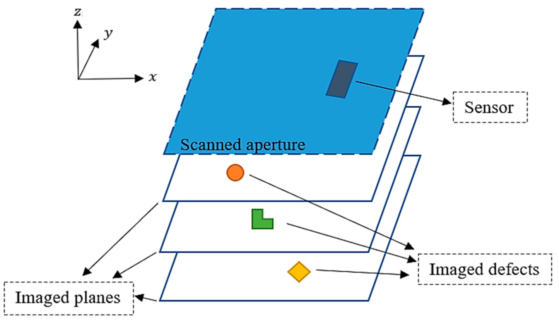
Figure 1 illustrates the proposed microwave holographic imaging setup that consists of a multifrequency near-field sensor that collects back-scattered data over a rectangular aperture. Such a scattered response is acquired by subtracting the response without the presence of the objects from the response with the objects. The image reconstruction process then provides images over the planes, where . The distance between the planes is denoted by . The imaging system is assumed to be linear (using Born approximation [19]) and space invariant (LSI).
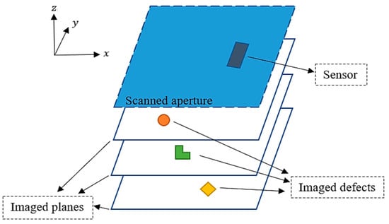
Figure 1.
Illustration of the near-field microwave holographic imaging setup.
Holographic imaging will be implemented as follows. First, the point-spread functions (PSFs) of the LSI imaging system are obtained. These PSFs are denoted by and are approximated by measuring small objects called point-wise objects (POs) placed on each imaged plane (at ) one at a time. The scattered response recorded for a PO placed on the i-th depth is denoted by . Then, according to the convolution theory, the object’s response for each imaged plane, , can be written as the convolution of the collected PSF for that plane, , with the contrast function of the object on the corresponding plane . Next, the response due to the objects on the material under test (MUT), , can be obtained from the superposition of the responses of all of the imaged planes, , where , as:
Here, and denote convolution along x and y, respectively. In Equation (1), PSF functions can be obtained a priori through simulation or measurement. In addition, is derived by recording the responses for the objects on MUT. The goal is then to estimate the contrast functions of the objects , where it relates to the wavenumbers of the object, , and background medium, , as [20].
Furthermore, measurements can be implemented at multiple frequencies, , , to provide more data for image reconstruction. Thus, Equation (1) can be written at all frequencies and after applying discrete-time Fourier transform (DTFT) along the x and y directions, we obtain the following system of equations at each spatial frequency pair and are the Fourier variables corresponding to x and y variables):
where, , , and are DTFTs of , , and , respectively. Then, Equation (3) can be written as:
where
After solving these systems of equations at each , we obtain , . In [14], it has been shown that using a standardized minimum norm alleviates the depth biasing problem, i.e., the underestimation of deep features in favor of more superficial ones. Thus, here, we also employ this approach to solve the system of equations in Equation (4). The solution can be obtained as:
where
Here, is the identity matrix, is a vector of ones, is Hermitian transpose operation, denotes Moore–Penrose pseudoinverse, and is the diagonal matrix formed by the diagonal elements of .
After obtaining values, inverse DTFT along x and y directions are applied to reconstruct images, , at , . At last, the normalized images, ||/M, where M is the maximum of || for all , are plotted.
Noted, diffraction-limited resolution can be overcome here due to the measurement of parts of the evanescent waves spectrum in the near-field systems. This is because in far-field diffraction-limited systems, the wavenumber is within the range of [−2,2] while in our near-field measurement system values beyond this range can be measured and processed leading to higher resolutions.
Moreover, in cases we are interested in evaluating the overall thickness of a long object along the z axis, the normalized images can be combined to obtain the total thickness of the object. This is implemented as:
As discussed later, this has applications in defect depth assessment or tumor size estimation.
3. Simulation Results
In this section, the simulation studies for the proposed imaging technique are performed and demonstrated using FEKO software [21]. We utilize a multifrequency near-field sensor, first introduced in [18]. Shown in Figure 2, it is composed of five nonuniform CSRRs with the elements resonating at five frequencies at 1.234 GHz, 3.074 GHz, 4.949 GHz, 6.699 GHz, and 8.3768 GHz. As noted, these resonating frequencies are defined with the presence of an object. The substrate for the sensor is Rogers RO4350 and it has a width of 20 mm, length of of 56 mm, and microstrip line width of 1.68 mm. For other dimensions, please refer to [18]. The sensor has been fabricated by a commercial company using standard PCB fabrication technology. In the following, the simulation study is divided into two applications: defect size estimation in dielectric media and skin tumor size estimation.

Figure 2.
Microwave sensor array with (a) front surface and (b) back surface.
3.1. Assessment of Defects in Dielectric Materials
Figure 3 illustrates the reference setup in which there is a dielectric slab with a thickness of 1 mm above the sensor with a length of L = 200 mm, a width of W = 20 mm, and a height of H = 6 mm. The slab has a relative permittivity of = 4 and a tangent loss of 0.0001. Please note that, here, as a proof of concept, we present the results for one-dimensional (1D) imaging. We scan the sensor over the x axis (z = 0). We aim at evaluating the thickness variation of the slab with a 2 mm resolution while it has hidden defects (on the other side of the slab compared to the sensor position). For this purpose, the thickness of the 6 mm-thick slab can be estimated at three levels: , , and .

Figure 3.
Simulation setup in FEKO for the assessment of defects in dielectric materials.
The 1D scanning of the sensor array is performed along the x direction from −40 mm to 40 mm with 81 steps. Furthermore, for a realistic study, additive white Gaussian noise with a signal-to-noise ratio (SNR) of 20 dB was added to the simulated responses in MATLAB. To determine the thickness and location of the defects, first, small defects representing POs with an opening width (along x axis) and depth (along z axis) of extending over the whole width (along y axis) of the slab are placed at , , and , one at a time to collect the PSF responses.
With reference to Figure 3, three defects with an opening width of 2 mm and depth of , are placed at positions of (x = ±7 mm). As observed in the figure, the defects are on the opposite side of the slab compared to the sensor, representing hidden flaws.
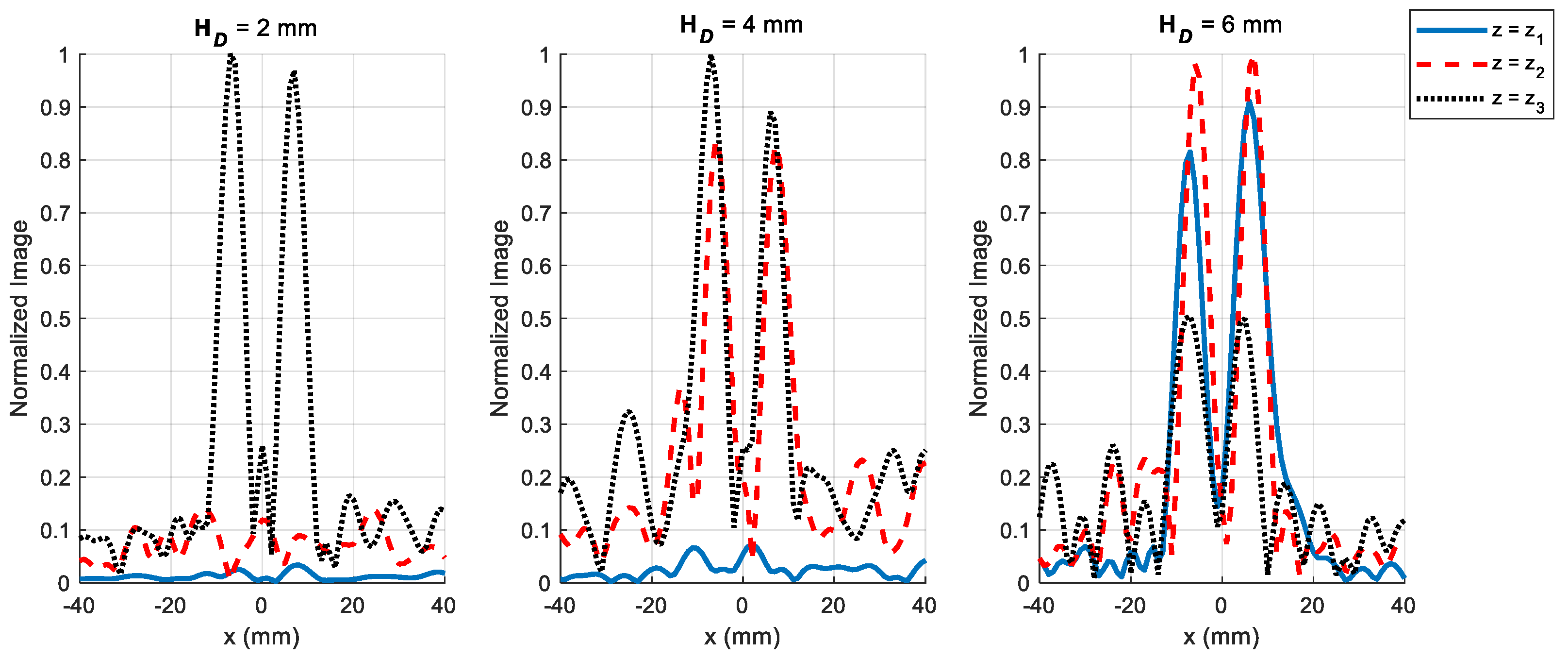
Figure 4 shows the reconstructed 1D images of the defects at the three imaged lines corresponding to the depth positions of the collected PSF responses. It is observed that as the depth of the defect () increases, at some imaged depths the normalized value of the image deviates from 1. This can be explained according to the further violation of the Born approximation for larger defects.
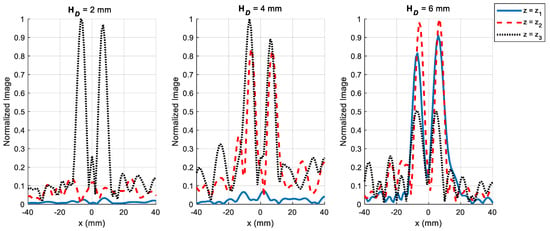
Figure 4.
Reconstructed 1D images for defects with = 2 mm, = 2 mm, = 4 mm, and = 6 mm.
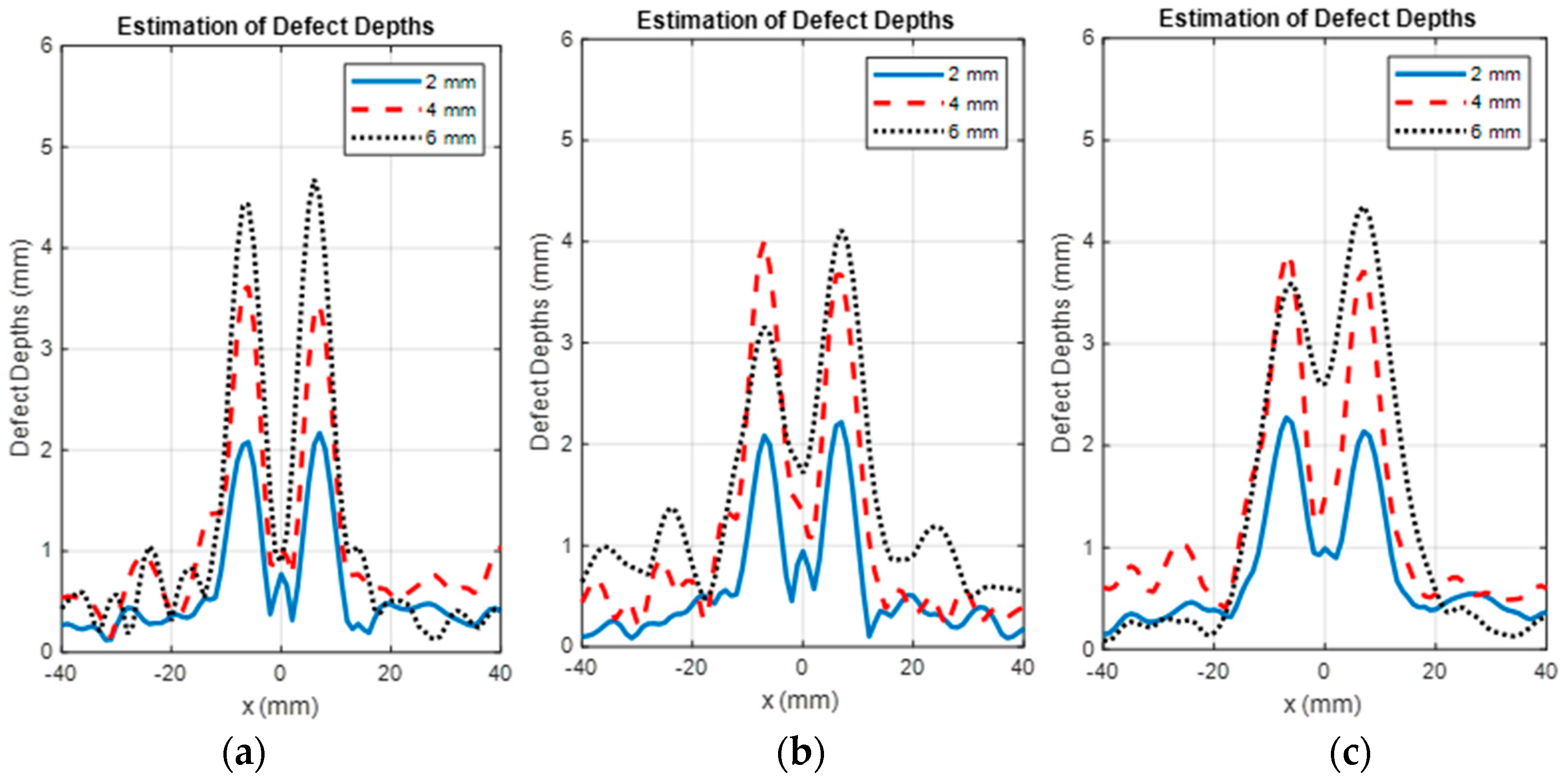
Furthermore, to obtain the estimation of defect thicknesses, the normalized images can be combined as per Equation (12). Figure 5 shows the estimation of the defects’ thicknesses with various . Figure 5a shows the estimation of the defects’ thicknesses with = 2 mm. The best estimation is for the defect with = 2 mm, while the other two larger defects are underestimated compared to their actual depth of 4 mm and 6 mm. In addition, we study the effect of varying the defect opening by decreasing that to 1 mm and increasing that to 3 mm, while the other parameters remain the same as in Figure 5a. Here, Figure 5b,c shows the estimation of defects with = 2 mm, 4 mm, and 6 mm with = 1 mm and 3 mm, respectively. From the two additional studies, it is observed that while for = 2 mm and 4 mm, results are comparable in quality to Figure 5a, for = 6 mm, the depth of defects is significantly underestimated and the capability to resolve the defects is degraded. Overall, the accuracy of the defect depth estimation degrades for larger defects due to the violation of the Born approximation used to derive the proposed estimation technique. To improve the results for larger defects, other microwave techniques based on optimization algorithms have to be employed which are demanding in terms of time and memory compared to the technique proposed here.
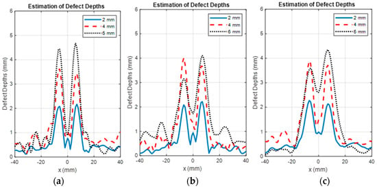
Figure 5.
Thickness estimation of defects with of 2 mm, 4 mm, and 6 mm with (a) = 2 mm, (b) = 1 mm, and (c) = 3 mm.
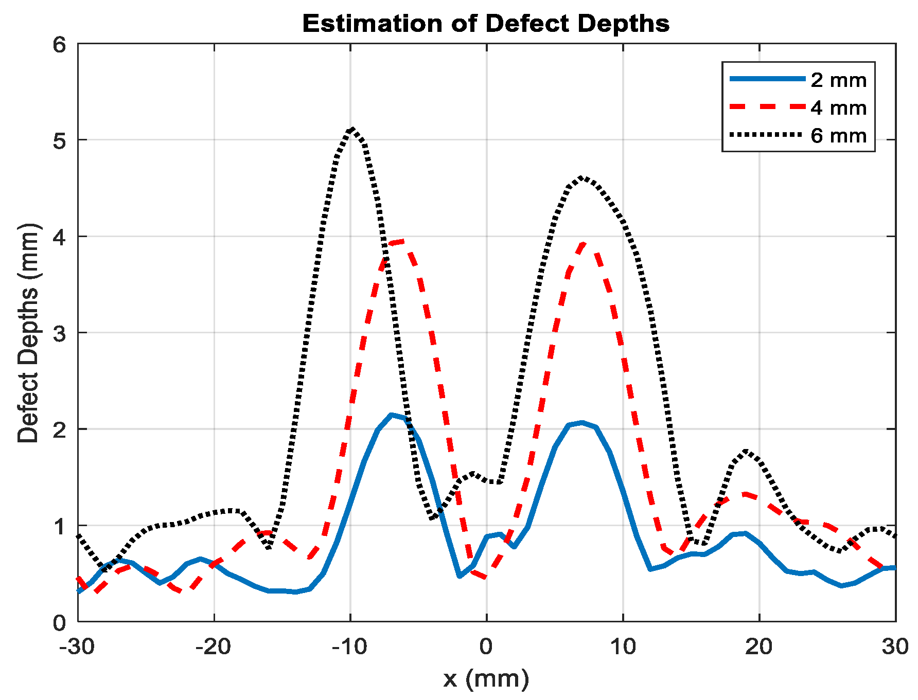
Moreover, we also studied how the coupling effect between the resonators can affect the results by decreasing the edge-to-edge distance between the sensors by one hal which caused the overall length of the sensor array to be smaller. With a shorter array, the 1D scanning is performed along the x direction from −30 to 30 mm with 61 steps. For the dielectric slab, all parameters except the length are kept the same compared to the first example. Figure 6 shows the thickness estimation of defects with of 2 mm, 4 mm, and 6 mm with = 2 mm while utilizing the shorter array. Compared to Figure 5a, it is observed that in Figure 6, there are larger errors in the nondefected regions for of 2 mm, 4 mm, and 6 mm. Furthermore, for of 6 mm, the cross-range resolution is significantly degraded compared to Figure 5a. In other words, coupling between sensors increases which, in turn, leads to larger errors when the resonators get closer. On the other hand, increasing the distance between the resonators increases the length of the sensor array.
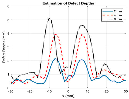
Figure 6.
Thickness estimation of defects with of 2 mm, 4 mm, and 6 mm with = 2 mm with a smaller sensor.
3.2. Skin Tumor Size Estimation
Here, we conduct a simulation study for sizing skin tumors. The human tissue is modeled with human skin and human fat. We use the corresponding dispersive (frequency-dependent) tissue models from the FEKO media library. Furthermore, the relative permittivity and conductivity of the tumor are assumed to be = 50 and 3 S/m, respectively. The relative permittivity of the skin tumor has been reported to be between 35 to 50 in the frequency range of 1 GHz to 10 GHz [22,23]. Here, it is assumed that the sensor scans the tissue in close proximity. The gap between the sensor and skin layer is considered to be 0.1 mm, representing the existence of a thin protective cover. Figure 7 illustrates the simulation setup for skin tumor evaluation when the tumor is on the surface of the skin. Here, the length and width of the skin layer are L = 100 mm and W = 10 mm, respectively. The human fat layer has a thickness of 3 mm and the human skin layer has a thickness of 2 mm. Like the dielectric material simulation setup, 1D scanning of the array of the sensor is implemented along the x direction from −40 to 40 with 81 steps to obtain the responses. In addition, similar to the previous example, noise with an SNR of 20 dB is added to the simulated responses in MATLAB for a practical study. In this example, we consider imaged lines at depths (layers) of 1.5 mm, 3 mm, and 4.5 mm, and PSF data is obtained a priori as in the previous example. We also perform a simulation of the tissues without any tumor to obtain the background responses. These background responses are then subtracted from the responses simulated with the presence of the tumors to obtain the scattered responses.

Figure 7.
Illustration of the simulation setup for skin tumor evaluation in FEKO.
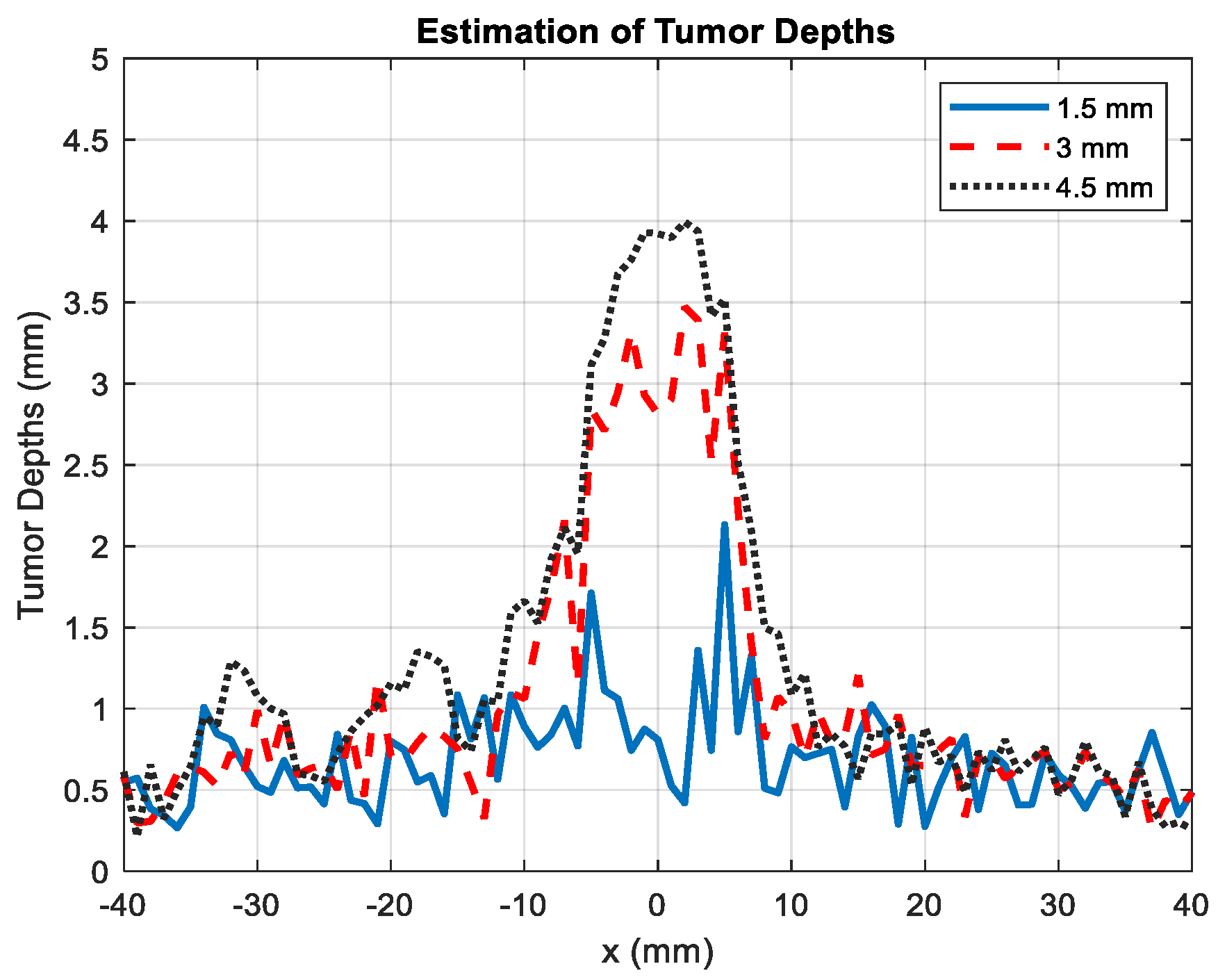
Figure 8 illustrates the simulation setup for skin tumor evaluation with three tumor sizes when the tumor has ingrown deeper. Figure 8a illustrates a smaller tumor with dimensions of and on the surface of the skin. Figure 8b illustrates a larger tumor compared to the one in Figure 8a which has ingrown larger to the middle layer with the dimensions of that on the middle layer as and . Figure 8c illustrates the biggest considered tumor which has ingrown to the farthest layer with the dimensions on the third layer denoted by and . The proposed method is applied to the scattered responses. The estimations of the tumors with depths of 1.5 mm, 3 mm, and 4.5 mm are presented in Figure 9. It is observed that the estimated thicknesses of 1.5 mm and 3 mm are overestimated while for 4.5 mm, it is underestimated by nearly 0.5 mm. The error for estimation of 1.5 mm tumor can be due to the weak signal for such small tumor size while the error for the 4.5 mm tumor is due to the further violation of the Born approximation for larger objects.

Figure 8.
Illustration of the simulation setup for skin tumor evaluation in FEKO with: (a) and , (b) , , , and , and (c) , and .
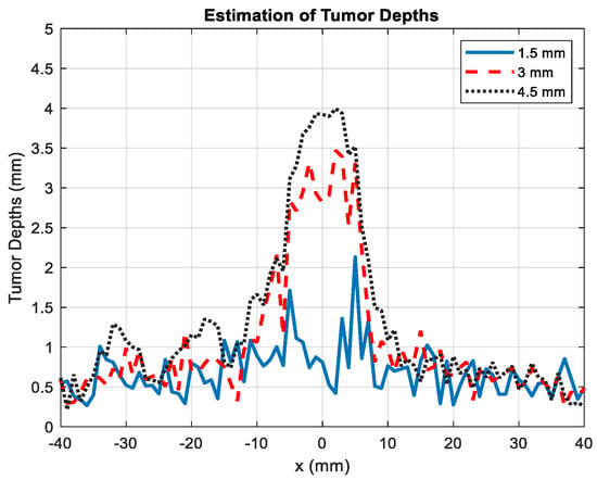
Figure 9.
Depth estimation of the tumor for actual thicknesses of 1.5 mm, 3 mm, and 4.5 mm.
4. Experimental Results
In this section, we present the proof-of-concept experimental results to detect defects and objects using the proposed technique. Figure 10a,b show the microwave imaging system that consists of a scanning system, one Arduino Uno, NEMA 17 stepper motors, MUT, and the sensor. The two types of MUTs used are wood and a pile of paper with 2 mm copper strips hidden inside. For both scenarios, there is an approximate gap of 2 mm between the MUT surface and the sensor. Furthermore, the MUTs are stationary while the sensor is scanning along the x-axis. Then, to reduce the interference, the sensor is backed by a box covered by a microwave-absorbing sheet. Then Figure 10c,d show the front and back of the multifrequency near-field sensor. As noted, an Anritsu MS46122B vector network analyzer (VNA) and a PC are used for data acquisition.
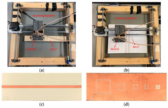
Figure 10.
Main components of the microwave imaging system with: (a) wood with defects as MUT, (b) a pile of paper with copper strips as MUT, (c) front view of the multifrequency near-field sensor, and (d) back view of the multifrequency near-field sensor.
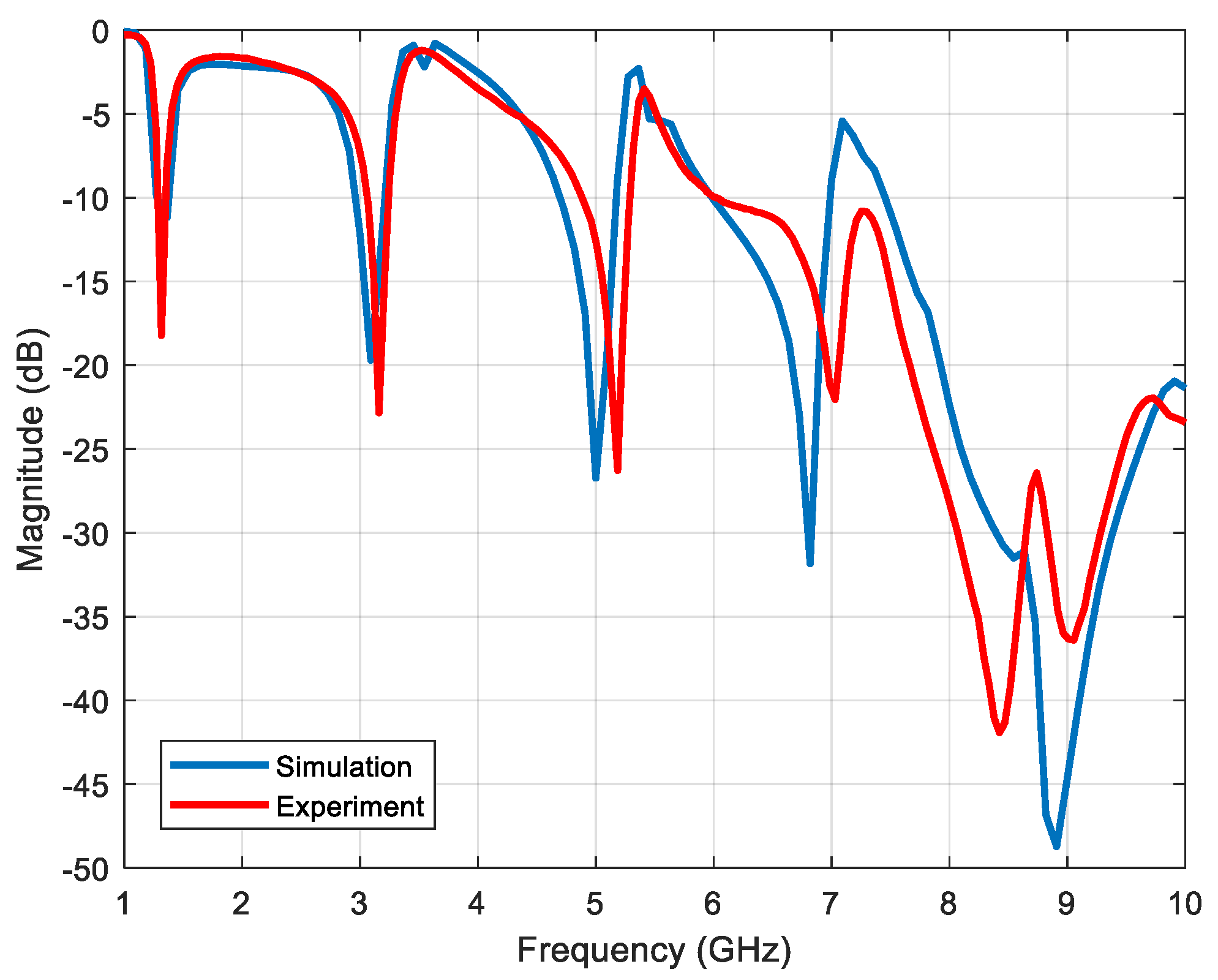
Figure 11 shows the comparison between the simulated and measured for the sensor array when the object is not present. As noted, for experiments, responses of resonating frequencies with the presence of the object are utilized. However, there are six resonant frequencies instead of five within the band of 1 GHz to 10 GHz, due to the coupling of the resonators which are in close proximity. They are at 1.216 GHz, 2.855 GHz, 4.549 GHz, 6.036 GHz, 7.783 GHz, and 9.054 GHz. The slightly different resonant behavior compared to the simulated response of the sensor is due to the use of the shielding box for the sensor array. With that being said, the following results are presented by using five and six resonant frequencies for comparison (when using five frequencies, we discard the data obtained at 7.783 GHz). In addition, similar to the simulation results, for faster data acquisition, we are scanning along one axis only.

Figure 11.
Simulated and measured data without the presence of object.
4.1. Sizing of Defects in Wood
Here, as proof-of-concept, we conduct experiments to detect defects in a piece of wood. The wood is placed under the sensor and the sensor scans the wood piece from −6 cm to 6 cm with 100 steps along the scanning axis. We aim at estimating defects with a depth resolution of 2 mm and with a maximum depth of 6 mm away from the surface of the MUT. Thus, we consider three imaged lines corresponding to depths of 2 mm, 4 mm, and 6 mm. For this purpose, three defects are measured with depths of 2 mm, 4 mm, and 6 mm. Each defect has a width of approximately 1 mm along the scanning axis. To obtain the PSF data corresponding to the depth of 4 mm, the responses obtained for the defect with a depth of 2 mm are subtracted from the responses measured for the defect with a depth of 4 mm. Similarly, to obtain the PSF data corresponding to the depth of 6 mm, the responses obtained for the defect with the depth of 4 mm are subtracted from the responses measured for the defect with a depth of 6 mm.
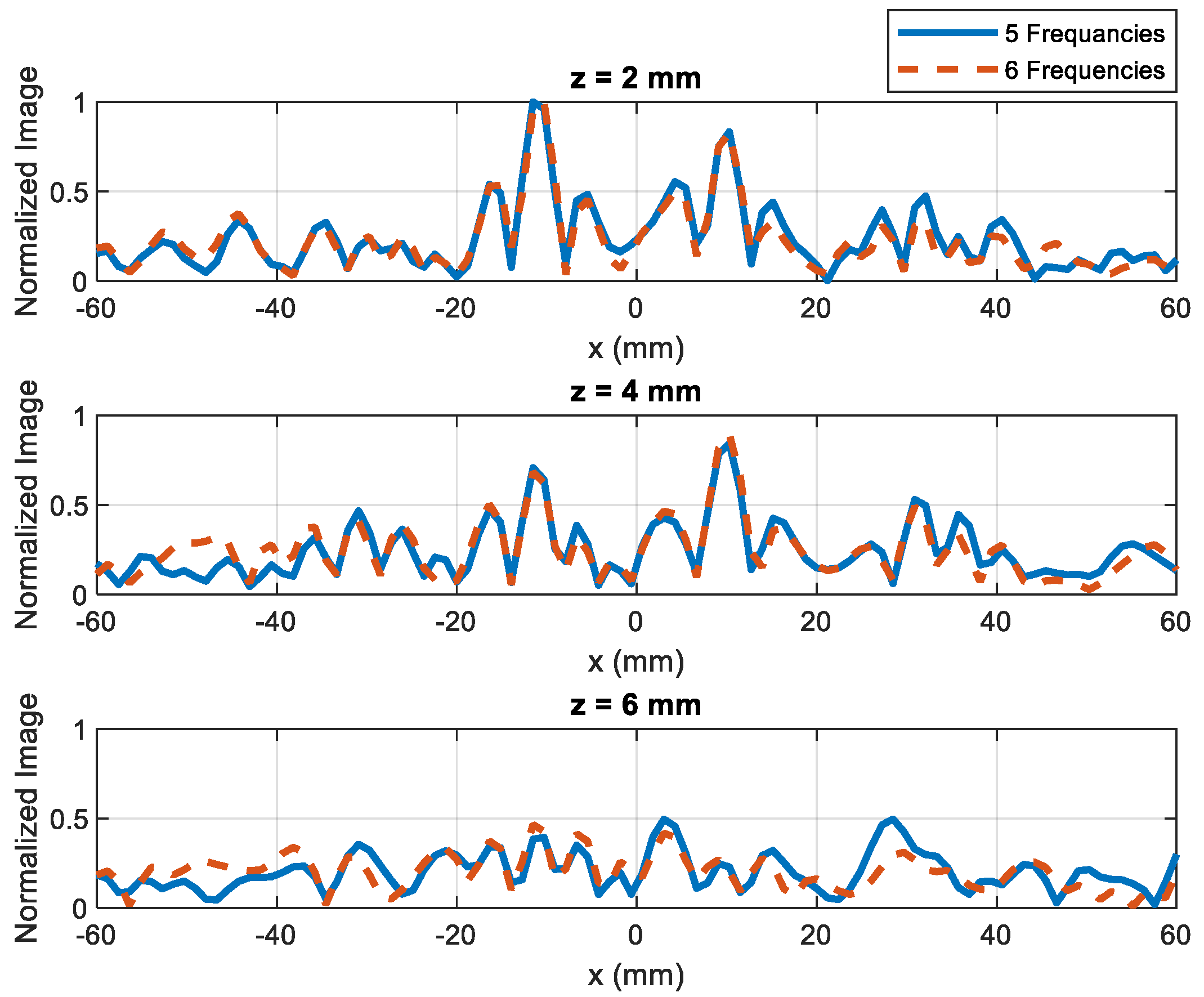
Then for the imaged scenario, two defects with depths of 4 mm are at x = ±10 mm. From the collected responses and applying the proposed method, the reconstructed images are as follows. Figure 12 shows the reconstructed images with five frequencies (discarding the data at 7.783 GHz) and six frequencies. Overall, the defect is distinguishable at z = 2 mm and 4 mm. Moreover, it can be observed that there are no major changes or improvements when using six frequencies.
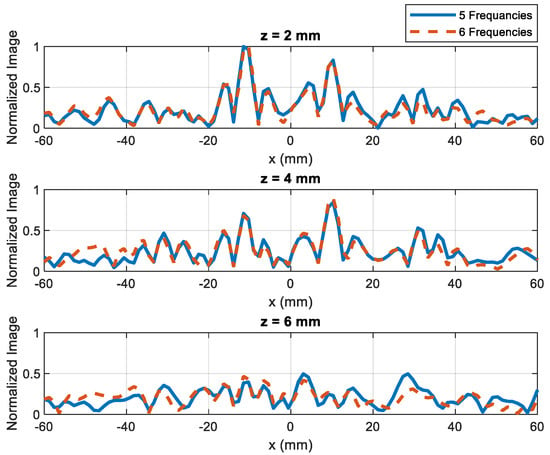
Figure 12.
Reconstructed 1D images of defect with a depth of 4 mm when using 5 and 6 frequencies.
Then, in Figure 13, the estimated thicknesses of the defects are presented for both five and six frequencies when using (12) to combine the 1D images in Figure 12., It is observed that the estimated thicknesses do not differ significantly. Although the estimated depth of the defect value is satisfactorily close to the true value of 4 mm.
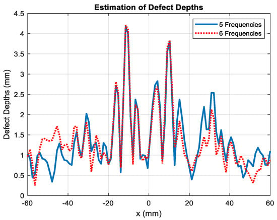
Figure 13.
Thickness estimation of defects with a depth of 4 mm using data at 5 and 6 resonant frequencies.
4.2. Imaging of Hidden Copper Strips
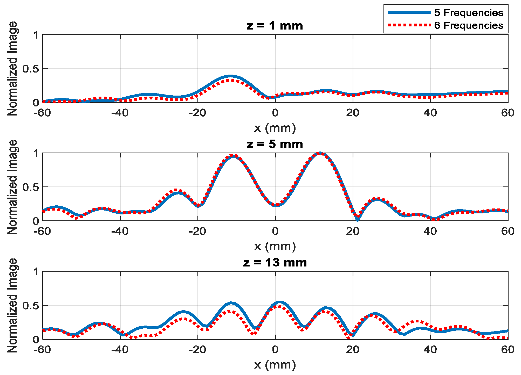
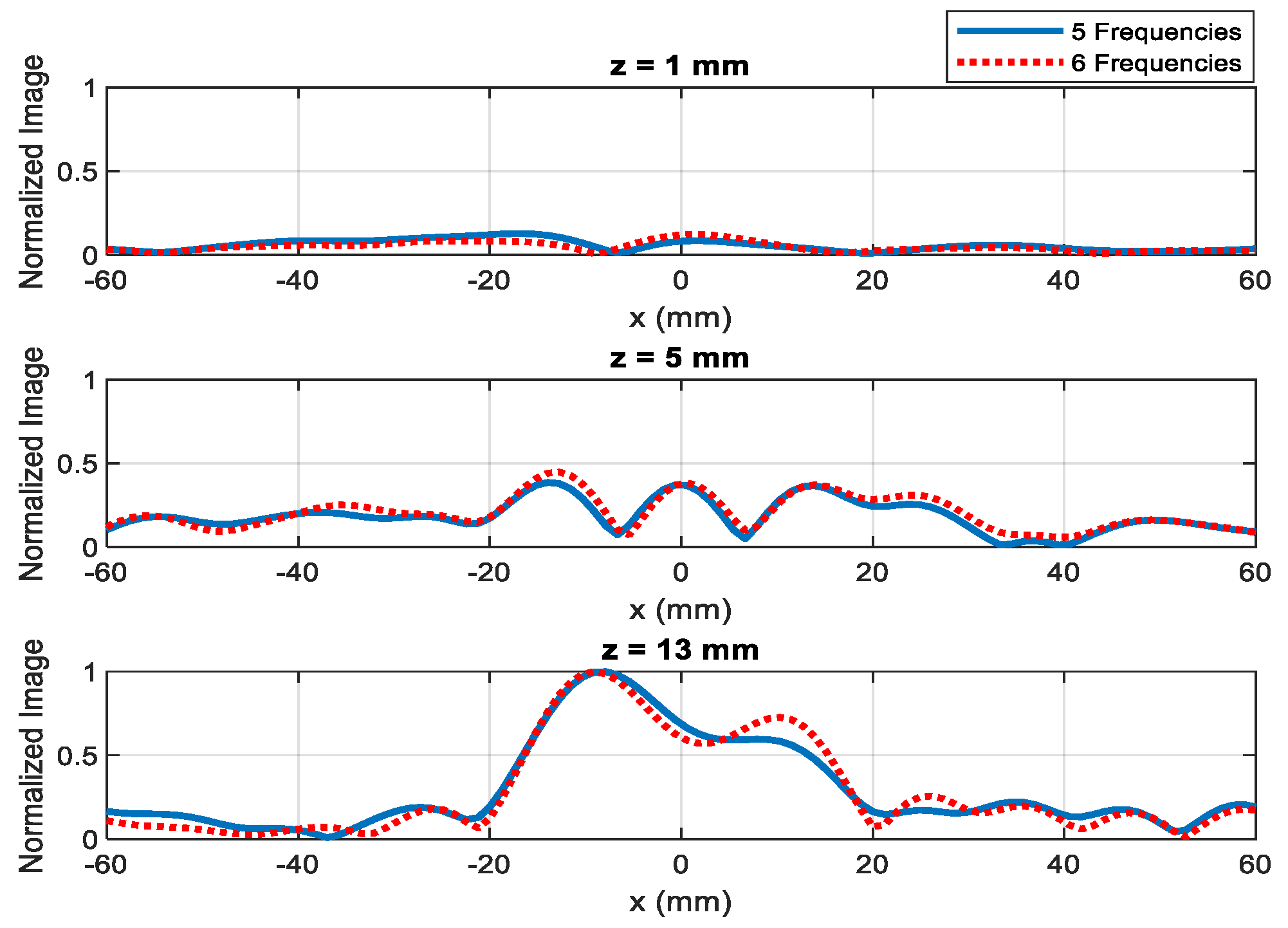
Here, we conduct experiments to image copper strips hidden inside a stack of papers. Similar to the setup for the detection of defects in the wood, the sensor scans the scattered responses above the MUT along the x-axis from −6 cm to 6 cm with 100 steps. Here, the Pos, which are single strips of copper with a width of 2 mm, are measured when they are placed at depths of 1 mm, 5 mm, and 13 mm. This indicates that imaging will be performed at these depths. Then, the test scenarios are created with two copper strips with a width of 2 mm at x = ±10 mm.
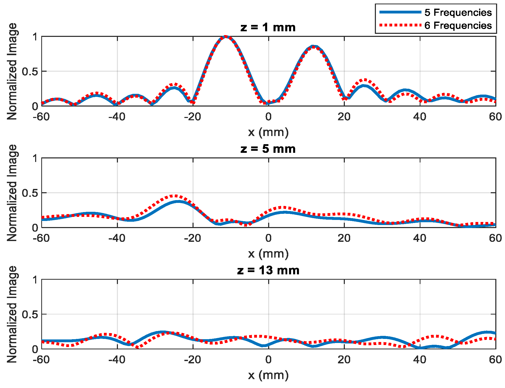
Figure 14, Figure 15 and Figure 16 show the reconstructed 1D images for copper strips placed at depths of 1 mm, 5 mm, and 13 mm and when using data at five and six frequencies. From Figure 14, it can be observed that the reconstructed image shows a clear peak at a depth of 1 mm for both five and six frequencies and there is no significant difference between the results utilizing data at five and six frequencies. Then, for Figure 15, the peaks are clear at a depth of 5 mm. Lastly, for Figure 16, one peak is more obvious compared to the other at a depth of 13 mm. In general, the results for objects at depths of 1 mm and 5 mm are better compared to those at depth of 13 mm. In addition, using six frequencies shows some improvement in the reconstructed image for the objects at depth of 13 mm. To improve this study, a better mechanical system can be built and implemented for imaging to reduce the undesired ripples in the stand-off distance of the sensor. In addition, changing the VNA settings such as increasing the averaging and narrowing the intermediate frequency (IF) bandwidth can improve the results at a cost of increasing the measurement time.
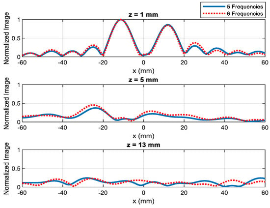
Figure 14.
Reconstructed 1D images for copper strips placed at a depth of 1 mm when using data at 5 and 6 resonant frequencies.
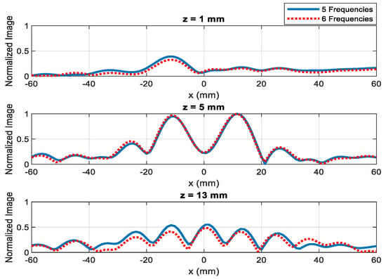
Figure 15.
Reconstructed 1D images for copper strips placed at a depth of 5 mm when using data at 5 and 6 resonant frequencies.
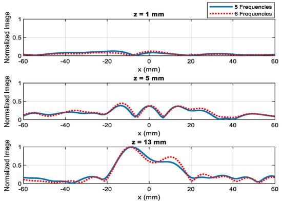
Figure 16.
Reconstructed 1D images for copper strips placed at a depth of 13 mm when using data at 5 and 6 frequencies.
5. Discussion and Conclusions
In this paper, the use of a multifrequency near-field microwave sensor array was extended for imaging dielectric materials with applications in defect size estimation, skin tumor size evaluation, and object imaging. For the first time, postprocessing based on the concept of near-field holographic imaging was applied to the data collected by the near-field microwave sensors to produce high-resolution quantitative images of defects (NDT application) or tumors (biomedical imaging application). This is in contrast to the previous works which normally plot the raw data measured by the near-field microwave sensors to produce images. The comparison of the proposed imaging system with those already described in Section 1 is presented in Table 1. The proposed work here is the only one that achieves depth sizing together with providing high-resolution cross-range images by applying an advanced postprocessing technique. Although without such postprocessing, achieving high accuracy depth estimation is possible (as reported by the previous works), the resolution in the cross-range directions (x- and y-axis) would be degraded.

Table 1.
Comparison of the proposed imaging system with those in the literature.
Regarding the resolution, since the proposed method can process parts of the evanescent wave spectrum, we believe that the resolution is better than the diffraction limit. This can be verified using the simulation study of the defects in the dielectric material. Using Figure 5a, the cross-range resolution for was computed from the 3-dB level of the reconstructed defect plot, leading to a value of around 5 mm while the diffraction limit for the resolution is 13.6 mm and 6.1 mm for the air and dielectric materials, respectively (diffraction limit in the resolution is λ/4, where λ is the wavelength at the center frequency of the band, i.e., 5.5 GHz). In addition, the depth resolution in that simulation study was 2 mm, which is much smaller than the diffraction-limited range resolution of 16.7 mm and 7.5 mm in air and dielectric materials, respectively (diffraction limit in the resolution along the range is c/2B, where c is the speed of light in the medium and B is the bandwidth of the system which is 9 GHz here). However, the detection resolution degrades as the depth increases and this is due to the near-field sensor utilized in this work (evanescent waves decay fast as the distance to the sensor increases). Furthermore, as a near-field imaging probes, the imaging depth is limited due to the capability to measure the evanescent waves up to a short range.
Here, we present the Q factor computed from the simulated data. As noted, to get better accuracy of the Q factor, we simulated the structure around each of the five resonating frequencies individually with fine frequency sampling. For the five resonant frequencies at 1.343 GHz, 3.116 GHz, 5.035 GHz, 6.815 GHz, and 8.875 GHz, the Q factors using the 3-dB bandwidth were 149.22, 173.11, 419.583, 141.979, and 59.167, respectively. The Q factor influences the sensor resolution as a higher Q factor leads to a sharper resonance and higher sensitivity for detecting smaller objects and defects.
As mentioned, resolution and Q factor can both be improved through different methods and implementations. Better resolution can be obtained by reducing the standoff distance between the sensor and imaged medium. This allows for measuring a larger portion of the evanescent wave spectrum, which alternatively leads to better cross-range resolutions as is well-known in microwave microscopy [24]. Another method to improve the resolution is through sensor design. In [25], four hexagonal-shaped CSRR components arranged in a honey-cell configuration have been employed to achieve impressive detection capability which is due to the highly concentrated electromagnetic fields around the sensed region. A similar focusing method can be utilized to improve the imaging results in the proposed technique. Other than reducing standoff distance or using another sensor design for better resolution, one can also apply superoscillartory filters to the reconstructed images [26] to improve the resolution. For the improvement of the Q factor, a circular CSRR design can be implemented for imaging purposes. In [27], the comparison between a circular and rectangular CSRR has been made and it has been shown that a circular CSRR has a higher Q factor compared to a rectangular CSRR. Along with implementing a circular CSRR, the implementation of substrate integrated waveguide (SIW) can also achieve higher Q factors [28].
For fast proof-of-concept demonstrations, 1D scanning and imaging were presented here, although the theory was presented for two-dimensional (2D) scenarios. Thus, extending the results for 2D imaging is straightforward, though time consuming.
The simulation study was split into two parts, the assessment of defects in dielectric materials and the evaluation of skin tumor size. For the first study, it was observed that the accuracy of depth estimation degrades as the depth of defects increases. This is due to the use of Born approximation in deriving the imaging algorithm. Furthermore, from the simulation study for skin tumor size estimation, it can be concluded that the tumor depth can be estimated satisfactorily. The results show that smaller tumors closer to the skin surface can be sized more precisely compared to the cases of evolving tumors.
Next, we conducted two experimental studies. For proof of concept, wood was used in the first study. We were able to detect and estimate the depth of the defects in the wood with a high precision. Furthermore, there were no significant changes when using the data at five or six resonating frequencies. In addition, we also included a study of hidden object detection using copper strips. It was observed that hidden copper strips at 1 mm and 5 mm were more detectable compared to the farthest one at 13 mm.
In general, we can conclude that the proposed NDT technique can be employed for both defect depth estimation and object imaging with applications in NDT, biomedical imaging, and multilayered PCB evaluation.
Author Contributions
Conceptualization, R.K.A. and M.R.; methodology, R.K.A. and M.R.; software, Y.G. and R.K.A.; validation, Y.G. and R.K.A.; formal analysis, Y.G. and R.K.A.; investigation, Y.G. and R.K.A.; resources, R.K.A. and M.R.; data curation, Y.G.; writing—original draft preparation, Y.G.; writing—review and editing, Y.G. and R.K.A.; visualization, Y.G.; supervision, R.K.A. and M.R.; project administration, R.K.A. and M.R.; funding acquisition, R.K.A. and M.R. All authors have read and agreed to the published version of the manuscript.
Funding
This research was funded by US National Science Foundation (NSF), grant number 1920098.
Institutional Review Board Statement
Not applicable.
Informed Consent Statement
Not applicable.
Data Availability Statement
Not applicable.
Conflicts of Interest
The authors declare no conflict of interest.
References
- Kharkovsky, S.; Zoughi, R. Microwave and millimeter wave nondestructive testing and evaluation—Overview and recent advances. IEEE Instrum. Meas. Mag 2007, 10, 26–38. [Google Scholar] [CrossRef]
- Bhat, B.N. Aerospace Materials and Applications; American Institute of Aeronautics and Astronautics: Reston, VA, USA, 2018; pp. 154–196. [Google Scholar]
- Ghasr, M.; Kharkovsky, S.; Zoughi, R.; Austin, R. Comparison of near-field millimeter-wave probes for detecting corrosion precursor pitting under paint. IEEE Trans. Instrum. Meas. 2005, 54, 1497–1504. [Google Scholar] [CrossRef]
- Samsingh, V.R.; Subbaraj, S.; Malathi, K.; Sundarsingh, E.F.; Yogeshwari, P.; Saffrine, K.; Rao, Y.R. Characterization of delamination in fiber-reinforced epoxy-based PCB laminates, using an EBG-enhanced planar microwave sensor. IEEE Trans. Compon. Packag. Manuf. Technol. 2017, 7, 1739–1746. [Google Scholar] [CrossRef]
- Samsingh, V.R.; Kanagasabai, M.; Sundarsingh, E.F. A novel metamaterial enhanced microwave testing system for bare PCB substrates using image rendering approach. IEEE Trans. Compon. Packag. Manuf. Technol. 2017, 7, 285–291. [Google Scholar] [CrossRef]
- Töpfer, F. Micromachined Microwave Sensors for Non-Invasive Skin Cancer Diagnostics. Ph.D. Thesis, KTH Royal Institute of Technology, Stockholm, Sweden, 2019. [Google Scholar]
- Mirbeik-Sabzevari, A.; Li, S.; Garay, E.; Nguyen, H.T.; Wang, H.; Tavassolian, N. Synthetic ultra-high-resolution millimeter-wave imaging for skin cancer detection. IEEE Trans. Biomed. Eng. 2019, 66, 61–71. [Google Scholar] [CrossRef]
- Shafi, K.T.M.; Abou-Khousa, M.A. Super-resolution microwave imaging using small loop loaded with spiral resonator. In Proceedings of the 2017 IEEE SENSORS, Glasgow, UK, 29 October–1 November 2017; pp. 1–3. [Google Scholar]
- Mukherjee, S.; Shi, X.; Udpa, L.; Udpa, S.; Deng, Y.; Chahal, P. Design of a split-ring resonator sensor for near-field microwave imaging. IEEE Sens. J. 2018, 18, 7066–7076. [Google Scholar] [CrossRef]
- Lee, C.S.; Yang, C.L. Thickness and permittivity measurement in multi-layered dielectric structures using complementary split-ring resonators. IEEE Sens. J. 2014, 14, 695–700. [Google Scholar] [CrossRef]
- Ali, A.; El Badawe, M.; Ramahi, O.M. Microwave imaging of subsurface flaws in coated metallic structures using complementary split-ring resonators. IEEE Sens. J. 2016, 16, 6890–6898. [Google Scholar] [CrossRef]
- Govind, G.; Tiwari, N.K.; Agrawal, K.K.; Akhtar, M.J. Microwave subsurface imaging of composite structures using complementary split ring resonators. IEEE Sens. J. 2018, 18, 7442–7449. [Google Scholar] [CrossRef]
- Amineh, R.K.; Ravan, M.; Sharma, R. Nondestructive testing of nonmetallic pipes using wideband microwave measurements. IEEE Trans. Microw. Theory Tech. 2020, 68, 1763–1772. [Google Scholar] [CrossRef]
- Wu, H.; Ravan, M.; Sharma, R.; Patel, J.; Amineh, R.K. Microwave holographic imaging of nonmetallic concentric pipes. IEEE Trans. Instrum. Meas. 2020, 69, 7594–7605. [Google Scholar] [CrossRef]
- Shah, M.B.; Gao, Y.; Ravan, M.; Amineh, R.K. Quantitative defect size evaluation in fluid-carrying nonmetallic pipes. IEEE Trans. Microw. Theory Tech. 2022, 70, 4071–4081. [Google Scholar] [CrossRef]
- Ma, X.; Liu, Q.; Yu, N.; Xu, D.; Kim, S.; Liu, Z.; Jiang, K.; Wong, B.M.; Yan, R.; Liu, M. 6 nm super-resolution optical transmission and scattering spectroscopic imaging of carbon nanotubes using a nanometer-scale white light source. Nat. Commun. 2021, 12, 6868. [Google Scholar] [CrossRef] [PubMed]
- Kim, S.; Yu, N.; Ma, X.; Zhu, Y.; Liu, Q.; Liu, M.; Yan, R. High external-efficiency nanofocusing for lens-free near-field optical nanoscopy. Nat. Photonics 2019, 13, 636–643. [Google Scholar] [CrossRef]
- Zhang, K.; Amineh, R.K.; Dong, Z.; Nadler, D. Microwave sensing of water quality. IEEE Access 2019, 7, 69481–69493. [Google Scholar] [CrossRef]
- Amineh, R.K.; Ravan, M.; Khalatpour, A.; Nikolova, N.K. Three-dimensional near-field microwave holography using reflected and transmitted signals. IEEE Trans. Antennas Propag. 2011, 59, 4777–4789. [Google Scholar] [CrossRef]
- Amineh, R.K.; McCombe, J.J.; Khalatpour, A.; Nikolova, N.K. Microwave holography using point-spread functions measured with calibration objects. IEEE Trans. Instrum. Meas. 2015, 64, 403–417. [Google Scholar] [CrossRef]
- Altair FEKO. Available online: https://www.altair.com/feko/ (accessed on 1 November 2022).
- Mirbeik-Sabzevari, A.; Ashinoff, R.; Tavassolian, N. Ultra-Wideband Millimeter-Wave Dielectric Characteristics of Freshly Excised Normal and Malignant Human Skin Tissues. IEEE Trans. Biomed. Eng. 2018, 65, 1320–1329. [Google Scholar] [CrossRef]
- Boparai, J.; Popović, M. Development and Characterization of Skin Phantoms at Microwave Frequencies. IEEE J. Electromagn. RF Microw. Med. Biol. 2022, 6, 296–304. [Google Scholar] [CrossRef]
- Tabib-Azar, M. Microwave microscopy and its applications. AIP Conf. Proc. 2001, 557, 400. [Google Scholar]
- Omer, A.E.; Shaker, G.; Safavi-Naeini, S.; Kokabi, H.; Alquié, G.; Deshours, F.; Shubair, R.M. Low-cost portable microwave sensor for non-invasive monitoring of blood glucose level: Novel design utilizing a four-cell CSRR hexagonal configuration. Sci. Rep. 2020, 10, 15200. [Google Scholar] [CrossRef] [PubMed]
- Amineh, R.K.; Eleftheriades, G.V. 2D and 3D sub-diffraction source imaging with a superoscillatory filter. Opt. Express 2013, 21, 8142–8156. [Google Scholar] [CrossRef] [PubMed]
- Ansari, M.A.H.; Jha, A.K.; Akhtar, M.J. Design and Application of the CSRR-Based Planar Sensor for Noninvasive Measurement of Complex Permittivity. IEEE Sens. J. 2015, 15, 7181–7189. [Google Scholar] [CrossRef]
- Memon, M.U.; Lim, S. Microfluidic High-Q Circular Substrate-Integrated Waveguide (SIW) Cavity for Radio Frequency (RF) Chemical Liquid Sensing. Sensors 2018, 18, 143. [Google Scholar] [CrossRef] [PubMed]
Disclaimer/Publisher’s Note: The statements, opinions and data contained in all publications are solely those of the individual author(s) and contributor(s) and not of MDPI and/or the editor(s). MDPI and/or the editor(s) disclaim responsibility for any injury to people or property resulting from any ideas, methods, instructions or products referred to in the content. |
© 2023 by the authors. Licensee MDPI, Basel, Switzerland. This article is an open access article distributed under the terms and conditions of the Creative Commons Attribution (CC BY) license (https://creativecommons.org/licenses/by/4.0/).

