1. Introduction
The revolution of the Internet of Things (IoT) connected era enables an endless field to invent new applications for tracking devices, intelligent sensors and agriculture, smart home, etc. The connectivity, range, and battery longevity of those devices depend upon antennas.
Antennas for wireless devices mainly rely on shaping the geometry of the antenna to make them small enough to fit in the device and multiband to provide operation across several frequency bands [
1,
2,
3,
4,
5,
6,
7,
8,
9,
10]. Spiral, meander, and loops are typical for designing an antenna to a particular frequency. In [
11], a meandered monopole is proposed for a mobile phone. Although the bandwidth is 101.7%, the size is too big (100 mm × 44 mm, 0.3 λ at 900 MHz) to fit in a small IoT device (
Table 1). In [
12], a spiral monopole is proposed for covering 900 MHz, 1800 MHz, and 2200 MHz, having a size of 24 mm × 22.75 mm (λ/14 at 900 MHz). In [
13], a meandered monopole is designed for 900 MHz, with a large size of 42.2 mm × 70 mm (0.21 λ at 900 MHz). In [
14], a multi-spiral monopole is analysed for 900 MHz, with a size of 22.9 mm × 10 mm (λ/14 at 900 MHz). In some cases, a simple matching network comprising lumped components such as capacitors and inductors is used for fine-tuning the frequency response of the antenna. Other cases use a tuneable component, such as a digitally tuneable capacitor with a meandered monopole of a compact size of 20 mm × 18 mm [
15].
A different approach is addressed by antenna boosters, a tiny non-resonant element, where the frequencies of operation are easily adjusted thanks to a matching network [
16]. Such a design is addressed with matching network synthesis tools available in microwave simulators [
17,
18,
19].
The paper compares a classic spiral monopole antenna and an antenna booster when operating at 900 MHz in a reference 120 mm × 60 mm ground plane. Then, the size of the ground plane is changed while keeping both antenna systems the same. The objective is to compare the reusability of both antenna designs for a wide set of ground planes. In the end, the higher the reusability, the simpler the antenna technique is for device designers, since a particular design can be reused across a wide set of cases without any further change in the antenna part, either in the antenna geometry or in the matching network. This is a novel way of comparing antenna technologies since most of the prior art focuses only on a given antenna in a particular device size. As a result, a new figure of merit is proposed, called reuse, which quantifies how much an antenna element can be reused according to a specific parameter. In this case, the reference parameter is an S11 < −6 dB, as elaborated in the next sections.
This paper is structured as follows: The two antenna types are compared in
Section 2. In
Section 3, both antenna types are studied for different ground planes, from a small size of 20 mm × 30 mm to a big size of 200 mm × 200 mm. Then, a prototype for the antenna booster is fabricated and tested to validate the numerical analysis. Next, a discussion is given in
Section 4. Finally,
Section 5 concludes.
2. Antenna Booster and Monopole Antenna Designs
The aim is to compare the performance of the antenna booster technology and a monopole antenna under the same challenging conditions. In order to create these conditions, the clearance area of the ground plane is reduced to only 20 mm × 11 mm, so the extra 40 mm × 11 mm ground plane area could be used for other purposes, such as integrating more electronics. The frequency range is the ISM 863–928 MHz.
Before comparing the antenna booster and the monopole antenna, it is worth mentioning some characteristics of an antenna booster. An antenna booster is an electrically small conductive parallelepiped, typically less than λ/20 at the lowest frequency of operation, where the correct location on a ground plane of a PCB (Printed Circuit Board) enables the excitation of currents and, as a result, achieves bandwidth and efficiency. Since it is electrically small, its impedance nature is reactive and capacitive. Therefore, a matching network is added to provide impedance matching. This fact offers flexibility since the matching network allows the designer to provide single-band or multiband operation to the device. Moreover, the design of a matching network is easily addressed by network synthesis, which makes the design process easy and fast, and it looks more like a microwave problem than an antenna design [
17]. It is worth mentioning that such excitation of currents depends on the position of the antenna booster on the ground plane [
17], the corner being the preferred position. Either way, such excitation has no impact on the electronics, for example, on the sensitivity of the device compared to a classic monopole antenna [
20]. In fact, currents on the ground plane are also excited by other antennas, such as PIFA. The advantage is that those currents can be excited by an antenna booster that is ten times smaller.
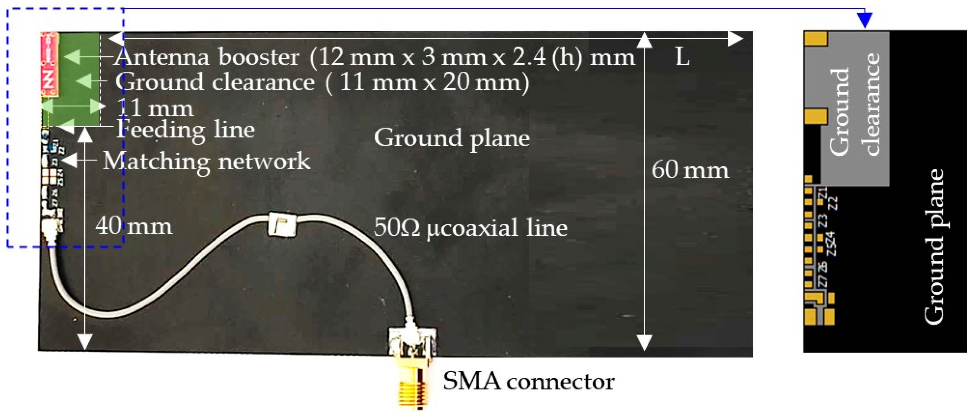
Firstly, the antenna booster and monopole antenna designs have been simulated with a reference ground plane size of 120 mm × 60 mm + 40 mm × 11 mm printed on an FR4 (Flame Retardant #4 epoxy) substrate, commonly employed in PCBs due to its competitive price (
Figure 1) [
21]. Electromagnetic simulations are performed with MoM (Method of Moments) software (IE3D). Once both designs have been adjusted for operation for the reference ground plane, different ground planes ranging from 20 mm × 30 mm to 200 mm × 200 mm (using steps of 10 mm) are going to be tested with the same antenna and matching network to see how many could be reused with the same design, without having to redo the design for each size.
The antenna design for the monopole antenna was obtained by adding a λ/4 monopole to the ground plane and modifying its length to make it fit into the frequency band. The feeding point was placed on the added part of the ground plane to allow more bandwidth. Nevertheless, it was insufficient to match the band, so a matching network had to be added to fine-tune the impedance (
Figure 1a). The matching network is a shunt inductor of value 8 nH (0402 SMD component, Q = 67 at 900 MHz).
As mentioned, the one-component matching network allows the impedance curve of the monopole antenna to stay below −6 dB, which is the minimum required.
The second antenna design was based on the antenna booster technology [
16,
22]. Since the antenna booster is a non-resonant element, a matching network adds the flexibility to easily match the antenna system at the desired frequency [
17]. Furthermore, since it is a single-band case, the matching network is simple, consisting of only two inductors (
Figure 1b). This case consists of a series inductor of 39 nH and a shunt inductor of 18 nH (Q > 80) (
Figure 2). The feeding point is at the exact location of the monopole antenna, having the same 20 mm × 11 mm clearance area.
Since the impedance of the antenna booster is capacitive, a series and a shunt inductor are used to match the antenna booster. As a result, the achieved bandwidth is BW = 17.4%, 1.8 times the bandwidth achieved by the monopole antenna occupying the same clearance area (
Figure 3,
Table 2).
To summarise the results of the antenna designs: they both accomplish 863–928 MHz. However, the antenna booster bandwidth is larger, making it more attractive since it can allocate more radio protocols beyond the 863–928 MHz frequency range. The bandwidth of both cases has been compared with bandwidth potential [
23], with Optenni Lab results showing good agreement. Bandwidth potential considers the bandwidth an antenna can obtain with a simple matching network of one or two components. Having the antenna booster with more bandwidth enables a further reduction of the ground clearance area, which will imply only a new matching network. However, for the monopole antenna, a new antenna should be designed.
The following section analyses the impact of varying the ground plane size while keeping the same matching network. The purpose is to study the design reuse for other platforms without changing the matching network or the antenna part.
3. Analysis of the Reuse of the Antenna Systems for Different Ground Plane Sizes
The size of the ground plane is changed from a small one of 20 mm × 30 mm to 200 mm × 200 mm while keeping the same clearance area for both cases, being the same as the one for the reference 120 mm × 60 mm ground plane. The total number of ground planes is 342.
The worst reflection coefficient within the 863–928 MHz range is stored for each ground plane and then represented in a 2D plot. These results have been displayed in a thermal graph, where the warmer colours mean poor matching, and the cooler ones mean better matching (S
11 ≤ −6 dB). Moreover, the edge with S
11 = −6 dB is defined using a black line (
Figure 4). The ground planes providing an S
11 ≤ −6 dB within 863–928 MHz are within the area inside the contours defined in
Figure 4, called the
cluster.
3.1. On the Reuse: The Cluster
Remarkably, the antenna booster is well-matched (S
11 ≤ −6 dB) with many more different ground plane sizes than the monopole antenna (
Figure 4,
Table 3): the antenna booster can be reused across 53.8% cases, whereas the monopole antenna can be only reused 4.6%. For example, if the original 120 mm × 60 mm ground plane is reduced to 90 mm × 60 mm, the antenna booster maintains an S
11 ≤ −6 dB across 863–928 MHz, whereas the monopole antenna degrades to −4 dB. It is clearly shown from the cluster shapes (
Figure 4) that the antenna booster is robust to ground plane changes, whereas the monopole is sensitive to changes.
The shape of the impedance cluster of the antenna booster is interesting, where it can be extrapolated to a cross delimited by the −6 dB curve since the antenna is matched inside this zone. Moreover, as mentioned earlier, the reference case was designed on a 120 mm × 60 mm ground plane, which is why the coldest zones (better matching) are where L = 120 mm and W = 60 mm or vice versa, resulting in a symmetric cluster along the L = W line. The worst ground plane sizes are those in the corners, except the top right corner. The top left (large widths) and the bottom right (large lengths) parts, although not providing an S
11 < −6 dB with the current Lseries-Lshunt matching network, can be matched using a different matching network. However, the most critical area is the bottom left corner which includes electrically small ground planes. Further discussion on the off-cluster zones (Zone #1, 2, 3) can be found in [
24]. In particular, Zone #1 and #3 need a different matching topology (antenna booster connected to a series L and shunt C). Zone #2 (small PCB) requires special treatment since the bandwidth decreases when the ground plane becomes smaller. Therefore, broad-banding mechanisms or reconfigurable solutions are needed to achieve bandwidth.
The total efficiency is computed for each ground plane size (
Figure 5). Total efficiency considers both matching and radiation efficiency (η
r) as follows, η
t = η
r(1 − |S
11|
2), and represents the ratio of the radiated power to space over the incoming power to the antenna system. The simulation considers the losses due to the loss tangent of the substrate, the losses of the matching network, and the radiation efficiency of each antenna system on its respective ground plane size. The same matching network, as shown in
Figure 1, is used. The total efficiency is superior for the antenna booster case. For example, for a 20 mm × 80 mm ground plane size, the antenna booster is 2.3 dB above the efficiency of the monopole.
Other values for different ground plane sizes are shown in
Table 4. Besides this superior efficiency of the antenna booster compared to the monopole antenna, the better impedance matching when connecting the antenna booster to a transceiver ensures output power close to the nominal. Therefore, a side effect of mismatching besides total efficiency is its impact on the output power of the transceiver. As reflected in
Figure 4, the antenna booster is more robust also in this regard, as the reuse ratio reflects.
The present result showing the better performance of the antenna booster compared to a monopole for small ground plane clearance is aligned with a different analysis where the same antenna booster presented here (12 mm × 3 mm × 2.4 mm) was compared for multiband performance to a large 96 mm × 21 mm FPC (Flexible Printed Circuit) antenna. The conclusions of [
25] were the superior performances in measured total efficiency for a small (65 mm × 42 mm), medium (95 mm × 42 mm), and large PCB (131 mm × 60 mm).
3.2. Physical Validation
After obtaining the results from the theoretical study, an experimental validation was conducted to validate the simulations (
Figure 6). Two cases were fabricated and tested: the reference 120 mm × 60 mm ground plane and the 100 mm × 60 mm size. According to
Figure 4, the 100 mm × 60 mm is within the cluster, and thus, S
11 should be less than −6 dB across 863–928 MHz. The measured data confirm this fact (
Figure 7).
Moreover, the total antenna efficiency (η
t) of the simulated and measured antenna is also displayed in
Figure 8, showing good agreement. The simulated total efficiency across 863–928 MHz is 84%, while the measured is 76%, representing a 0.4 dB discrepancy, which is tolerable. Total efficiency is measured in the anechoic chamber using 3D pattern integration with MVG StarLab 18. Regarding realised gain, it reaches 2.8 dBi at 900 MHz, showing an omnidirectional pattern at XZ (φ = 0° plane) and a drop along the long axis of the ground plane (±y direction). The radiation pattern is similar to a half-wavelength dipole, which is a consequence of the currents on the ground plane, which are aligned along the
Y-axis for this ground plane size. This radiation pattern is convenient for IoT devices since the device receives almost equally from any direction of the incoming electromagnetic signal.
4. Discussion
Besides the previous advantages shown above, it is interesting to discuss the impact of the permittivity of the FR4 substrate since it may vary from manufacturer to manufacturer or due to temperature and humidity conditions [
26]. In this case, the relative permittivity of the substrate of the PCB has been changed from the original 4.15 value to 4.7 while keeping everything else the same, including the matching networks (
Figure 9).
The S11 response for both the monopole antenna and antenna booster shift, as expected, to lower frequencies. However, the shifting is more accentuated for the monopole antenna, being 2.3% compared to 1.3% for the antenna booster. The reason is that the monopole antenna is more sensitive to changes in the permittivity of the substrate where the antenna is printed since it alters the coupling between the conductive parts of the antenna. However, the antenna booster being a single conductive element, it is more robust to substrate changes.
The main features of the monopole antenna compared to the antenna booster are gathered in
Table 5. It is remarkable that in addition to the higher reuse of the antenna booster compared to the monopole antenna, the antenna booster can be reused if the ground clearance is further reduced. Since the antenna booster is only 12 mm × 3 mm × 2.4 mm, ground plane clearance can still be reduced. We must bear in mind that reducing the ground clearance reduces bandwidth. Still, as long as the bandwidth is enough for the application, such reduction may enable a larger integration of other components on the PCB. This is not the case for the monopole antenna. If the ground clearance reduces, the design process must start from scratch. For example, when the ground clearance is reduced from 20 mm × 11 mm (242 mm
2) to 15 mm × 9 mm (135 mm
2) for the reference 120 mm × 60 mm ground plane, the bandwidth of the antenna booster decreases from 17.4% to 11.5%. Although smaller, it is still better than the monopole antenna on the original clearance.
5. Conclusions
A monopole antenna and an antenna booster have been compared when operating at 863 MHz to 928 MHz. Both solutions present an S11 ≤ −6 dB on this specific frequency band on the reference 120 mm × 60 mm ground plane. However, the antenna booster features more bandwidth at 900 MHz: 17.4% for the antenna booster compared to 9.5% for the monopole antenna. Therefore, the antenna booster can absorb new radio protocols beyond those in the 863–928 MHz frequency band.
Besides more bandwidth, another advantage of the antenna booster over the monopole antenna is its robustness to ground plane variations. A total of 342 ground planes ranging from 20 mm × 30 mm to 200 mm × 200 mm with increments of 10 mm have been used to analyse the performance of the monopole antenna and antenna booster. In all cases, the antenna set-up is the same: same antenna element and same matching network. The conducted analysis shows that the antenna booster can be reused 53.8%, whereas the monopole antenna only 4.6% (only for ground planes similar to the 120 mm × 60 mm reference ground plane). For example, the antenna booster system can be reused for ground planes with 90 mm ≤ L ≤ 150 mm and 30 mm ≤ W ≤ 200 mm, 20 mm ≤ L ≤ 90 mm and 110 mm ≤ W ≤ 160 mm, and 160 mm ≤ L ≤ 200 mm and 120 mm ≤ W ≤ 200 mm. However, the monopole antenna can be reused for 110 mm ≤ L ≤ 130 mm and 30 mm ≤ W ≤ 90 mm, which is very limited compared to the antenna booster.
The antenna booster is also more robust to variations of the permittivity of the substrate due to different FR4s or changes in humidity or temperature affecting the permittivity. In this regard, when the relative permittivity changes from 4.15 to 4.7, the S11 response for the monopole antenna shifts 2.3% to lower frequencies, whereas the antenna booster is only 1.3%.
Keeping the bill of materials the same (same antenna booster and same matching network) reduces the time to design IoT devices and simplifies procurement and logistics.


