Article

An Enhanced Detection Method of PCB Defect Based on Improved YOLOv7

School of Information Management, Beijing Information Science and Technology University, Beijing 100192, China
*
Author to whom correspondence should be addressed.
Electronics 2023, 12(9), 2120; https://doi.org/10.3390/electronics12092120
Submission received: 24 February 2023 / Revised: 27 April 2023 / Accepted: 4 May 2023 / Published: 6 May 2023

Abstract

:
Printed circuit boards (PCBs) are a critical component of modern electronic equipment, performing a crucial role in the electronic information industry chain. However, accurate detection of PCB defects can be challenging. To address this problem, this paper proposes an enhanced detection method based on an improved YOLOv7 network. First, the SwinV2_TDD module is proposed, which adds a convolutional layer to extract the local features of the PCB. Then, the Magnification Factor Shuffle Attention (MFSA) mechanism is introduced, which adds a convolutional layer to each branch of the Shuffle Attention (SA) to expand its depth and enhance the adaptability of the attention mechanism. The SwinV2_TDD module and MFSA mechanism are integrated into the YOLOv7 network, replacing some ELAN modules and changing the activation function to Mish. The evaluation indexes used are Precision (P), Recall (R), and mean Average Precision (mAP). Experimental results show that the enhanced method achieves an AP of 98.74%, indicating a significant improvement in PCB defect detection performance.

1. Introduction

The printed circuit board (PCB) holds immense importance in the electronic industry as a crucial component for the development of electronic products. PCBs are becoming increasingly integrated and smaller [1] due to the excellent craftsmanship, precise wiring, and rapid development of integrated circuits. However, with the reduction in size, defects in the PCBs are also getting smaller and more challenging to detect. Therefore, it is imperative to conduct a thorough defect detection process during PCB-related production to improve product quality and reduce company costs.
The conventional methods of detecting defects in PCBs are classified into three categories: manual visual inspection, electrical testing, and optical inspection [2]. Manual visual inspection involves workers inspecting bare PCBs directly using their eyes and other equipment. However, this method has become inadequate due to the increasing demand for higher precision in PCB development, as it has poor detection stability and low efficiency. On the other hand, electrical testing employs contact testing to detect defects in bare PCBs, which requires complex testing circuits, expensive molds, and fixtures for each batch of PCBs. This method is also limited in detecting multi-layer PCBs and poses a risk of secondary damage. In contrast, automated optical inspection (AOI) is a non-contact inspection method that uses machine vision technology and image processing algorithms [3]. Industrial cameras capture images of the PCBs, which are transmitted to a computer that provides feedback on the defect detection results. AOI is more stable and accurate than the previous methods, with a faster detection speed [4], and does not impact the PCB.
The advancement of deep learning has led to the development of contactless automatic detection methods, which have become a popular area of research due to their strong recognition adaptability and generalization ability. Typically, deep learning-based detection networks can be categorized into one-stage and two-stage networks. The one-stage network includes Single Shot Detector (SSD) [5], and You Only Look Once (YOLO) [6]. In contrast, the two-stage network includes regions with convolutional neural networks (R-CNN) [7], Fast R-CNN [8], and Faster R-CNN [9], which is an improved version of R-CNN. The primary difference between these networks is that the one-stage network directly predicts the location and category of defects in the network after feature extraction, while the two-stage network first generates proposals that may include defects, then conducts the detection process. Specifically, the two-stage network generates candidate boxes of different sizes that may contain defect features, then performs target detection to predict defect classes and locations. However, the detection speed is slow due to the generation of many candidate frames. On the other hand, the one-stage network performs both training and detection in a single network without the need for explicit region proposals, resulting in faster detection speed. This paper adopts the one-stage network based on YOLOv7 [10] and improves it to meet real-time performance requirements in the industrial field.
The Swin Transformer v2 [11] is designed to overcome three significant challenges in large visual model training and application, namely, model instability, the resolution gap problem, and a chronic lack of labeled data. To address these challenges, the Swin Transformer v2 proposes three primary methods. First, it combines cosine attention and post-normalization to enhance model stability. Second, it introduces a logarithmic space continuous location deviation method, which enables the model to be trained on low-resolution images, then transferred to its higher-resolution counterparts. Lastly, it introduces SimMIM, a self-supervised pretraining method that reduces the need for large amounts of labeled data. To improve the global feature extraction and stability of the model, SwinV2_CSPB modules can replace some ELAN modules in the YOLOv7 backbone network.
The attention mechanism is a widely used method to enhance model performance. Typically, attention weight is obtained by calculating the importance of each position in the input sequence. Shuffle Attention (SA) [12] improves upon this method by shuffling and reordering the input sequence, then calculating the importance of each position to obtain the attention weight. Compared with the traditional attention mechanism, it increases computational efficiency by using a new calculation method that reduces the amount of computation required to calculate attention weight. Additionally, SA can enhance the model’s generalization ability, resulting in more consistent performance on both training and test data.
The main contributions of this paper are as follows:
(1) The Swin Transformer v2 has been further enhanced with the SwinV2_TDD (Tiny Defect Detection) structure, which involves adding a convolutional layer and an upsampling layer at the beginning of each stage in the Swin Transformer v2. This is to extract local features of PCBs and prevent excessive compression of feature maps, thereby improving the accuracy of detecting small defects.
(2) The Magnification Factor Shuffle Attention (MFSA) mechanism is introduced as a solution to the issue of gradient vanishing in the attention calculation of SA, which is based on a simple, fully connected layer. MFSA proposes adding a 1 × 1 convolutional layer to expand the network’s layers and introducing a scaling factor to adjust the model’s perception of data dynamically. This improvement enhances the model’s ability to effectively capture long-range dependencies and improves its generalization ability.
(3) The SwinV2_TDD structure and the MFSA mechanism are integrated into the backbone network of YOLOv7 to enhance its performance in detection on PCBs. The SwinV2_TDD structure is used to replace some of the ELAN modules. The activation function is changed to Mish, which improves the model’s nonlinear expression capability.
The rest of this paper is organized as follows: Section 2 of the paper reviews related works in PCB defect detection. Section 3 presents the three main techniques used in the enhanced method and provides project formulations. In Section 4, the performance of the proposed method is evaluated through ablation experiments. Finally, Section 5 concludes the paper.

2. Related Work

The conventional approach for detecting visual anomalies in artificial systems has drawbacks, such as high cost, low efficiency, and errors in detection. As an alternative, the electrical properties of components can be leveraged for detecting defects in printed circuit boards (PCBs) through a semi-automatic, manual detection method that includes online and functional testing [13]. Researchers have explored various techniques to enhance this method, such as compressing images using wavelet transform to reduce memory and computation requirements [14], using traditional machine learning algorithms for defect detection [15], and designing low-complexity neural network and machine vision schemes to improve defect detection [16]. Other approaches include using Fourier image reconstruction to identify small defects [17] and ultrasonic laser thermal imaging for real-time defect detection [18]. Although these methods can reduce costs compared to manual detection, their limited application is attributed to factors, such as the non-reusability of the test process, the high cost of equipment, and complex writing functions, among others.
Machine vision detection methods have emerged as a viable solution to overcome the shortcomings of traditional artificial detection methods and are increasingly being applied in modern industries [19]. There are three primary categories of PCB defect detection methods based on machine vision: reference, non-reference, and hybrid methods. The reference method [20] typically involves image segmentation techniques to detect defects. For example, Li et al. compared PCB images with and without defects to identify defects [21]. Non-reference methods [22] mainly rely on machine learning algorithms for defect detection. For instance, Malge et al. employed an image segmentation algorithm to detect PCB defects [23]. The hybrid method [24] combines reference and non-reference methods to achieve more accurate defect detection. For example, Ray et al. developed a hybrid detection method by comparing PCB images and using image segmentation techniques [25]. Image segmentation techniques include threshold segmentation, edge segmentation, and region segmentation methods. For example, Ardhy et al. [26] used the adaptive Gaussian threshold segmentation to achieve rapid detection with minimal parameters, but the detection efficacy varied significantly in different areas with light strips. Baygin et al. [27] used Hough transform for edge segmentation and combined it with the Canny operator to enhance detection efficiency. Ma et al. [28] improved the region growth algorithm for region segmentation to achieve better detection outcomes. However, these methods require manual tuning of model parameters, which may lead to suboptimal accuracy and efficiency.
Recent studies have demonstrated that the accuracy of automated optical inspection (AOI) is higher compared to other methods. However, due to the system’s high sensitivity, it has very strict parameter-setting rules and may miss some cases, necessitating manual screening after machine screening is complete [29]. Meanwhile, deep learning technology has been rapidly advancing. Target defect detection methods based on deep learning have shown to be highly accurate, fast, and do not require manual screening. Thus, they are more cost-effective and efficient. Moreover, the parameter-setting rules are not as strict as those in the AOI system. As a result, deep learning-based methods are being increasingly studied and applied in various industries.
Due to advancements in computing technology, complex operations have become more affordable, resulting in the rapid development of neural networks, including a large number of deep neural networks. In the field of PCB defect detection, many scholars have applied deep learning techniques. DenseNet [30] achieved better performance with fewer parameters and computing costs by densely connecting all front and back layers to enable feature reuse. Huang et al. [31] improved detection accuracy and efficiency by designing a convolutional neural network that connects each layer in a feedforward manner. Compared to conventional machine vision methods, deep learning algorithms have stronger nonlinear abilities, higher robustness, and are applicable to more complex scenarios. He [32] proposed an improvement measure that helped achieve a 96.91% accuracy rate. Geng et al. [33] improved the detection accuracy to 96.65% by using focal loss and ResNet50 as the backbone network. Ding et al. [34] designed TDD-net, a detection network specifically aimed at tiny PCB defects, which adopted a multi-scale fusion strategy and applied online hard example mining to enhance the certainty of ROI proposals, resulting in a detection accuracy of 98.90%. Sun et al. [35] proposed the Inception-ResNet-v2 model, which improved the PCB detection accuracy by adding an SE module to part of the structure. Hu et al. [36] presented UF-Net, which retained more defect target information by using the Skip Connect method and achieved a detection accuracy of 98.6%. Li et al. [37] improved the mAP value to 98.71% by replacing the convolution layer in the trunk with the residual structure unit CSP based on the YOLOv4 algorithm. Wang et al. [38] proposed a lightweight model that used the ShuffleNetV2 structure in the YOLOv5 backbone and achieved an accuracy of 95%. YOLOv7, as a classic representative of the target detection algorithm, has surpassed the previous YOLO series in detection speed and accuracy.
This paper proposes an improved PCB defect detection method based on the study of the algorithms discussed above. The proposed method is based on the YOLOv7 algorithm and achieves higher accuracy. The specific improvements include applying the SwinV2_TDD structure in the backbone network to enlarge resolution, improve model stability, and extract local features of PCB images better. The proposed MFSA mechanism effectively combines spatial attention and channel attention to enhance target feature information and dynamically adjust the model’s perception of data. Additionally, the activation function is changed to Mish to improve training stability and final accuracy. The experiment shows that the proposed enhanced detection method performs better in PCB defect detection.

3. Materials and Methods

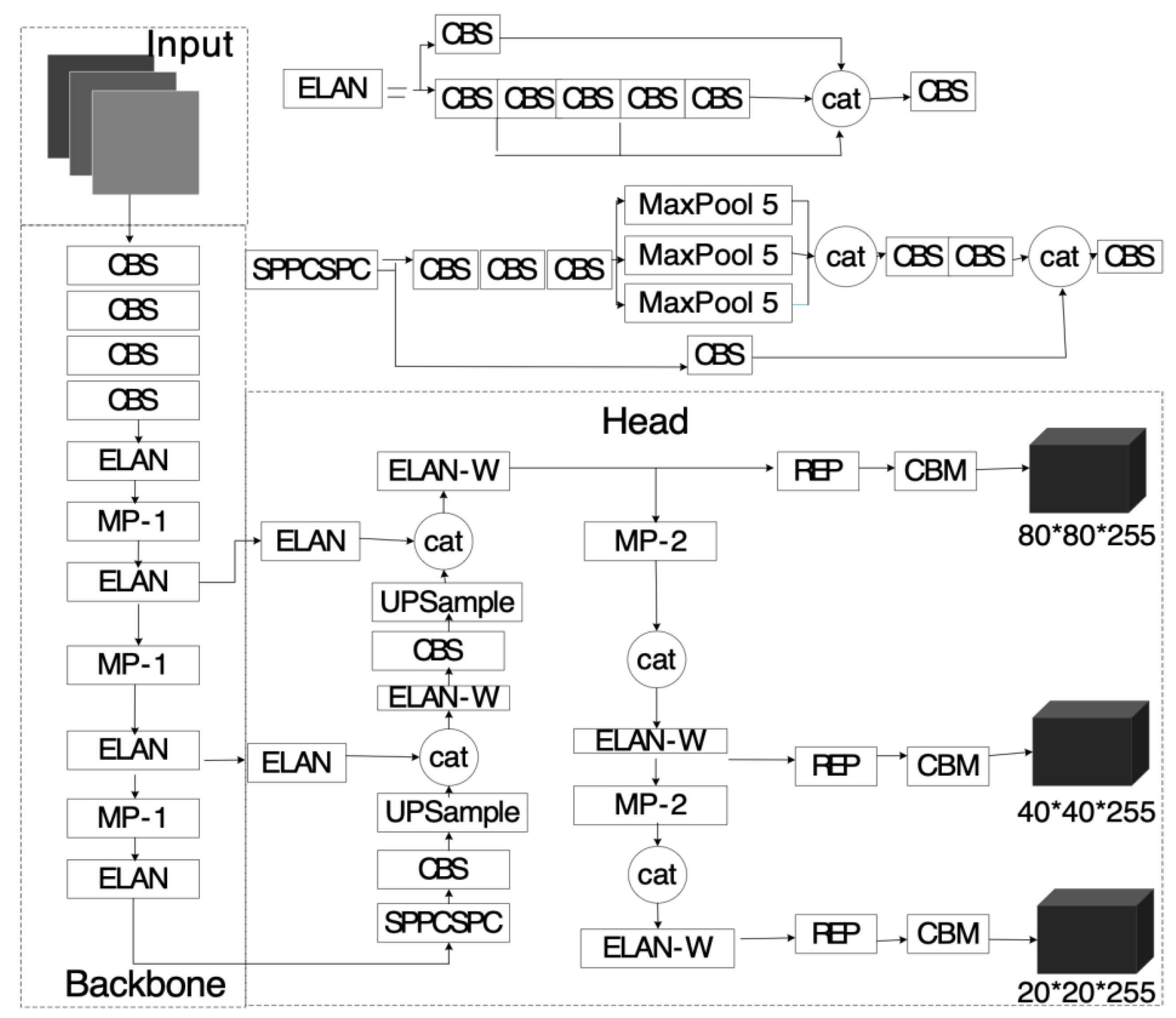
3.1. YOLOv7 Description

The YOLOv7 algorithm is a one-phase target detector that excels in both speed and accuracy within the 5 FPS to 160 FPS range. Its main contributions include model reparameterization, which is introduced into the network architecture, a label allocation strategy that adopts cross-grid search and matching, and an efficient network architecture proposed by ELAN. The algorithm also includes a training method of auxiliary head that aims to increase the training cost and enhance accuracy without affecting the reasoning time, as the auxiliary head only appears in the training process. The YOLOv7 network comprises three parts, and the specific structure is illustrated in Figure 1.
Input: To prepare input images for the network, several preprocessing steps are performed. These steps include random scaling, cropping, and splicing to enrich the dataset and add small targets to make the network more robust. The best anchor is adaptively calculated from the training sets. The images are then uniformly scaled to a standard size and input to the backbone network.
Backbone: This module is extensively utilized for feature extraction and comprises CBS, ELAN, and MP-1 structures. CBS, which is composed of Conv + BN + SiLU, is primarily employed for image channel alteration, feature extraction, and image downsampling. ELAN enhances network robustness by extracting additional features and controlling the shortest and longest gradient paths. ELAN comprises two branches, with the first branch passing through a 1 × 1 convolution module and the second branch through four 3 × 3 convolution modules to extract features, then the four features are merged to obtain the final feature extraction result. Based on ELAN design, E-ELAN employs merge cardinality, shuffle, and expand techniques to enhance network learning capacity while preserving the initial gradient path. MP involves two branches, max pooling and Conv with stride = 2, that are used simultaneously for image downsampling, and the number of channels before and after remains constant.
Head: The backbone network persists in producing three-layer feature maps with varying sizes. The RepVGG block and Conv are followed by the prediction of three image detection tasks: classification, background classification, and frame. Auxiliary head training and positive and negative sample matching strategies are employed to enhance the overall performance of the model.

3.2. Improved Swin Transformer v2

3.2.1. Swin Transformer v2

Deep learning networks often encounter challenges during training and application, such as (1) visual models being prone to large-scale instability; (2) high-resolution images or windows being required for many downstream visual tasks; and (3) high graphics processing unit (GPU) memory consumption when dealing with large images and high resolutions. To tackle these issues, Liu et al. proposed the Swin Transformer technology [11], which includes (1) post-normalization technology and scaling cosine attention to enhance the stability of large visual tasks; and (2) a log-spaced continuous location deviation method to enable the model trained on coarse images to be applied to higher-resolution counterparts. The specific structure is depicted in Figure 2. Furthermore, zero redundancy optimizers, activation checkpoints, and sequential self-attention calculations can significantly reduce GPU memory consumption. By training a Swin Transformer model using these methods, it can be applied to large visual tasks, including those involving high-resolution images, while mitigating model instability and GPU memory consumption. The structure of Swin Transformer v2 is shown in Figure 2.
The structure of the Swin Transformer Block is shown in Figure 3.
The reason for the instability in the training process is the difference in amplitude of the interlayer activation function, caused by adding a chief branch between the output of left elements. To address this issue, the Swin Transformer V2 relocates the LN layer. Specifically, for the maximum model training (Swin V2-H and Swin V2-G), an additional LN layer is added to every six Transformer modules to ensure training stability. While the attention of pixel pairs is typically computed by taking the dot product of key vectors, this method often leads to several pixel pairs controlling the attention graph for a number of blocks and heads. To mitigate this problem, a scaling cosine attention method is proposed that calculates the attention of pixel i and pixel j by scaling cosine.
S i m q i , K j = c o s q i , K j / π + B i j
In this context, the variable π is a parameter that can be learned and is not shared across layers or sets of layers. Typically, it has a value greater than 0.01 and represents the difference in relative position between pixel i and pixel j. The cosine function, due to its natural normalization, results in low attention values. Rather than directly optimizing the deviation parameters, the continuous relative position deviation method employs a small element network in the relative coordinates:
B x , y = g x , y
The symbol g in this equation represents a small meta-network consisting of two layers of multi-layer perceptron (MLP) and a ReLU activation function. x , y corresponds to the scaled coordinate of linear space, and the new deviation is learned from the original deviation. If the training is parameterized directly and the pre-trained bias parameters are not used, then the performance of the window may suffer when it is promoted to high resolution. The network g generates a deviation value for any relative position, which makes it suitable for fine-tuning tasks with randomly variable window sizes. During the reasoning process, the bias value for each relative position can be calculated in advance and saved as a model parameter. This approach ensures that the initial parameterized bias method and reasoning process remain consistent.
To accommodate significant changes in window size, a significant proportion of relative coordinate ranges would need to be extrapolated. To address this challenge, logarithmic space is used instead of linear space:
x ^ = s i g n x · l o g 1 + | x |
y ^ = s i g n y · l o g 1 + | y |
In this context, ( x ^ , y ^ ) represents the coordinate in logarithmic space. The use of logarithmic interval coordinates results in a significantly reduced extrapolation ratio when passing relative position deviations compared to using the original linear interval coordinates.

3.2.2. SwinV2_TDD

To better capture local information and accurately locate defect areas in PCB defect detection, Swin Transformer v2 has been improved. As defects tend to be concentrated in local areas, greater attention is required for local information. The first improvement involves adding a convolutional layer with a 3 × 3 kernel to the head of each stage of Swin Transformer v2. Additionally, a pooling operation with a 2 × 2 max pooling operation is added to each stage’s convolutional layer to reduce the size of feature maps and improve the computation efficiency. This results in faster feature extraction while maintaining high-quality feature extraction and reducing memory consumption.
To prevent excessive compression of feature maps and enhance the feature’s expressive power, an upsampling layer with a 2 × 2 upsampling operation is added after each stage’s convolutional layer to restore the feature map to its original size. This ensures that the feature maps are not excessively compressed, thus, improving expressive power. The improved Swin Transformer v2 structure is illustrated in Figure 4, and this enhanced model is referred to as SwinV2_TDD.

3.3. Improved SA Mechanism

3.3.1. SA

The SA module is a neural network module that processes input features and aims to enhance the performance of convolutional neural networks by establishing relationships between features in both the spatial and channel dimensions. It leverages channel splitting and Shuffle units to integrate channel and spatial attention into each group block for processing input features. The input features of the SA module are a four-dimensional tensor with a shape of [N, C, H, W], where N represents the batch size, C represents the number of channels, and H and W represent the height and width of the input image, respectively. The SA module divides the input feature map into multiple groups and incorporates channel and spatial attention into a block of each group using the Shuffle unit. This reduces the dependence between features and improves computational efficiency through parallel computing.
The channel attention branch of SA utilizes global average pooling (GAP) to generate channel-wise statistics, followed by scaling and shifting the channel vector using a pair of parameters. More specifically, for each subgroup of features, a C-dimensional vector is produced using global average pooling, representing the average value of all channels in that subgroup. Then, an MLP is applied to this vector, resulting in scaling and shifting parameters utilized to scale and shift each channel in the subgroup.
The spatial attention branch generates a tensor of shape H × W × 1 using group normalization, representing the sum of squares of channel values at each spatial position. Then, an MLP is used to process this tensor, generating scaling and shifting parameters applied to each pixel in the subgroup. Finally, the outputs of the spatial and channel attention branches are added together and normalized using batch normalization.
The Shuffle unit is a component in the SA module that swaps channels to reduce coupling between features and improve computational efficiency. It splits the input tensor into two parts, one that requires channel swapping and the other that does not. The sub-tensor channels that need swapping are interleaved and concatenated to achieve channel swapping, increasing data diversity and improving generalization ability while reducing the risk of overfitting.
The SA module then combines the outputs of the channel attention and spatial attention branches, which are normalized with a normalization layer to avoid gradient problems, such as vanishing or exploding gradients, and facilitate better feature learning. The SA process and structure are illustrated in Figure 5.
The SA module applies “channel segmentation” to process sets of sub-features in parallel, dividing the input feature map into groups and integrating channel attention and spatial attention within each group using the Shuffle unit. In the channel attention branch, global average pooling is utilized to create channel-wise statistics, which are then scaled and shifted by a pair of parameters. In the spatial attention branch, spatial statistics are generated using group normalization, then scaled and shifted to create compact features similar to the channel information. The two branches are combined, and the Shuffle unit is used for each sub-feature to capture feature dependencies in both spatial and channel dimensions. Finally, the sub-features are merged using the “channel shuffle” operator to enable message communication among each sub-feature.

3.3.2. MFSA

In YOLOv7, when the input image size is (640, 640), the model produces three prediction layers of varying sizes, specifically (20, 20), (40, 40), and (80, 80). However, as PCB defects are typically small in size and there are relatively fewer large targets, it is important to focus on improving the recognition accuracy of smaller objects [39]. To achieve this, the paper proposes using the SA mechanism module, which applies weights to different scale prediction layers to highlight the proportion of small-scale targets. This attention mechanism has improved the accuracy of recognizing low-contrast objects in the model.
The SA module is effective at capturing features of different scales and orientations in images by combining interactions between channels and spatial dimensions. However, the attention calculation in SA is limited by the use of a simple, fully connected layer, which may lead to problems such as gradient vanishing. To address this issue, a 1 × 1 convolution layer is added to increase the depth and enhance the adaptive nature of the attention mechanism, allowing the network to better adapt to different tasks and datasets. Additionally, a magnification factor is introduced to dynamically adjust the model’s perception of data, which improves its nonlinear fitting ability and overall accuracy. The optimal value of the magnification factor can be determined through experimentation.
The MFSA mechanism depicted in Figure 6 is achieved by adding a shortcut connection and applying a max pooling layer. The input data is processed, and each channel is multiplied to produce a feature map that completes the original feature relocation of the channel dimension data, resulting in enhanced model performance.
The original computation of SA is expressed as follows:
f c = 1 N i = 1 N α i x i W c , i
where x i represents the i-th feature map in the input tensor, N represents the number of channels in the input tensor, α i represents the attention weights, and W c , i represents the weights after channel shuffling. After adding convolutional layers and a scaling factor s, the above computation can be expressed as the following formula:
f c = 1 N i = 1 N α i x i ( W c , i + W c , j ) s
where W c , j represents the weights after the convolutional operation, and s represents the scaling factor.

3.4. Change the Activation Function to Mish

Activation functions are crucial components in deep learning, enabling complex neural network architectures, and improving learning ability. In recent years, the Swish activation function has emerged as a dominant player in the field. This function is a sigmoid-weighted linear unit that is smooth, non-monotonic, and has no upper or lower limits. Its computational formula is given below.
f x = x × σ β x
Here, σ x is the sigmoid function:
σ x = 1 1 + e x
β is a trainable parameter. When β = 1, the Swish activation function becomes the SiLU activation function. The YOLOv7 trunk network uses the SiLU [40] activation function in its convolutional layer to avoid the problem of gradient disappearance caused by the saturation of the Sigmoid function. As x is very large, f x approaches x, but when x approximates negative infinity, f x approximates 0. The Mish activation function combines the nonlinear characteristics of both tanh and sigmoid functions, and exhibits stronger nonlinear expression ability when the input value is small. The defects on the PCB are relatively small and require precise extraction and processing of details and edge information during detection. The Mish activation function can better capture the detailed information in the image and improve the accuracy of object detection. At the same time, the derivative of the Mish activation function has a shape similar to that of a function with an adaptive slope, which can alleviate the problem of gradient disappearance and improve the training stability and convergence speed of the model. Therefore, the Mish function [41] was used to replace SiLU. The Mish computational formula is as follows:
f x = x t a n h l n 1 + e x
The Mish activation function is unsaturated [42] and has no upper bound, which helps to avoid the problems of gradient disappearance or explosion caused by saturation, resulting in significantly improved training speeds. Additionally, it has a small weight and a lower bound on the negative axis, which helps to prevent the neuron necrosis phenomenon associated with the ReLU function and produces a strong regularization effect. The function is nearly smooth at every point, making it easier to optimize and more generalizable, and it facilitates the flow of information in deeper networks. The Mish activation function is widely used in YOLOv4 [43], demonstrating a 0.494% improvement over Swish and a 1.671% improvement over ReLU. Figure 7 illustrates the graph of the Mish function.

3.5. Enhanced YOLOv7 Backbone

Based on the characteristics of SwinV2_TDD and MFSA, two ELAN modules in the backbone network of YOLOv7 are replaced with SwinV2_TDD modules, combining the strong modeling capability of the transformer structure with important visual signal priors. Meanwhile, the MFSA mechanism is introduced to enhance the extraction of small-scale features in the image. The original backbone and enhanced backbone structures are shown in Figure 8.

4. Results

4.1. Experimental Conditions
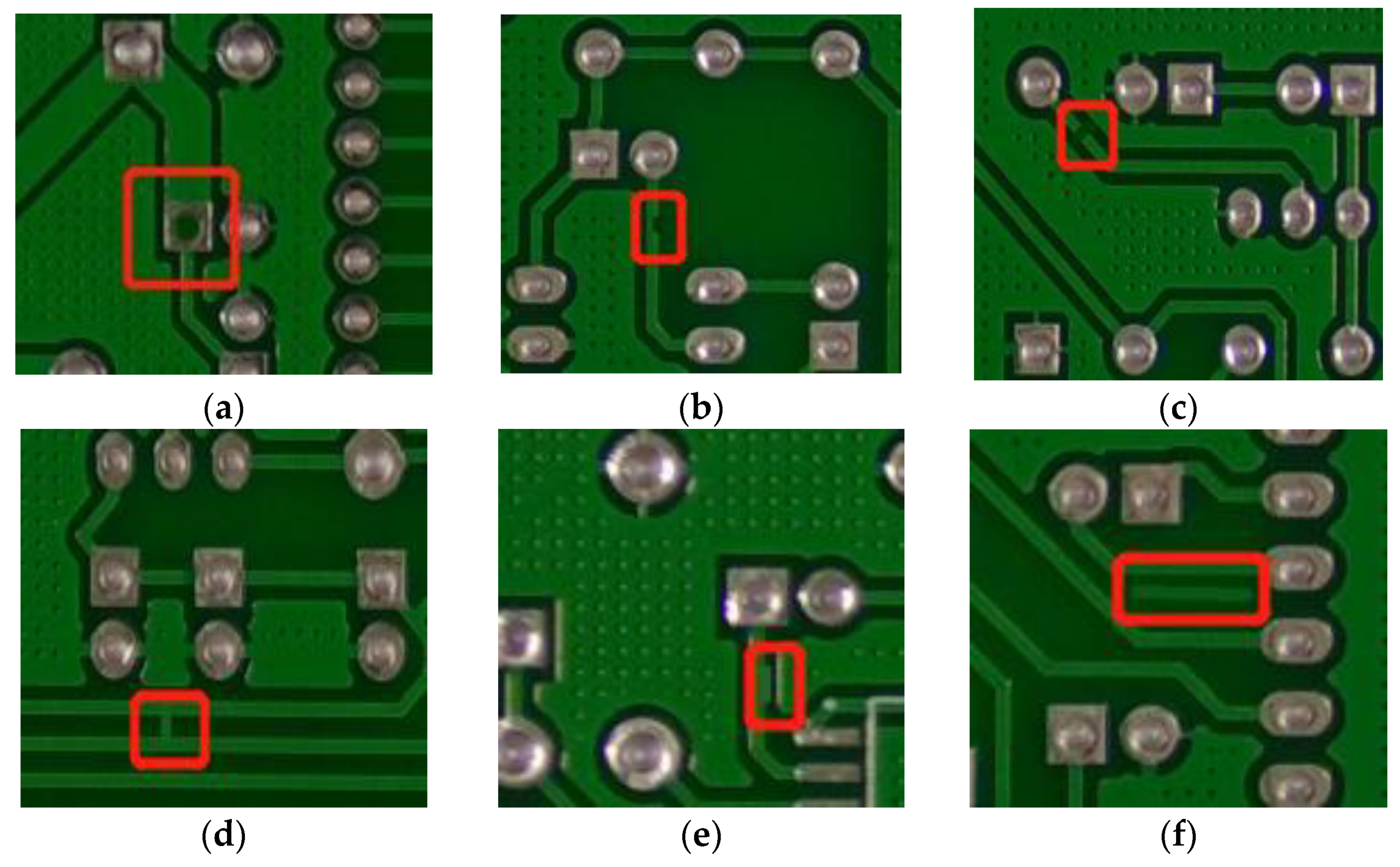
This paper’s experimental environment is based on the Ubuntu 20.04 LTS operating system. The CPU used is AMD Ryzen 7 5800H, and the GPU used is NVIDIA GeForce RTX 3060. The CUDA 11.7 acceleration library is used, and the PyTorch framework is used for implementation.

4.2. Dataset

In this paper, the Intelligent Robot Open Laboratory of Peking University’s open-source dataset [34] is utilized, which includes six types of common defects: missing hole, mouse bite, open circuit, short circuit, spur, and spurious copper, as shown in Figure 9. The dataset comprises a total of 693 images, each containing 3 to 5 defects. The image size is 600 × 600.
The limited size of the dataset used in this study can affect the detection of PCB board defects. To address this, data augmentation techniques were employed to improve the generalization ability of the network during training. Data augmentation is a technique that involves transforming original images through operations, such as rotations, cropping, and scaling, to generate more training data [44]. During model testing, an unaugmented test dataset was used to evaluate the model’s performance and generalization ability. Using the same augmented images for testing as for training can lead to overly optimistic evaluations of the model’s performance because the training and test sets contain different versions of the same original images. To address this issue, the dataset of 693 original images was randomly divided into training and testing sets at an 8:2 ratio. Data augmentation was only applied to the training set, and all images were resized to a uniform size of 640 × 640. The augmented training set contained 9920 images, while the test set contained 139 images, which were original images that had not undergone any augmentation.

4.3. Evaluation Indicators

Precision (P), Recall (R), False Positive Rate (FPR), and mean Average Precision (mAP) were used as evaluation indicators. The ratio between positive samples quantity and all detected samples quantity of this type is denoted as P, and its calculation formula is as follows:
P = T P T P + F P
The ratio between detected positive classes quantity and all positive classes quantity is denoted as R:
R = T P T P + F N
F P R = F P F P + T N
where T P represents the quantity of samples denoted as positive and are actually positive; F P represents the quantity of samples denoted as positive but are actually negative; T N represents the quantity of samples denoted as negative and are actually negative; and F N represents the quantity of samples denoted as negative but are actually positive.
The value of P or R alone cannot objectively reflect the quality of the detection results. Therefore, it is required to combine these two evaluation indexes to measure the performance of the algorithm. Using a combination of points with different P and R values can draw a P-R curve, also called a P-R curve. Based on a P-R curve, AP could be obtained by counting the P value corresponding to each R value. Its computational formula is as follows:
A P = 0 1 P R d R
The sum of all AP classes divided by the number of classes is the mAP:
m A P = i = 0 n A P i n

4.4. Analysis of Experimental Results

4.4.1. Performance Analysis of SwinV2_TDD Structure

In this experiment, we investigated the impact of the SwinV2_TDD structure on model performance. We conducted comparative experiments that included the original YOLOv7 network, the YOLOv7 network with Swin Transformer v2 structure, and the improved YOLOv7 network with SwinV2_TDD structure. To evaluate the performance, we used P, R, and mAP as the metrics. The results of the experiments are presented in Table 1.
Table 1 represents the effectiveness of the proposed SwinV2_TDD method in this paper.
(1) The results indicate that replacing some ELAN modules with the Swin Transformer v2 structure in the original YOLOv7 network improves the P value by 2.56%, R value by 1.66%, and mAP value by 2.06%. This suggests that incorporating the Swin Transformer v2 structure in YOLOv7 can enhance the accuracy of detecting PCB defects.
(2) Moreover, replacing some ELAN modules with the SwinV2_TDD structure in the YOLOv7 network results in a greater improvement in P value by 3.74%, R value by 1.90%, and mAP value by 2.46%, compared to the original YOLOv7 network. Furthermore, compared to adding the Swin Transformer v2 structure to YOLOv7, SwinV2_TDD achieves better P improvement by 1.18%, R improvement by 1.66%, and mAP improvement by 2.06%. Therefore, these findings verify the effectiveness of SwinV2_TDD in achieving higher detection accuracy than Swin Transformer v2 in YOLOv7.

4.4.2. MFSA Magnification Factor Experiment

This experiment aimed to examine how the scaling factor in the MFSA mechanism affects algorithm performance. The study kept other network structures constant and varied the scaling factor to identify the optimal value, ultimately enhancing the model’s performance. mAP and FPR served as the evaluation criteria, and Table 2 shows the comparative results of the experiments.
Based on the findings in Table 2, it is apparent that the mAP of the model improves as the scaling factor increases, whereas the false alarm rate decreases. Specifically, the highest accuracy of the MFSA-YOLOv7 model was achieved at a scaling factor of 3, with a maximum accuracy of 97.16%, and a minimum false alarm rate of 4.21%. However, when the scaling factor exceeds 3, the model’s accuracy starts to decrease while the false alarm rate continues to increase. Thus, the experiment suggests that the optimal value for the scaling factor is 3, since a larger value causes the attention mechanism to learn too much irrelevant information, leading to a decrease in the model’s performance.

4.4.3. Performance Analysis of MFSA Mechanism

The focus of this experiment was to investigate the impact of the improved MFSA mechanism on model performance. The comparative study comprised three models: the original YOLOv7 network, the YOLOv7 network with the SA mechanism, and the YOLOv7 network with the improved MFSA mechanism, which utilized a scaling factor of 3. P, R, and mAP were the evaluation metrics used, and Table 3 presents the experimental results.
Table 3 shows the effectiveness of the proposed MFSA mechanism in this paper. The following observations can be made.
(1) When compared to the original YOLOv7 network, introducing the SA mechanism in the YOLOv7 network resulted in an increased P value by 2.16%, R value by 1.00%, and mAP value by 1.46% in detecting PCB defects. This suggests that incorporating the SA mechanism in the YOLOv7 network can improve the accuracy of PCB defect detection.
(2) Comparing the original YOLOv7 network to the YOLOv7 network with the MFSA mechanism, it was found that the latter improved the P value by 3.41%, R value by 1.63%, and mAP value by 2.08%. Additionally, when compared to the YOLOv7 network with the SA mechanism, the MFSA mechanism improved the P value by 1.25%, R value by 0.63%, and the mAP value by 0.62%. These results demonstrate that incorporating the MFSA mechanism in the YOLOv7 network can achieve higher detection accuracy than incorporating the SA mechanism, thereby validating the effectiveness of the MFSA mechanism.

4.4.4. Comparison of Model Performance with Different Activation Functions

The impact of various activation functions on the performance of the YOLOv7 network was investigated in this experiment. Activation functions are known to enhance the model’s nonlinear fitting ability and facilitate the learning of intrinsic correlations within the data, ultimately leading to improved model performance. The experiment involved substituting Sigmoid, Relu, SiLU, and Mish activation functions for those in the original YOLOv7 network structure while keeping the network structure unchanged. P, R, and mAP were employed as performance evaluation criteria, and the findings are tabulated in Table 4.
Based on the experiment’s outcomes, the Mish activation function exhibited the best performance, achieving P, R, and mAP scores of 87.93%, 98.34%, and 96.17%, respectively. Compared to the use of the SiLU activation function in the original YOLOv7 network, it outperformed by 1.46%, 1.13%, and 1.09%, correspondingly. Furthermore, compared to Sigmoid and ReLU activation functions, the Mish activation function showed significant improvements in P, R, and mAP. These findings demonstrate that the Mish activation function enhances the model’s nonlinear fitting ability and has a stronger nonlinear expression ability when detecting smaller objects.

4.4.5. Comparison of Performance between Different Models

The results of the PCB defect detection model based on the improved YOLOv7 designed in this work were compared with the current mainstream object detection networks, including SSD512, YOLOv3, YOLOv5, YOLOv7, Faster R-CNN, and DenseNet. The detection results are shown in Table 5.
(1) The experimental results show that the enhanced YOLOv7 network model exhibited the highest accuracy in detecting PCB defects, with P, R, and mAP scores of 94.53%, 99.49%, and 98.74%, respectively. Compared to the original YOLOv7 network, there was a significant improvement of 7.32%, 1.68%, and 3.66% in P, R, and mAP, respectively. Additionally, the improved model also demonstrated notable performance enhancements in comparison to various other popular object detection networks.
(2) Furthermore, the improved YOLOv7 network model achieved its highest mAP0.5:0.95, reaching 53.52%, which is a 2.27% increase compared to the original YOLOv7 network and is also higher than the values achieved by other mainstream object detection networks. These results suggest that based on the improved YOLOv7 network, the enhanced method can maintain high P and R values across different IoU thresholds in PCB defect detection. Therefore, the findings suggest that the accuracy of PCB defect detection can be effectively improved using the enhanced method.

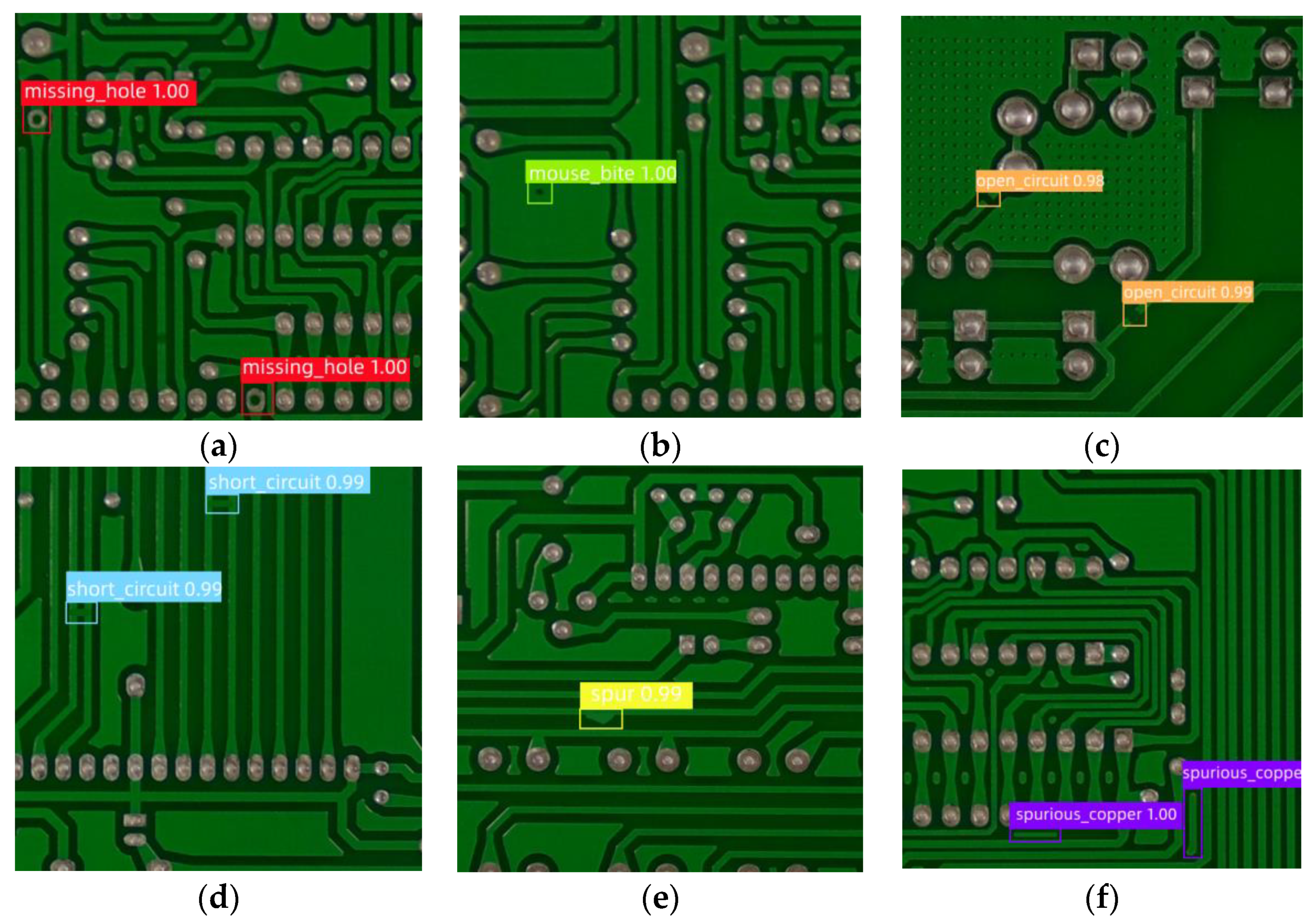
4.4.6. Display of Detection Effect

In the following examples, the enhanced method was able to detect all six types of errors with high accuracy. Specifically, the detection accuracy for missing_hole, mouse_bite, and spurious_copper was 1.00, while the detection accuracy for open_circuit, short_circuit, and spur was 0.99. Figure 10 shows the specific detection effect pictures.

5. Conclusions

The paper presents an improved method for detecting defects in printed circuit boards (PCBs) by enhancing the YOLOv7 network with an improved Swin Transformer V2 structure. The proposed method introduces the MFSA mechanism, which includes a convolutional layer and a scaling factor to enhance the attention mechanism’s adaptability and perception ability. Moreover, the activation function is changed to Mish to increase accuracy and generalization ability. The experiments are conducted on public datasets and a dataset of painted and wired Rigid PCBs. Moreover, the proposed defect detection method is trained and tested only on a dataset of painted and wired rigid PCBs. The results show that the proposed method achieves a higher mAP of 3.66% compared to the original YOLOv7 network, demonstrating its effectiveness for PCB defect detection. However, since detecting small PCB defects is challenging, the network will be further optimized in the future to improve detection accuracy.

Author Contributions

Conceptualization, Y.Y. and H.K.; methodology, Y.Y.; software, Y.Y.; validation, Y.Y. and H.K.; formal analysis, Y.Y.; investigation, Y.Y.; resources, Y.Y.; data curation, Y.Y.; writing—original draft preparation, Y.Y.; writing—review and editing, H.K.; visualization, Y.Y.; supervision, H.K. All authors have read and agreed to the published version of the manuscript.

Funding

This research was funded by the Humanities and Social Sciences research project of the Ministry of Education (grant number 20YJAZH046) and the Scientific Research Project of the Beijing Educational Committee (grant number KM202011232022).

Data Availability Statement

The data that support the findings of this study are available from the corresponding author upon reasonable request.

Acknowledgments

This work was supported by the Humanities and Social Sciences Research Project of the Ministry of Education, the Scientific Research Project of the Beijing Educational Committee, and the Department of Information Security of Beijing Information Science and Technology University.

Conflicts of Interest

The authors declare that they have no competing interest.

References

  1. Zheng, L.J.; Zhang, X.; Wang, C.Y.; Wang, L.F.; Li, S.; Song, Y.X.; Zhang, L.Q. Experimental study of micro-holes position accuracy on drilling flexible printed circuit board. In Proceedings of the 11th Global Conference on Sustainable Manufacturing, Berlin, Germany, 23–25 September 2013. [Google Scholar]
  2. Deng, L. Research on PCB Surface Assembly Defect Detection Method Based on Machine Vision. Master’s Thesis, Wuhan University of Technology, Wuhan, China, 2019. [Google Scholar]
  3. Zhu, Y.; Ling, Z.G.; Zhang, Y.Q. Research progress and prospect of machine vision technology. J. Graph. 2020, 41, 871–890. [Google Scholar]
  4. Khalid, N.K.; Ibrahim, Z.; Abidin, M.S.Z. An Algorithm to Group Defects on Printed Circuit Board for Automated Visual Inspection. Int. J. Simul. Syst. Sci. Technol. 2008, 9, 1–10. [Google Scholar]
  5. Liu, W.; Anguelov, D.; Erhan, D.; Szegedy, C.; Reed, S.; Fu, C.-Y.; Berg, A.C. SSD: Single shot multibox detector. In Proceedings of the Computer Vision–ECCV 2016: 14th European Conference, Amsterdam, The Netherlands, 11–14 October 2016; Part I 14; Springer International Publishing: Berlin/Heidelberg, Germany, 2016; pp. 21–37. [Google Scholar]
  6. Redmon, J.; Divvala, S.; Girshick, R.; Farhadi, A. You only look once: Unified, real-time object detection. In Proceedings of the IEEE Conference on Computer Vision and Pattern Recognition, Las Vegas, NV, USA, 27–30 June 2016; pp. 779–788. [Google Scholar]
  7. Girshick, R.; Donahue, J.; Darrell, T.; Malik, J. Rich feature hierarchies for accurate object detection and semantic segmentation. In Proceedings of the IEEE Conference on Computer Vision and Pattern Recognition, Columbus, OH, USA, 23–28 June 2014; pp. 580–587. [Google Scholar]
  8. Girshick, R. Fast r-cnn. In Proceedings of the IEEE International Conference on Computer Vision, Santiago, Chile, 13–16 December 2015; pp. 1440–1448. [Google Scholar]
  9. Ren, S.; He, K.; Girshick, R.; Sun, J. Faster R-CNN: Towards real-time object detection with region proposal networks. Adv. Neural Inf. Process. Syst. 2015, 28. [Google Scholar] [CrossRef]
  10. Wang, C.Y.; Bochkovskiy, A.; Liao, H.Y.M. YOLOv7: Trainable bag-of-freebies sets new state-of-the-art for real-time object detectors. arXiv 2022, arXiv:2207.02696. [Google Scholar]
  11. Liu, Z.; Hu, H.; Lin, Y.; Yao, Z.; Xie, Z.; Wei, Y.; Ning, J.; Cao, Y.; Zhang, Z.; Dong, L.; et al. Swin transformer v2: Scaling up capacity and resolution. In Proceedings of the IEEE/CVF Conference on Computer Vision and Pattern Recognition, New Orleans, LA, USA, 18–24 June 2022; pp. 12009–12019. [Google Scholar]
  12. Zhang, Q.L.; Yang, Y.B. Sa-net: Shuffle attention for deep convolutional neural networks. In Proceedings of the ICASSP 2021-2021 IEEE International Conference on Acoustics, Speech and Signal Processing (ICASSP), Toronto, ON, Canada, 6–11 June 2021; pp. 2235–2239. [Google Scholar]
  13. Liu, Z.; Qu, B. Machine vision based online detection of PCB defect. Microprocess. Microsyst. 2021, 82, 103807. [Google Scholar] [CrossRef]
  14. Kim, J.; Ko, J.; Choi, H.; Kim, H. Printed circuit board defect detection using deep learning via a skip-connected convolutional autoencoder. Sensors 2021, 21, 4968. [Google Scholar] [CrossRef]
  15. Gaidhane, V.H.; Hote, Y.V.; Singh, V. An efficient similarity measure approach for PCB surface defect detection. Pattern Anal. Appl. 2018, 21, 277–289. [Google Scholar] [CrossRef]
  16. Annaby, M.H.; Fouda, Y.M.; Rushdi, M.A. Improved normalized cross-correlation for defect detection in printed-circuit boards. IEEE Trans. Semicond. Manuf. 2019, 32, 199–211. [Google Scholar] [CrossRef]
  17. Tsai, D.M.; Huang, C.K. Defect detection in electronic surfaces using template-based Fourier image reconstruction. IEEE Trans. Compon. Packag. Manuf. Technol. 2018, 9, 163–172. [Google Scholar] [CrossRef]
  18. Cho, J.W.; Seo, Y.C.; Jung, S.H.; Jung, H.K.; Kim, S.H. A study on real-time defect detection using ultrasound excited thermography. J. Korean Soc. Nondestruct. Test. 2006, 26, 211–219. [Google Scholar]
  19. Dong, J.Y.; Lu, W.T.; Bao, X.M.; Luo, S.Y.; Wang, C.Q.; Xu, W.Q. Research progress of the PCB surface defect detection method based on machine vision. J. Zhejiang Sci.-Tech. Univ. (Nat. Sci. Ed.) 2021, 45, 379–389. [Google Scholar]
  20. Chen, S. Analysis of PCB defect detection technology based on image processing and its importance. Digit. Technol. Appl. 2016, 10, 64–65. [Google Scholar]
  21. Li, Z.M.; Li, H.; Sun, J. Detection of PCB Based on Digital Image Processing. Instrum. Tech. Sens. 2012, 8, 87–89. [Google Scholar]
  22. Liu, B.F.; Li, H.W.; Zhang, S.Y.; Lin, D.X. Automatic Defect Inspection of PCB Bare Board Based on Machine Vision. Ind. Control. Comput. 2014, 27, 7–8. [Google Scholar]
  23. Malge, P.S.; Nadaf, R.S. PCB defect detection, classification and localization using mathematical morphology and image processing tools. Int. J. Comput. Appl. 2014, 87, 40–45. [Google Scholar]
  24. Moganti, M.; Ercal, F. Automatic PCB inspection systems. IEEE Potentials 1995, 14, 6–10. [Google Scholar] [CrossRef]
  25. Ray, S.; Mukherjee, J. A Hybrid Approach for Detection and Classification of the Defects on Printed Circuit Board. Int. J. Comput. Appl. 2015, 121, 42–48. [Google Scholar] [CrossRef]
  26. Ardhy, F.; Hariadi, F.I. Development of SBC based machine-vision system for PCB board assembly automatic optical inspection. In Proceedings of the 2016 International Symposium on Electronics and Smart Devices (ISESD), Bandung, Indonesia, 29–30 November 2016; pp. 386–393. [Google Scholar]
  27. Baygin, M.; Karakose, M.; Sarimaden, A.; Akin, E. Machine vision-based defect detection approach using image processing. In Proceedings of the 2017 International Artificial Intelligence and Data Processing Symposium (IDAP), Malatya, Turkey, 16–17 September 2017; pp. 1–5. [Google Scholar]
  28. Ma, J. Defect detection and recognition of bare PCB based on computer vision. In Proceedings of the 2017 36th Chinese Control Conference (CCC), Dalian, China, 26–28 July 2017; pp. 11023–11028. [Google Scholar]
  29. Deng, Y.S.; Luo, A.C.; Dai, M.J. Building an automatic defect verification system using deep neural network for pcb defect classification. In Proceedings of the 2018 4th International Conference on Frontiers of Signal Processing (ICFSP), Poitiers, France, 24–27 September 2018; pp. 145–149. [Google Scholar]
  30. Huang, G.; Liu, Z.; Van Der Maaten, L.; Weinberger, K.Q. Densely connected convolutional networks. In Proceedings of the IEEE Conference on Computer Vision and Pattern Recognition, Honolulu, HI, USA, 21–26 July 2017; pp. 4700–4708. [Google Scholar]
  31. Huang, W.; Wei, P. A PCB dataset for defects detection and classification. arXiv 2019, arXiv:1901.08204. [Google Scholar]
  32. He, X.Z. Research on Image Detection of Solder Joint Defects Based on Deep Learning. Master’s Thesis, Southwest University of Science and Technology, Mianyang, China, 2021; pp. 30–38. [Google Scholar]
  33. Geng, Z.; Gong, T. PCB surface defect detection based on improved Faster R-CNN. Mod. Comput. 2021, 19, 89–93. [Google Scholar]
  34. Ding, R.; Dai, L.; Li, G.; Liu, H. TDD-net: A tiny defect detection network for printed circuit boards. CAAI Trans. Intell. Technol. 2019, 4, 110–116. [Google Scholar] [CrossRef]
  35. Sun, C.; Deng, X.Y.; Li, Y.; Zhu, J.R. PCB defect detection based on improved Inception-ResNet-v2. Inf. Technol. 2020, 44, 4. [Google Scholar]
  36. Hu, S.S.; Xiao, Y.; Wang, B.S.; Yin, J.Y. Research on PCB defect detection based on deep learning. Electr. Meas. Instrum. 2021, 58, 139–145. [Google Scholar]
  37. Li, C.F.; Cai, J.L.; Qiu, S.H.; Liang, H.J. Defect detection of PCB based on improved YOLOv4 algorithm. Electron. Meas. Technol. 2021, 44, 146–153. [Google Scholar]
  38. Wang, S.Q.; Lu, H.; Lu, D.; Liu, Y.; Yao, R. PCB Board Defect Detection Based on Lightweight Artificial Neural Network. Instrum. Tech. Sens. 2022, 5, 98–104. [Google Scholar]
  39. Zhou, W.J.; Li, F.; Xue, F. Identification of Butterfly Species in the Wild Based on YOLOv3 and Attention Mechanism. J. Zhengzhou Univ. (Eng. Sci.) 2022, 43, 34–40. [Google Scholar] [CrossRef]
  40. Elfwing, S.; Uchibe, E.; Doya, K. Sigmoid-weighted linear units for neural network function approximation in reinforcement learning. Neural Netw. 2018, 107, 3–11. [Google Scholar] [CrossRef]
  41. Misra, D. Mish: A self-regularized non-monotonic activation function. arXiv 2019, arXiv:1908.08681. [Google Scholar]
  42. Kateb, Y.; Meglouli, H.; Khebli, A. Steel surface defect detection using convolutional neural network. Alger. J. Signals Syst. 2020, 5, 203–208. [Google Scholar] [CrossRef]
  43. Guo, X. Research on PCB Bare Board Defect Detection Algorithm Based on Deep Learning. Master’s Thesis, Nanchang University, Nanchang, China, 2021. [Google Scholar] [CrossRef]
  44. Guo, D.; Qiu, B.; Liu, Y.; Xiang, G. Supernova Detection Based on Multi-scale Fusion Faster RCNN. In Proceedings of the 2021 6th International Conference on Intelligent Computing and Signal Processing (ICSP), Xi’an, China, 9–11 April 2021. [Google Scholar]
Figure 1. YOLOv7 Network structure.
Electronics 12 02120 g001
Figure 2. Swin Transformer v2 structure.
Electronics 12 02120 g002
Figure 3. Swin Transformer Block structure.
Electronics 12 02120 g003
Figure 4. SwinV2_TDD structure.
Electronics 12 02120 g004
Figure 5. Shuffle Attention structure.
Electronics 12 02120 g005
Figure 6. MFSA structure.
Electronics 12 02120 g006
Figure 7. Mish function graph.
Electronics 12 02120 g007
Figure 8. Enhanced backbone structure comparison: (left) original backbone and (right) enhanced backbone.
Electronics 12 02120 g008
Figure 9. Diagram of six defect types (a) missing hole; (b) mouse bite; (c) open circuit; (d) short circuit; (e) spur; (f) spurious copper.
Electronics 12 02120 g009
Figure 10. Sample test results: (a) missing hole; (b) mouse bite; (c) open circuit; (d) short circuit; (e) spur; (f) spurious copper.
Electronics 12 02120 g010
Table 1. Analysis and Comparison of SwinV2_TDD Structure Performance.
ExperimentsP/%R/%mAP/%mAP0.5:0.95/%
YOLOv7s86.4797.2195.0851.25
Swin Transformer v2-YOLOv789.0398.8797.1452.47
SwinV2_TDD-YOLOv790.2199.1197.5453.50
Table 2. The influence of different magnification factors on model performance.
Magnification FactormAP/%FPR/%
193.237.64
296.055.22
397.164.41
496.785.60
595.566.85
693.047.02
793.737.19
891.567.78
991.048.56
Table 3. Performance analysis of MFSA mechanism.
ExperimentsP/%R/%mAP/%mAP0.5:0.95/%
YOLOv7s86.4797.2195.0851.25
SA-YOLOv788.6398.2196.5451.92
MFSA-YOLOv789.8898.8497.1652.73
Table 4. Comparison of model performance with different activation functions.
ExperimentsP/%R/%mAP/%mAP0.5:0.95/%
Sigmoid83.6294.1992.3848.61
ReLU85.4196.1294.7850.93
SiLU86.4797.2195.0851.25
Mish87.9398.3496.1751.74
Table 5. Comparison of performances of different models.
AlgorithmsP/%R/%mAP/%mAP0.5:0.95/%
SSD51284.0794.8592.0948.79
YOLOv385.1395.3692.7549.12
YOLOv5s86.4797.2194.6950.53
YOLOv7s87.2197.8195.0851.25
Faster R-CNN85.4296.4893.0849.87
DenseNet87.3597.4694.1251.39
Our proposed94.5399.4998.7453.52
Disclaimer/Publisher’s Note: The statements, opinions and data contained in all publications are solely those of the individual author(s) and contributor(s) and not of MDPI and/or the editor(s). MDPI and/or the editor(s) disclaim responsibility for any injury to people or property resulting from any ideas, methods, instructions or products referred to in the content.

