Article

A Datasheet-Driven Electrothermal Averaged Model of a Diode–MOSFET Switch for Fast Simulations of DC–DC Converters

by
Paweł Górecki
1,2,* and
Vincenzo d’Alessandro
2
1
Department of Marine Electronics, Gdynia Maritime University, Morska 83, 81-225 Gdynia, Poland
2
Department of Electrical Engineering and Information Technology, University Federico II, 80125 Naples, Italy
*
Author to whom correspondence should be addressed.
Electronics 2024, 13(1), 154; https://doi.org/10.3390/electronics13010154
Submission received: 20 November 2023 / Revised: 19 December 2023 / Accepted: 26 December 2023 / Published: 29 December 2023
(This article belongs to the Section Power Electronics)

Abstract

:
The design of modern power electronics converters requires accurate electrothermal device models enabling a straightforward parameter estimation and fast, yet accurate, circuit simulations. In this paper, a novel electrothermal averaged model of a diode–MOSFET switch for fast analysis of DC–DC converters is proposed. The model has the form of a SPICE-compatible subcircuit and allows computing in a very short simulation time the DC characteristics of the converter, the waveforms of the terminal voltages and currents of the semiconductor devices, as well as their junction temperatures, both in CCM and DCM.. All the input data required by the parameter estimation procedure can be taken from the datasheets of components. The correctness of the proposed approach is experimentally verified for a buck converter chosen as a case-study. A generally good agreement between measurements and simulations is obtained; as an example, the absolute error in assessing the MOSFET junction temperature does not exceed 12 °C within the whole range of switching frequency of the converter, while the commonly used PLECS model considerably underestimates it.

1. Introduction

DC–DC converters are used for countless applications including electrical vehicles, industrial automation, medical devices, renewable energy, smartphones, and so on [1]. Among many isolated and non-isolated topologies [2], these converters typically include at least one diode–transistor switch, i.e., the connection of these two devices in which the current alternately flows.
In the design process of power converters, a major role is played by computer simulations [3], which should be fast and as accurate as possible. Typically, in circuit-level simulations of power converters, programs like PLECS [4] (piecewise linear electrical circuit simulation) or SPICE (simulation program with integrated circuits emphasis) are used [3]. Many manufacturers of semiconductor devices offer PLECS- and SPICE-compatible models on their websites.
Factors that strongly influence the accuracy and duration of analysis are the computation method adopted and the complexity level of the model. In PLECS, simple models of semiconductor devices are available, which allow for fast simulations of power converters operating with hundreds or thousands of volts [5]. Moreover, it is possible to perform electrothermal simulations of the converters by computing the temperature of each individual component. However, the accuracy of the simulation outcomes may be poor, since the influence of the junction and ambient temperatures on the thermal resistance of the devices is neglected [6,7]. In addition, the closed structure of this program does not allow for the implementation of solutions known from the literature to solve this problem.
Contrary to PLECS, SPICE is a program with an open structure and numerous free versions. In SPICE, it is possible to implement any mathematical equation using controlled current and voltage sources. Although SPICE libraries do not contain elements conceived for electrothermal analysis, these can be easily accounted for using the thermal equivalent of Ohm’s law [8]. Another relevant SPICE advantage is the accurate mapping of the switching behavior of semiconductor devices, including overcurrents and overvoltages which result from the parasitic properties of the analyzed converter. This is particularly important not only because too-high peaks of either current or voltage may destroy a device, but also because even moderate pulses influence switching energy losses, and consequently the junction temperatures [9].
However, transient simulations of DC–DC converters require a long CPU time in SPICE [10]. An analysis of semiconductor devices placed on heatsinks and operating in natural heat convection conditions may even last some hours, which is unacceptable from an engineer’s perspective: if simulations are part of the design process, the simulation time should not exceed a few minutes.
This problem can be tackled by resorting to methods for fast analysis of power electronic converters recently proposed in literature [11,12,13,14,15,16]. For the case of DC–DC converters, the use of averaged diode–transistor switch models is particularly attractive. Such models allow obtaining the average values of terminal voltages and currents of the devices, as well as their junction temperatures, under steady-state conditions. As a DC analysis needs to be performed, it is possible to significantly shorten the computation time with respect to a conventional transient simulation [10]. Moreover, it is possible to sweep key variables like switching frequency, load resistance, or duty cycle, which allows for an easy assessment of the maximum load current and selection of the switching frequency.
In the literature, numerous models of diode–transistor switches for averaged analyses of DC–DC converters can be found, which include ideal switches [16,17,18], MOSFETs (metal oxide semiconductor field effect transistors) [19,20,21], and IGBTs (insulated gate bipolar transistors) [22,23]. Unfortunately, most of them have some drawbacks. In models using ideal switches, it is assumed that no power is dissipated in the semiconductor devices, and therefore it is not possible to use them to formulate an electrothermal model of the converter in which the temperature is determined from the dissipated power. The cited models of the diode–MOSFET switch suffer from limited accuracy, as they do not take into account numerous phenomena, examples of this being the dependence on the thermal resistance on junction temperature, switching losses, and the influence of overcurrents and overvoltages on them [19,20,21]. In [22], a model of a diode–IGBT switch is presented, which accounts for all the above-mentioned phenomena, although the description of overcurrents and overvoltages is correct only in a narrow range of currents and voltages.
Regardless of the computation method used, each model has parameters whose values must be determined before computation. From an engineer’s point of view, it is desirable to estimate them from the datasheets of the used components, the layout of PCB, and cable project. Models whose parameter values may be estimated using only datasheets are called datasheet-driven models [24]. When datasheet-driven models are employed, it is possible to perform a simulation without physically possessing the components.
All the aforementioned literature solutions have visible drawbacks. None of them accounts for nonlinear thermal effects and switching losses, allows the computing of the peak values of transistor current and voltage, or at the same time enjoys a short simulation time and is associated with a datasheet-driven procedure of parameter estimation.
This paper presents a datasheet-driven SPICE-compatible electrothermal averaged model of a diode–MOSFET switch for fast analysis of DC–DC converters, which accounts for (i) the dependence of the thermal resistance on the junction temperature, (ii) switching losses, (iii) overcurrents and overvoltages occurring when switching devices, and (iv) influence of delay times of the transistor and driver on the duty cycle. Using such a model, it is possible to compute the average values of voltages, currents, and junction temperatures of the semiconductor devices in the converter with higher accuracy than the literature models [4]. Moreover, differently from other averaged models, the proposed model allows computing the waveforms of terminal voltages and currents of the semiconductor devices. All parameters of the model are determined on the basis of the datasheets of the components used, PCB layout, and cable project. The main novelties are: shortened duration of the electrothermal simulations of a power converter for a DC analysis maintaining the possibility of computing waveforms of drain current and drain–source voltage of the transistor in steady-state, and datasheet-driven procedure of parameter estimation.
The article is organized as follows. In Section 2, the model form is presented. Section 3 describes the procedure for parameter estimation of the proposed model. Section 4 provides an accuracy verification of the model based on experimental data, as well as a discussion about its properties. Conclusions are then given in Section 5.
A .cir file for analysis in SPICE is attached to the article as Supplementary Material.

2. Model Form

Figure 1 shows the circuit representation of the model. It consists of 5 parts. The first one is the main circuit, in which the average values of the voltages and currents of transistor (MOSFET) and diode are calculated. The junction temperatures are determined in the thermal model block. The CCM/DCM (continuous conduction mode/discontinuous conduction mode) block is used to evaluate the equivalent duty cycle of the control signal. In the overcurrent and overvoltage block, the VDS voltage increase during switching off and the ID current increase during switching on are determined. The input data needed to perform all computations in the above-mentioned blocks are computed in the auxiliary sources block. It is worth noting that some of equations in this block regarding inductor current depend on the converter topology.
The main circuit is the averaged model of the diode–transistor switch. The terminals of this circuit represent terminals of the two devices: 1 is the MOSFET drain, 2 is the source, 3 is the diode cathode, and 4 is the anode. The other blocks are used to compute input data for the main circuit and keep equations describing output current and voltages of the controlled source in the main circuit as simple as possible. Moreover, data computed in these blocks may be used to draw a simplified waveform of the terminal voltages and currents of the MOSFET and the diode. The main circuit is based on the concept presented in [16,25]. Although the equations describing the efficiency of the sources are only slightly changed, in the proposed approach the overall accuracy is significantly improved thanks to the computations carried out in the other blocks, not included in the literature models in [16,25].

2.1. Main Circuit

The main circuit consists of four sources: ET, ER, GD, and VP. The controlled voltage sources ET and ER are used to model the value of the average voltage between drain and source. The formulas from [25] have been modified to describe the non-linearity of the diode current-voltage characteristics:
E T = 1 E u E u · V 2
E R = R o n a v g · I 1 E u + 1 E u · V D a v g E u
where Eu is the equivalent duty cycle of the control signal accounting for the converter mode of operation and electrical inertia, V1, V2, I1, and I2 are the input and output voltages and currents, VDavg is the average diode voltage during its conduction described as in [22], and Ronavg is the average drain–source on-state MOSFET resistance. The voltage source VP of output value equal to 0 is used to monitor the output current. The controlled-current source GD models the average value of the diode current. The output current of this source is given by [25]:
G D = 1 E u E u · I 1
The value of the Eu coefficient, determined in the CCM/DCM block, in the case of the converter operating in the CCM mode is equal to dreal, which represents the negative duty cycle of the drain–source voltage.

2.2. CCM/DCM Block

As the DC–DC converter operates in DCM, the value of the output voltage is higher than in the case of operation in CCM. The reason for this difference is that the inductor current has dropped to 0 before the end of each DCM cycle. Therefore, in order to correctly model the output voltage of the converter in both modes, the following formula was used [22]:
E u = L I M I T M A X d r e a l , d r e a l 2 d r e a l 2 + 2 · L · f · I 1 V 2 + V D m i n , 0,1
where L is the coil inductance and f the switching frequency. The LIMIT function adopted in (4) is a SPICE standard function that constrains the output value between a lower and an upper limit, while MAX returns the highest of the two arguments [26].
According to the datasheets, the turn-on and turn-off delay times of both the MOSFETs and the related drivers are noticeably different from each other. As a result, the duty cycle of the drain–source voltage decreases with the switching frequency. In order to account for the influence of electrical inertia occurring in both the driver and the MOSFET on the characteristics of the DC–DC converter, the duty cycle is given by:
d r e a l = d + t d o f f t d o n + t d o f f d r i v e r t d o n d r i v e r · f
where d is the duty cycle of the driver input signal, tdoff and tdon are the MOSFET delay times, and tdoffdriver and tdondiver are the driver delay times.
The MOSFET turn-off delay time strongly depends on the gate resistance, and therefore it is computed from:
t d o f f = t d o f f r e f · R G r e f + R G R G r e f

2.3. Thermal Model

The junction temperature of the diode and the MOSFET are computed in the thermal model block, which is directly coupled to the main circuit. The controlled current sources PD and PT model the average values of the powers dissipated in both devices.
As far as the MOSFET is concerned, the dissipated power is computed as:
P T = V D S a v g · I E T + f · E o n + E o f f
where VDSavg is the average value of the drain–source voltage of the turned-on MOSFET, and Eon and Eoff are the turn-on and turn-off switching energy losses, respectively.
The power PD dissipated by the diode is given by:
P D = V D a v g · I 2 + E D · f
where the capacitive energy ED related to reverse recovery in the Schottky diode results only from the parasitic junction capacitance Cj.
The diode and MOSFET are separately described by a thermal model including junction-case thermal resistance Rthj-c, thermal resistance of thermal grease Rthgrease, thermal resistance of ceramic heat transfer pad Rthhtp, and heat-sink thermal resistance Rthhs. The value of the thermal resistance Rthj-c is given in the datasheet for both devices. The thermal resistance of thermal grease is computed from:
R t h g r e a s e = t g r e a s e k g r e a s e · a g r e a s e
where tgrease is the thickness of thermal grease, kgrease is its thermal conductivity, and agrease is the area of the interface. The thermal resistance Rthhtp is computed analogously. The thermal resistance Rthhs is calculated using:
R t h h s = R t h 0 · e x p T h s T 0 T x + R t h 0
which was formulated on the basis of [27]. In (10), Rth0 is the minimal value of heatsink thermal resistance, Ths is the heatsink temperature directly under semiconductor device, and Tx is a parameter characterizing the geometry of heatsink.

2.4. Overcurrents and Overvoltages Block

In the proposed approach, overcurrents and overvoltages occurring while switching power transistors, i.e., the drain current increase during turn-on and drain–source voltage increase during turn-off, are accounted for to assess current and voltage stresses of the devices and accurately compute their influence on switching losses during the design process of the converter.
Iovc is the increase of the current switched on by the transistor resulting from charging the parasitic capacitance of the diode, and is computed using the following equation:
I o v c = Q D t r · r e f 1 r e f 2
where QD is the diode capacitive charge, tr is the rise time, and ref1 and ref2 are the percentage of switched-off drain–source voltage VDC defining the borders in which tr was measured. The charge QD is computed as
Q D = V i n 0 C j d V D = V j · C j 0 m · C j 0 C j 1
where Cj is the diode junction capacitance determined from the classic formula:
C j = C j 0 1 i f v E u > d r e a l ,   V i n · 1 E u , V i n V j m
In (13), Cj0 is the junction capacitance at voltage equal to 0, Vj is the built-in voltage, and m is a coefficient characterizing the type of the junction. The reverse diode voltage at the end of its turn-off phase is computed using the conditional instruction if, because it changes depending on the converter operating mode: in CCM it is equal to Vin, and in DCM it is the product of Vin and the difference between 1 and Eu.
The rise time tr, which is necessary to compute current Iovc, is given by:
t r = d t r 1 · I m i n + d t r 2
where dtr1 and dtr2 are coefficients of the polynomial approximating the datasheet dependence tr(ID).
Vovv is the voltage increase caused by overvoltage computed from:
V o v v = L c a b l e + L t r a c e · I m a x · r e f 1 r e f 2 t f
Lcable and Ltrace being the inductances of cables and trace between input capacitor and diode anode, respectively. If discrete semiconductor devices are used in the design, they can be connected to the rest of the converter via cables or traces. Inductance Lcable is computed using [27]:
L c a b l e = 2 · 10 7 · l c · l n 2 · l c d c · 1 + 1 + d c 2 · l c 2 1 + d c 2 · l c 2 + μ 0 4 + d c 2 · l c
where lc is the sum of cable length between input capacitance and diode anode, dc is the diameter of these cables, and µ0 is the magnetic permeability of vacuum. In turn, the inductance Ltrace between input capacitance and diode anode is given by [27]
L t r a c e = μ 0 · l t · h t + t t 2 w t
where lt is the trace length between input capacitance and anode of the diode, ht is the PCB substrate thickness, wt is the trace width, and tt is the trace thickness.
The fall time is computed as an approximation of the datasheet characteristic according to:
t f = d t f 1 · I m a x + d t f 2 · R G + R G r e f R G r e f
where dtf1 and dtf2 are coefficients of the approximating polynomial.

2.5. Auxiliary Sources

The auxiliary sources are used to compute the parameters used in the other blocks.
The average value of the drain–source on-state resistance Ronavg to be used in (2) is computed by approximation of the datasheet characteristics describing this resistance as a function of the MOSFET junction temperature TjT, the high state of driver output voltage VGShigh, and the conducted drain current ID according to:
R o n a v g = R o n r e f + a R o n · T j T T 0 2 + b R o n · T j T T 0 + a V G S · e x p V G S h i g h b V G S + 1 I L m a x I L m i n I L m i n I L m a x a I D I D 2 + b I D I D d I D = R o n r e f + a R o n · T j T T 0 2 + b R o n · T j T T 0 + a V G S · e x p V G S h i g h b V G S + a I D · I L m a x 2 + I L m i n 2 + I L m a x I L m i n 3 + b I D · I L m a x + I L m i n 2
where Ronref is the drain–source on-state resistance at the reference temperature T0 at ID = 0 and maximum allowable VGS voltage, whereas aRon, bRon, aVGS, bVGS, aID, bID are coefficients of a function approximating the datasheet characteristics Ron(ID,VGS,TjT). aRon, bRon are Ron temperature coefficients, and aVGS and bVGS are used to approximate the influence of VGS on Ron. The current ID of the transistor operating in a DC–DC converter varies in the range defined by the minimum ILmin and maximum ILmax current of the inductor. Therefore, to correctly include the influence of ID in the equation describing Ronavg resistance, polynomial approximation of the Ron(ID) dependence is integrated in this range of currents.
The capacitive energy ED related to reverse recovery in Schottky diodes is used in the computation of temperature TjD. ED is described by approximating the datasheet dependence Cj(VD) according to:
E D = a V D 1 · i f E u > d r e a l , V i n · E u 2 , V i n 2 + a V D 2 · i f E u > d r e a l , V i n · E u , V i n
The voltage switched by the diode changes depending on the converter operating mode: in the CCM mode, the voltage switched by the diode is equal to Vin, and in the DCM mode it is the product of Vin and Eu. aVD1 and aVD2 are the coefficients of the approximating polynomial.
VDSavg is the average value of the drain–source voltage of the turned-on MOSFET used in the evaluation of temperature TjT and is computed as:
V D S a v g = 1 I L m a x I L m i n I L m i n I L m a x I L · R o n d I L = I L m a x + I L m i n 2 · [ R o n r e f + a R o n · T j T T 0 2 + b R o n · T j T T 0 + a V G S · e x p V G S h i g h b V G S ] + a I D I L m a x 3 + I L m a x 2 · I L m i n + I L m a x · I L m i n 2 + I L m i n 3 4 + b I D · I L m a x 2 + I L m i n 2 + I L m a x I L m i n 3
The switching energy losses Eon and Eoff of the MOSFET in (7) are computed by approximation of datasheet characteristics. According to the datasheet, Eon and Eoff are a function of three variables: switched drain current ID, switched voltage VDC, and gate resistance RG. Contrary to IGBT, for a MOSFET, the dependence of switching energy losses on temperature is so weak [28] that it is typically not given by manufacturers in the datasheet. For this reason, it was not included in the formulated model. Compared to the IGBT, the MOSFET dependences of switching energy losses on the switched current and voltage are highly nonlinear, and therefore in the model they are approximated using a 4th-order polynomial. Turn-on switching losses are computed using:
E o n = M A X ( a i o n 1 · I m i n + I o v c 4 + a i o n 2 · I m i n + I o v c 3 + a i o n 3 · I m i n + I o v c 2 + a i o n 4 · I m i n + I o v c · 1 + b v d c o n 1 · V 1 V d c r e f 2 + b v d c o n 2 · V 1 V d c r e f · ( 1 + c R G o n · R G R G r e f ) , 0 )
where aion1, aion2, aion3, aion4, bvdcon1, bvdcon2, cRGon are coefficients of the polynomial, Vdcref and RGref are reference values of switched voltage VDC and resistance RG, for which datasheet characteristics describing switching energy losses are presented.
As in the case of Eon, turn-off energy losses Eoff are determined on the basis of approximation of the datasheet characteristics, using:
E o f f = M A X ( a i o f f 1 · I m a x 2 + a i o f f 2 · I m a x · ( 1 + b v d c o f f 1 · V 1 + V o v v V d c r e f 2 + b v d c o f f 2 · V 1 + V o v v V d c r e f ) · 1 + c R G o f f · R G R G r e f , 0 )
where aioff1, aioff2, bvdcoff1, bvdcoff2, cRGoff are coefficients of the polynomial, and Vovv is voltage increase caused by overvoltage.

3. Estimation of Model Parameters

Using any mathematical model, including the one presented in the paper, requires parameter estimation. Conveniently, the so-called datasheet-driven models require only the parameters and characteristics available in the datasheet. This allows performing simulations before building the real converter. However, the accuracy of the simulations of the converter highly depends on the accuracy and repetitiveness of the input data used in the estimation procedure.
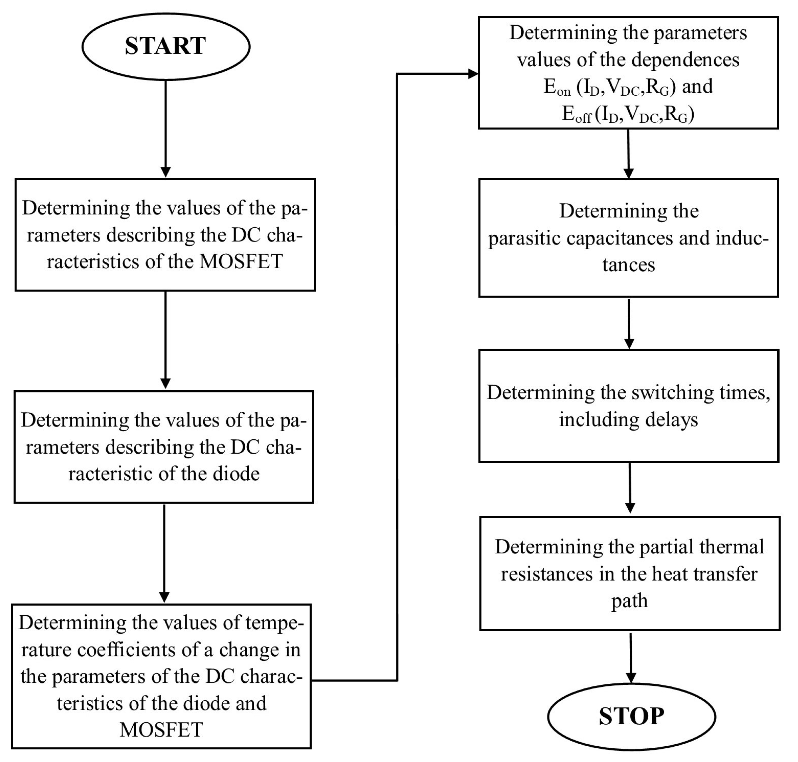
The procedure used to estimate the values of the model parameters is presented in a simplified form in Figure 2, and in detail below.
  • Concerning the output characteristics of the MOSFET, parameters aRon, bRon, aVGS, bVGS, aID, bID are determined approximating the datasheet characteristics Ron(ID, VGS, Tj) of the MOSFET. Ronref in (19) is the value of Ron at the temperature T0 with ID = 0 and the maximum allowable voltage VGS.
  • Concerning the output characteristics of the diode, parameters ISD, nD, and RSD are calibrated using the datasheet current-voltage characteristics of the diode measured at T0. Then, using the datasheet current-voltage characteristics for at least 3 temperatures, parameters KISD and nRSD are estimated.
  • Using the datasheet characteristics Eon(ID, VDC, RG) and Eoff(ID, VDC, RG), the values of parameters aion1, aion2, aion3, aion4, bvdcon1, bvdcon2, cRGon, aioff1, aioff2, bvdcoff1, bvdcoff2, cRGoff in (22) and (23) are determined. These parameters are empirical and should be optimized by adjusting the computed characteristics to match the datasheet ones. VDCref and RGref have the values equal to the reference values of VDC and RG used in the Eoff and Eon characteristics available in the datasheet.
  • Parameters related to the parasitic capacitance of the diode are calibrated on the basis of the datasheet characteristic Cj(VR). In (13), Vj is the built-in voltage determined by adjusting the computed characteristic to the datasheet one, and m is a factor characterizing the type of junction; for an abrupt junction, it is equal to 0.5.
  • The parameters of the equations describe the parasitic inductances resulting from the structure of the circuit are the geometrical parameters of the printed circuit and the cables used.
  • Parameters dtf1, dtf2, dtr1, dtr2 describing the dependence of switching times of the transistor on switched current in (14) and (18) are approximated from the datasheet characteristics tf(ID) and tr(ID).
  • The parameters of the thermal model are estimated using the diode and the MOSFET datasheets, heatsink datasheet, and datasheet of the thermal interfaces between them. Rth0 is typically given by the producer, and Tx is a parameter dependent on heatsink geometry, which is equal to 26 K for a grilled heatsink [29]. kgrease and khtp are given by manufacturers of grease and pads on their packages. In turn, parameters agrease, tgrease, ahtp, and thp are related to the geometry of these interfaces. If measuring the thickness of thermal grease is a cumbersome task, one can use the value given by the manufacturer, or, in the case of its absence, the typical value indicated in the literature, i.e., 100 µm [30].
As results from [31], in some cases, the measured values of parameters of a semiconductor device in real applications visibly differ from the values presented in a datasheet. This may result in a hard-to-assess error in parameter estimation. However, the proposed approach still remains a good option to perform accurate enough simulations at the design stage of the DC–DC converter. A possible alternative is a procedure based on real device measurements, which is free of the above-mentioned error or, for the thermal resistances, an estimation based on FEM simulation [32].
It is worth noting that the values of switching energy losses Eon and Eoff are influenced by parasitic properties of the circuit and components used [33]. In the model, it is assumed that Eon and Eoff used in the estimation procedure were measured in the parasitic-less conditions. Using (11)–(18), the influence of parasitics on switching energy losses is computed and taken into account. If the switching energy losses are based on the measurements of the real converter, using an oscilloscope [31] or calorimetric method [34], parameters Vovv and Iovc should be removed from (22) and (23).
The procedure remains the same regardless of the selected way of preparation of the input data for the estimation of model parameters.

4. Experimental Verification

In order to verify the usefulness of the proposed diode–MOSFET switch model, simulations and measurements of characteristics of a buck converter including such a switch were performed. The experimental analysis was carried out by making use of a discrete 650 V Trench SiC-MOSFET SCT3060AL [35] manufactured by ROHM (Rohm Semiconductor, Kyoto, Japan) and a discrete 650 V SiC-Schottky diode FFSH5065B-F085 [36] fabricated by ON Semiconductor (ON Semiconductor Corporation, Scottsdale, AZ, USA), both packaged in TO-247. During the experimental verification, the semiconductor devices were placed on separate finned heatsinks of dimensions 165 mm × 100 mm × 35 mm. The parameters of the model were estimated using the procedure described in Section 3. As far as the other components are concerned, a choke L1 with inductance of 105 μH, a capacitor C1 with capacity of 330 μF, and three parallel-connected capacitors with capacitance equal to 330 μF labeled in Figure 3 as C2 were used. The control signal of the MOSFET was produced by the function generator Rigol DG1022Z connected to the gate via a resistor RG equal to 22 Ω and a driver IR2125. The junction temperature of semiconductor devices was measured indirectly without removing their caps as [37]:
T j = T c a p + T c a p T a · R t h j c a p R t h j a R t h j c a p
In (24), the cap temperature Tcap was measured using an Optex PT-3S thermometer, the junction–ambient thermal resistance Rthj-a was measured by means of an indirect electrical method using VGS as a thermally sensitive parameter [38], the junction–cap thermal resistance Rthj-cap was measured using an indirect electrical method and the knowledge of the optically measured Tcap under steady-state thermal conditions.
In Figure 3, the circuit diagram for measuring the DC characteristics of the considered converter together with its photo are presented.
The input voltage Vin is provided by a grid-connected autotransformer with full-bridge diode rectifier and a 4.7 mF capacitor filter. A power analyzer Yokogawa WT5000 (Yokogawa Electric Corporation, Tokyo, Japan) was used to measure voltages Vin and Vout and currents Iin and Iout. Measurements of overcurrents and overvoltages were made using an oscilloscope Rigol MSO8104 with voltage probe Pintek DP-25 and current probe Tektronix CPA300. It is worth noting that the finite precision of the instruments can in principle affect the assessment of the accuracy of the proposed model. The used thermometer has measurement accuracy equal to ±3 °C [39], the voltage probe at 1 kV range has resolution equal to 1 V [40], and the current probe accuracy is equal to 1% [41].
Figure 4 shows the circuit representation the buck converter with the main circuit of the proposed model of the diode–MOSFET switch evidenced. As already mentioned in Section 2, the controlled voltage sources ET and ER describe the properties of MOSFET, while the controlled current source GD models the diode. Using such a source configuration, it is possible to obtain the DC characteristics of the buck converter without using sources dedicated to transient analysis. Resistance R1 models traces resistance and resistance resulting from losses in inductor L1 [42].
Using the proposed model in SPICE, no convergence problems were encountered, and the CPU time needed to simulate a single characteristic did not exceed 0.1 s. Conversely, in PLECS, convergence was not always reached, and the CPU time needed to obtain one point of each characteristic was not lower than 3 s.
The values of the electrical and thermal parameters of the formulated model for which the simulation results presented in Figure 5 and Figure 6 were obtained are presented in Table 1. The parameter values were determined through the procedure presented in Section 3.
Figure 5a shows the measured and simulated output characteristics of the constructed converter, while Figure 5b–d report the corresponding dependences: the maximum value of the switched-on current Ipeak, the maximum value of the switched-off voltage Vpeak, and the junction temperature of diode and MOSFET, all as a function of the output current Iout.
As can be seen from Figure 5a, although both the computations performed using the proposed model in SPICE and those carried out with PLECS favorably agree with the experimental data, the proposed model ensures a higher accuracy, as it accounts for the influence of electrical inertia in the transistor and driver on the VDS voltage duty cycle.
However, significant differences occur for the other three characteristics. They originate from the fact that the PLECS model does not include the parasitic capacitances and inductances present in the converter. Conversely, the proposed model implemented in SPICE accurately evaluates both the maximum value of the switched-on current and the switched-off voltage (Figure 5b,c). The absolute error of the proposed model and the measurement data are mainly due to the resolution of the 1 kV voltage probe (1 V). On the other hand, during measurements in DCM mode, the oscillations of the switched voltage had a significant impact on the measured value of the switched-on current occurring when the inductor current is zero [43]. In this case, the maximum value of the switched-on current depends on the oscillating component of the voltage.
The consequence of omitting the overcurrents and overvoltages in the PLECS model is an underestimation of the MOSFET junction temperature (Figure 5d). The use of a linear thermal model also adversely affects the accuracy of computations. More specifically, under the considered operating conditions of the converter, the temperature computed using the PLECS model is even 50 °C lower than the measured value. For the proposed model, the absolute error of simulations does not exceed 12 °C, which is probably caused by the limited accuracy of parameter estimation using datasheet as an input data. Unfortunately, for the considered MOSFET, the thickness of the curve in the Eoff (ID) diagram and the big difference between the scale and presented values could lead to a significant error in the parameter estimation. This dependence is crucial for the accuracy of computations in DCM mode, where turn-off switching losses dominate. Another significant factor reported in the literature [29] influencing the accuracy of both parameter estimation and simulations is the difference between datasheet data and the characteristics of the tested transistor.
Conversely, both models offer a fairly good accuracy in the estimation of the junction temperature of the diode, as their absolute error do not exceed 3 °C.
In Figure 5b,d, the visible discontinuity is caused by the change of the operation mode of the converter.
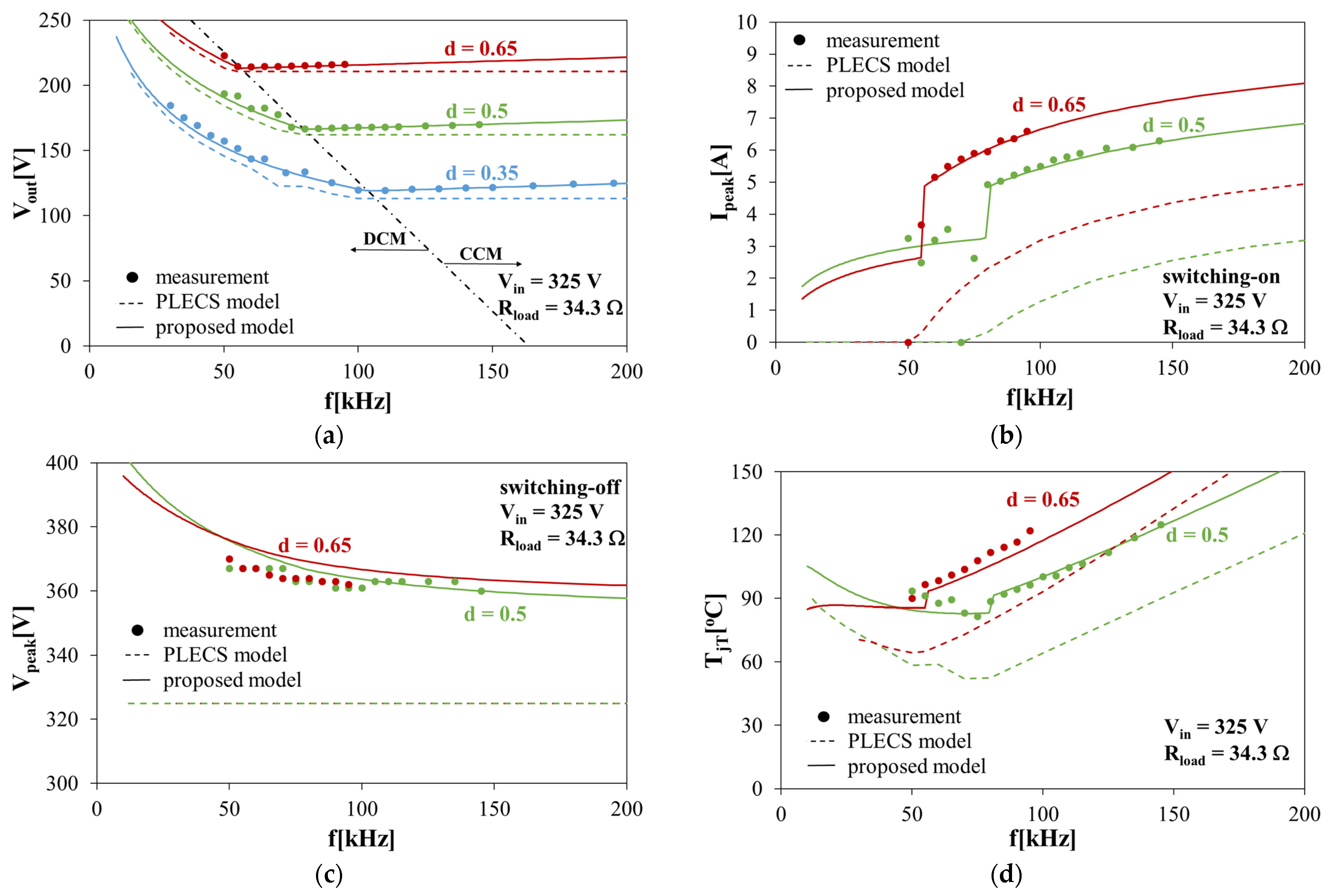
Figure 6a shows the dependence of the output voltage on the switching frequency. Figure 6b–d report the corresponding dependences of the maximum value of the current switched on by the MOSFET (Figure 6b), the voltage switched off by it (Figure 6c), and its junction temperature (Figure 6d) all vs. the switching frequency.
As in the case of the output characteristics of the considered converter, the dependence of the output voltage on the switching frequency is computed with high accuracy in both considered models. However, as can be seen from Figure 6a, the absolute error of PLECS model increases with increasing frequency, as the influence of electrical inertia in the driver and the MOSFET is neglected. As the frequency increases, the influence of inertia causes the difference between the duty cycle of VDS and its value computed using the non-inertia PLECS model. Using the proposed model, high accuracy was obtained in the entire switching frequency range.
Concerning the dependences of the maximum value of the switched-on current (Figure 6b) and the switched-off voltage (Figure 6c) on switching frequency, a high accuracy was obtained only for the proposed model in SPICE. The reason for the high absolute error of the PLECS model is the inability of this software to take into account overcurrents and overvoltages related to transistor switching in the waveforms of the considered converter. Therefore, the voltage and current values computed with the PLECS model are equal to the values for an ideal converter [1]. Consequently, the switching losses and the MOSFET junction temperature computed using PLECS are markedly underestimated. The discrepancies seen in Figure 6d between the computations performed with the proposed model and measurements, visible in the DCM mode similarly as in Figure 5d, are probably caused by the limited accuracy of the parameter estimation procedure from datasheet. Nevertheless, the absolute error in the entire switching frequency range does not exceed 10 °C.
The results presented in Figure 6d can be used to select switching frequency following the method presented in [44]. For the junction temperature selected in the design process, the value of the switching frequency can be directly read from the chart and implemented in the control system, e.g., [45].
Using the proposed approach, it is also possible to obtain the waveforms of the transistor currents and voltages. By exploiting the parameters computed in voltage sources presented in the blocks denoted as “CCM/DCM”, “Overcurrents and overvoltages”, and “Auxiliary sources”, the coordinates of all key points of the waveform may be drawn. The result of such a procedure is presented in Figure 7. In this figure, the results of measurements are identified with lines and the results of simulations with dots.
In Figure 7, the labels describe parameters used to draw the waveform of the VDS voltage and ID current. The time coordinates were calculated from the model parameters f (switching frequency), Eu (equivalent duty cycle), and tf, tr, tdoff, tdon (switching times). It must be remarked that the proposed modeling approach allows computing waveforms under steady state conditions using only 5 points for every waveform. This implies that it is much more effective compared with the traditional approach of transient simulations of DC–DC converters in SPICE, which requires a few thousand points for every period of its operation.
These waveforms may be also computed in PLECS; however, much lower accuracy would be obtained, as in this program overcurrents and overvoltages are not accounted for and switching times are equal to 0.

5. Conclusions

This paper presents a novel approach to electrothermal averaged modeling of a diode–MOSFET switch for the analysis of DC–DC converters. The model formulated using the presented approach allows computing the characteristics of the DC–DC converter in the CCM and DCM modes taking into account electrothermal effects. The advantage of the proposed model over other averaged models known from the literature is the inclusion of the influence on the MOSFET junction temperature of overcurrents and overvoltage occurring during switching. Due to the development of a parameter estimation procedure based solely on datasheet parameters, the model can be easily used by designers of DC–DC converters. Another advantage is the duration of the simulations: each of the characteristics presented in the paper using the proposed model in SPICE takes less than a second on a normal PC.
The usefulness of the proposed modeling approach was confirmed experimentally and by comparison with results obtained with PLECS modeling. The performed verification proved that the formulated averaged model of a diode–MOSFET switch enables a more accurate and faster computation of the MOSFET junction temperature than PLECS simulations. This was possible since the proposed model accounts for the influence of (i) overcurrents and overvoltages on switching energy losses and of (ii) the junction temperature on junction-ambient thermal resistance of the devices. Such effects are both omitted in the PLECS model.

Supplementary Materials

The following supporting information can be downloaded at: https://www.mdpi.com/article/10.3390/electronics13010154/s1, File S1: Elecronics model (1).cir.

Author Contributions

Conceptualization, P.G.; methodology, P.G.; software, P.G.; validation, P.G., V.d.; resources, P.G.; writing—original draft preparation, P.G.; writing—review and editing, P.G. and V.d.; visualization, P.G.; supervision, V.d.; funding acquisition, P.G. All authors have read and agreed to the published version of the manuscript.

Funding

This work was supported by the Polish National Agency for Academic Exchange under grant BPN/BEK/2021/1/00028.

Data Availability Statement

Data is contained within the article or Supplementary Material.

Conflicts of Interest

The authors declare no conflicts of interest.

References

  1. Kazimierczuk, M.K. Pulse-Width Modulated DC-DC Power Converters, 2nd ed.; Wiley: Chichester, UK, 2015. [Google Scholar]
  2. Forouzesh, M.; Siwakoti, Y.P.; Gorji, S.A.; Blaabjerg, F.; Lehman, B. Step-Up DC–DC Converters: A Comprehensive Review of Voltage-Boosting Techniques, Topologies, and Applications. IEEE Trans. Power Electron. 2017, 32, 9143–9178. [Google Scholar] [CrossRef]
  3. Rashid, M.H. Spice for Power Electronics and Electric Power, 1st ed.; CRC Press: Boca Raton, FL, USA, 2006. [Google Scholar]
  4. Allmeling, J.H.; Hammer, W.P. PLECS—Piece-wise Linear Electrical Circuit Simulation for Simulink. In Proceedings of the IEEE 1999 International Conference on Power Electron and Drive Systems PEDS’99, Hong Kong, China, 27–29 July 1999. [Google Scholar]
  5. Bryant, A.; Parker-Allotey, N.-A.; Hamilton, D.; Swan, I.; Mawby, P.A.; Ueta, T.; Nishijima, T.; Hamada, K. A Fast Loss and Temperature Simulation Method for Power Converters, Part I: Electrothermal Modeling and Validation. IEEE Trans. Power Electron. 2012, 27, 248–257. [Google Scholar] [CrossRef]
  6. Fu, H.; Chen, J.; Wang, H.; Liu, Z.; Sørensen, H.; Bahman, A.S. 3-D-Lumped Thermal Network Models for the Reliability Analysis of Fan-Cooled Plate-Fin Heatsink. IEEE J. Emerg. Sel. Top. Power Electron. 2023, 11, 3480–3491. [Google Scholar] [CrossRef]
  7. Janicki, M.; Sarkany, Z.; Napieralski, A. Impact of nonlinearities on electronic device transient thermal responses. Microelectron. J. 2014, 45, 1721–1725. [Google Scholar] [CrossRef]
  8. Rezek, G. A Practical Method of Heat Computations in Electronic Equipment. IEEE Trans. Parts Mater. Packag. 1967, 3, 65–67. [Google Scholar] [CrossRef]
  9. Rosas-Caro, J.C.; Mayo-Maldonado, J.C.; Valdez-Resendiz, J.E.; Alejo-Reyes, A.; Beltran-Carbajal, F.; López-Santos, O. An Overview of Non-Isolated Hybrid Switched-Capacitor Step-Up DC–DC Converters. Appl. Sci. 2022, 12, 8554. [Google Scholar] [CrossRef]
  10. Górecki, P.; Górecki, K. Methods of fast analysis of DC–DC converters—A review. Electronics 2021, 10, 2920. [Google Scholar] [CrossRef]
  11. Codecasa, L.; d’Alessandro, V.; Magnani, A.; Irace, A. Circuit-Based Electrothermal Simulation of Power Devices by an Ultrafast Nonlinear MOR Approach. IEEE Trans. Power Electron. 2016, 31, 5906–5916. [Google Scholar] [CrossRef]
  12. Górecki, K.; Zarębski, J. The Method of a Fast Electrothermal Transient Analysis of Single-Inductance DC–DC Converters. IEEE Trans. Power Electron. 2012, 27, 4005–4012. [Google Scholar] [CrossRef]
  13. Azer, P.; Rodriguez, R.; Guo, J.; Gareau, J.; Bauman, J.; Ge, H.; Bilgin, B.; Emadi, A. Time-efficient integrated electrothermal model for a 60-kW three-phase bidirectional synchronous DC-DC converter. IEEE Trans. Ind. Appl. 2020, 56, 654–668. [Google Scholar] [CrossRef]
  14. Han, J.; Zhang, B.; Qiu, D. Bi-switching Status Modeling Method for DC–DC Converters in CCM and DCM Operations. IEEE Trans. Power Electron. 2017, 21, 2464–2472. [Google Scholar] [CrossRef]
  15. Azer, P.; Emadi, A. Generalized State Space Average Model for Multi-Phase Interleaved Buck, Boost and Buck-Boost DC-DC Converters: Transient, Steady-State and Switching Dynamics. IEEE Access 2020, 8, 77735–77745. [Google Scholar] [CrossRef]
  16. Vorperian, V. Simplified analysis of PWM converters using model of PWM switch. Continuous conduction mode. IEEE Trans. Aerosp. Electron. Syst. 1990, 26, 490–496. [Google Scholar] [CrossRef]
  17. Vorperian, V. Simplified analysis of PWM converters using model of PWM switch. II. Discontinuous conduction mode. IEEE Trans. Aerosp. Electron. Syst. 1990, 26, 497–505. [Google Scholar] [CrossRef]
  18. Kimhi, D.; Ben-Yaakov, S. A SPICE model for current mode PWM converters operating under continuous inductor current conditions. IEEE Trans. Power Electron. 1991, 6, 281–286. [Google Scholar] [CrossRef]
  19. Cheng, T.; Lu, D.D.-C.; Siwakoti, Y.P. A MOSFET SPICE Model with Integrated Electro-Thermal Averaged Modeling, Aging, and Lifetime Estimation. IEEE Access 2020, 9, 5545–5554. [Google Scholar] [CrossRef]
  20. Ayachit, A.; Kazimierczuk, M.K. Averaged Small-Signal Model of PWM DC-DC Converters in CCM Including Switching Power Loss. IEEE Trans. Circuits Syst. II Express Briefs 2019, 66, 262–266. [Google Scholar] [CrossRef]
  21. Górecki, K.; Detka, K. Application of Average Electrothermal Models in the SPICE-Aided Analysis of Boost Converters. IEEE Trans. Ind. Electron. 2019, 66, 2746–2755. [Google Scholar] [CrossRef]
  22. Górecki, P. Electrothermal Averaged Model of a Diode–IGBT Switch for a Fast Analysis of DC–DC Converters. IEEE Trans. Power Electron. 2022, 37, 13003–13013. [Google Scholar] [CrossRef]
  23. Martínez-Caballero, L.; Kot, R.; Milczarek, A.; Malinowski, M. Converter Averaging Approach for Modeling a Residential Supply Subsystem. In Proceedings of the 17th IEEE International Conference on compatibility, Power Electronics and Power Engineering (CPE-POWERENG), Tallinn, Estonia, 14–16 June 2023. [Google Scholar]
  24. Rashid, A.U.; Hossain, M.; Emon, A.I.; Mantooth, H.E.C.A. Datasheet-Driven Compact Model of Silicon Carbide Power MOSFET Including Third-Quadrant Behavior. IEEE Trans. Power Electron. 2021, 36, 11748–11762. [Google Scholar] [CrossRef]
  25. Górecki, K. A new electrothermal average model of the diode–transistor switch. Microelectron. Reliab. 2008, 48, 51–58. [Google Scholar] [CrossRef]
  26. Wilamowski, B.M.; Jaeger, R.C. Computerized Circuit Analysis Using SPICE Programs, 1st ed.; McGraw-Hill: New York, NY, USA, 1997. [Google Scholar]
  27. Grover, F.W. Inductance Calculations, 1st ed.; Dover Publications: Dover, DE, USA, 2004. [Google Scholar]
  28. Xiong, Y.; Sun, S.; Jia, H.; Shea, P.; Shen, Z.J. New Physical Insights on Power MOSFET Switching Losses. IEEE Trans. Power Electron. 2009, 24, 525–531. [Google Scholar] [CrossRef]
  29. Górecki, K.; Górecki, P. Nonlinear Compact Thermal Model of the IGBT Dedicated to SPICE. IEEE Trans. Power Electron. 2020, 35, 13420–13428. [Google Scholar] [CrossRef]
  30. Narumanchi, S.; Mihalic, M.; Kelly, K.; Eesley, G. Thermal interface materials for power electronics applications. In Proceedings of the 11th Intersociety Conference on Thermal and Thermomechanical Phenomena in Electronic Systems, Orlando, FL, USA, 28–31 May 2008. [Google Scholar]
  31. Zięba, D.; Rąbkowski, J. Problems related to the correct determination of switching power losses in high-speed SiC MOSFET power modules. Bull. Pol. Acad. Sci. Tech. Sci. 2022, 70, e140695. [Google Scholar] [CrossRef]
  32. Yun, C.-S.; Malberti, P.; Ciappa, M.; Fichtner, W. Thermal component model for electrothermal analysis of IGBT module systems. IEEE Trans. Adv. Packag. 2001, 24, 401–406. [Google Scholar] [CrossRef]
  33. Górecki, P.; Górecki, K.; Detka, K.; d’Alessandro, V. Influence of parasitics of components and circuit on switching losses of power SiC and GaN transistors in power converter applications. In Proceedings of the 25th European Conference on Power Electronics and Applications (EPE’23 ECCE Europe), Aalborg, Denmark, 4–8 September 2023. [Google Scholar]
  34. Anurag, A.; Acharya, S.; Bhattacharya, S. An Accurate Calorimetric Loss Measurement Method for SiC MOSFETs. IEEE J. Emerg. Sel. Top. Power Electron. 2020, 8, 1644–1656. [Google Scholar] [CrossRef]
  35. SiC MOSFET Datasheet. Available online: https://fscdn.rohm.com/en/products/databook/datasheet/discrete/sic/mosfet/sct3060al-e.pdf (accessed on 16 November 2023).
  36. SiC Schottky Diode Datasheet. Available online: https://www.onsemi.com/pdf/datasheet/ffsh5065b-f085-d.pdf (accessed on 16 November 2023).
  37. Górecki, P.; Wojciechowski, D. Accurate Electrothermal Modeling of High Frequency DC–DC Converters with Discrete IGBTs in PLECS Software. IEEE Trans. Ind. Electron. 2023, 70, 5739–5746. [Google Scholar] [CrossRef]
  38. Kalker, S.; Ruppert, L.A.; van der Broeck, C.H.; Kuprat, J.; Andresen, M.; Polom, T.A.; Liserre, M.; De Doncker, R.W. Reviewing Thermal-Monitoring Techniques for Smart Power Modules. IEEE J. Emerg. Sel. Top. Power Electron. 2022, 10, 1326–1341. [Google Scholar] [CrossRef]
  39. Optex PT-3S Datasheet. Available online: https://www.optex-fa.com/products/discontinue/pdf/pt_3s_catalog.pdf (accessed on 16 November 2023).
  40. Pintek Catalog. Available online: http://www.pintek.com.tw/customer/pintek/pdf/catalog-2020a.pdf (accessed on 16 November 2023).
  41. Tektronix TCPA300 Datasheet. Available online: https://www.tek.com/en/datasheet/ac-dc-current-measurement-systems (accessed on 16 November 2023).
  42. Wilson, P.; Ross, J.; Brown, A. Simulation of magnetic component models in electric circuits including dynamic thermal effects. IEEE Trans. Power Electron. 2002, 17, 55–65. [Google Scholar] [CrossRef]
  43. Xu, M.; Yang, X.; Li, J. C-RC Snubber Optimization Design for Improving Switching Characteristics of SiC MOSFET. IEEE Trans. Power Electron. 2022, 37, 12005–12016. [Google Scholar] [CrossRef]
  44. Górecki, P.; Górecki, K. Thermal limits of the maximum operating frequency of SiC MOSFETs. In Proceedings of the IEEE 16th International Conference on Compatibility, Power Electronics and Power Engineering (CPE-POWERENG), Birmingham, UK, 29 June–1 July 2022. [Google Scholar]
  45. Li, B.; Riaz, S.; Zhao, Y. Experimental Validation of Iterative Learning Control for DC/DC Power Converters. Energies 2023, 16, 6555. [Google Scholar] [CrossRef]
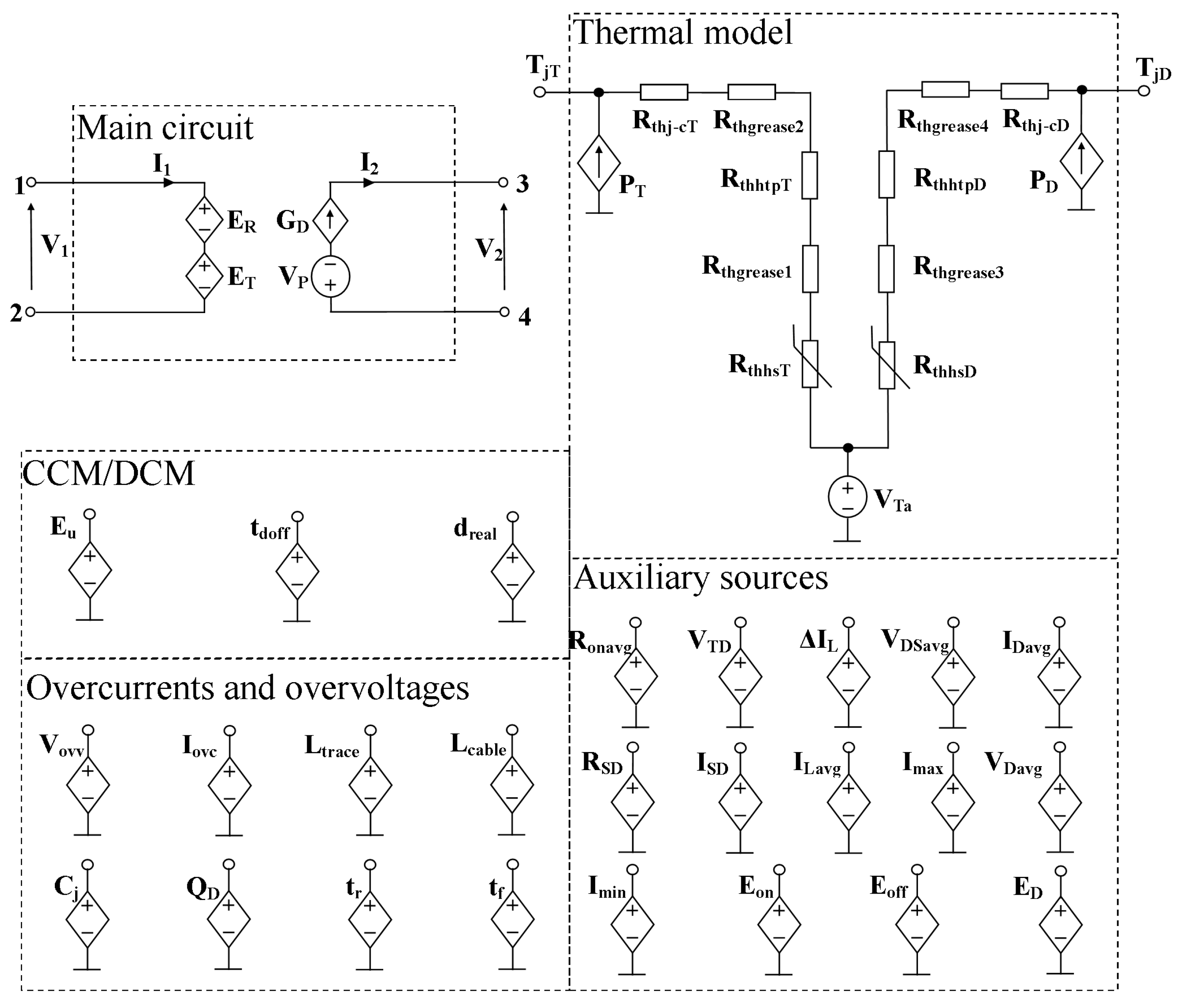
Figure 1. Network representation of the proposed model.
Electronics 13 00154 g001
Figure 2. Flowchart of the parameter estimation procedure of the formulated model.
Electronics 13 00154 g002
Figure 3. Diagram (a) and photo (b) of the measurement setup to determine the characteristics of the buck converter.
Electronics 13 00154 g003
Figure 4. Circuit representation evidencing the main circuit of the proposed electrothermal averaged model of the diode–MOSFET switch.
Electronics 13 00154 g004
Figure 5. Measured and computed output characteristics (a) and corresponding dependences of maximum switched-on current (b), maximum switched-off voltage (c), and junction temperature of diode and MOSFET (d) upon the output current of the converter.
Electronics 13 00154 g005
Figure 6. Measured and computed dependences of output voltage on switching frequency (a) and corresponding dependences of maximum switched-on current (b), maximum switched-off voltage (c), and junction temperature of the MOSFET (d) on switching frequency of the converter.
Electronics 13 00154 g006
Figure 7. Measured and computed waveforms of the drain–source voltage and the drain current.
Electronics 13 00154 g007
Table 1. Values of electrical parameters of the model.
T0 [K]nDISD [fA]RSD [mΩ]VTref [mV]tdoffref [ns]tdon [ns]tdoffdriver [ns]tdondriver [ns]
2981.1307.325.8419210120
aron [K−1]NRSD [K−1]kISD [K−1]bron [K−1]VGShigh [V]aVGS [V]bVGS [V]aID [V/A3]bID [V/A2]
1.17 × 10−66 × 10−49.339 × 10⁻²−9 × 10−618462.25 × 10−64 × 10−5
aIon1 [pJ/A4]aIon2 [nJ/A3]aIon3 [nJ/A3]aIon4 [μJ/A]cRGon [mS]aVD1 [pJ/V2]aVD2 [nJ/V]bVDCon1 [V−2]bVDCon2 [V−1]
−550393−712.39.152877.1785016.28.3 × 10−65.82 × 10⁻⁶
bVDCoff1 [V−2]bVDCoff2 [V−1]cRgoff [mS]aIoff1 [nJ/A2]aIoff2 [nJ/A]RGref [Ω]RGin [Ω]VDCref [V]Cj0 [nF]
1.7 × 10−56.353 × 10−3575.764.5−210.40123002.5
mVj [V]dtr1 [ns/A]dtr2 [ns]dtf1 [ps/A]dtf2 [ns]lt [mm]ht [mm]wt [mm]
0.51.51.674817417.49.278511.54
tt [μm]lc [mm]dc [mm]ref1ref2Ronref [mΩ]tgrease [μm]Rth0 [K/W]agrease [mm2]
35179180.90.1481002.75321
kgrease
[W/m/K]
Rthj-cT [K/W]Rthj-cD
[K/W]
thtp [mm]khtp
[W/m/K]
ahtp [mm2]
2.80.70.5325525
Disclaimer/Publisher’s Note: The statements, opinions and data contained in all publications are solely those of the individual author(s) and contributor(s) and not of MDPI and/or the editor(s). MDPI and/or the editor(s) disclaim responsibility for any injury to people or property resulting from any ideas, methods, instructions or products referred to in the content.