Communication

In-ADC, Rank-Order Filter for Digital Pixel Sensors

by
Miron Kłosowski
1,*,
Yichuang Sun
2,
Waldemar Jendernalik
1,
Grzegorz Blakiewicz
1,
Jacek Jakusz
1 and
Stanisław Szczepański
1
1
Faculty of Electronics Telecommunications and Informatics, Gdańsk University of Technology, 80-233 Gdańsk, Poland
2
School of Engineering and Computer Science, University of Hertfordshire, Hatfield AL10 9AB, UK
*
Author to whom correspondence should be addressed.
Electronics 2024, 13(1), 46; https://doi.org/10.3390/electronics13010046 (registering DOI)
Submission received: 31 October 2023 / Revised: 10 December 2023 / Accepted: 18 December 2023 / Published: 21 December 2023
(This article belongs to the Special Issue Advances in Analog and Mixed-Signal Integrated Circuits)

Abstract

:
This paper presents a new implementation of the rank-order filter, which is established on a parallel-operated array of single-slope (SS) analog-to-digital converters (ADCs). The SS ADCs use an “on-the-ramp processing” technique, i.e., filtration is performed along with analog-to-digital conversion, so the final states of the converters represent a filtered image. A proof-of-concept 64 × 64 array of SS ADCs, integrated with MOS photogates, was fabricated using a standard 180 nm CMOS process. The measurement results demonstrate the full functionality of the novel filter concept, with image acquisition in both single-sampling and correlated-double-sampling (CDS) modes (CDS is digitally performed using ADCs). The experimental, massively parallel rank-order filter can process 650 frames per second with a power consumption of 4.81 mW.

1. Introduction

Digital pixel sensors (DPSs) are a type of CMOS image sensor in which the pixels contain not only analog sensors but also digital hardware. With this capability, DPSs are capable of acquiring and processing images in a fully parallel manner, offering high computational efficiency [1,2,3]. A typical DPS pixel contains a photosensor (with associated analog circuits), an analog-to-digital (AD) converter, and some kind of vision processor. Due to practical reasons, the physical size of the pixel is limited to a few tens of micrometers, so only the simple AD converters of the single-slope (SS) type [4,5,6,7,8,9,10,11,12,13,14,15,16,17] and vision processors with limited resources can be implemented inside the pixels. However, these limited resources are still capable of realizing early-vision algorithms such as convolutional filtration, erosion, dilatation, and median filtering at a speed of thousands of image frames per second and with energy efficiency that exceeds traditional camera-computer systems [1,2,3].
Although DPS sensors are computational and energy-efficient, there are still some limitations related to low-speed SS AD converters that need to be improved. Namely, the relatively simple task of image digitization performed using the SS AD converters takes a longer time compared to the more complex operations of image processing realized in the processors. This problem can be explained as follows.
To digitize an image with N-bit dynamics, SS ADCs need a reference analog ramp signal with 2N steps and the same number of digital clock pulses. Due to analog limitations (i.e., the limited bandwidth of analog comparators in ADCs, delay in distributing the ramp across the entire ADC array), the ramp step cannot be as short as the minimum period of the digital clock, and in practice, the step is extended, e.g., to 10 minimum digital clock periods.
Thus, an additional digital timing budget is available, allowing the clock frequency of the digital part of the ADC to be increased. Extra clock periods can be utilized for image processing. The only operation that needs to be slowed down (e.g., by performing every 10th clock cycle) is capturing the state of the analog comparator. Nevertheless, the combination of two different tasks in one SS ADC comes at the cost of hardware complexity, but the additional processing capability built into this SS ADC compensates for its poor performance related to long digitization time. This technique is referred to as “on-the-ramp processing” since images are processed during digitization in subsequent steps of the reference ramp.
“On-the-ramp processing” was first introduced by us in [11], where we demonstrated an array of SS ADCs capable of linear convolutional filtering. In this paper, however, we propose a new solution suitable for nonlinear rank-order filtering. Since nonlinear filtering involves some special adaptations of the ADC hardware, we developed a new, with respect to [11], 9-bit reversible counter for AD conversion and digital CDS, an additional 5-bit down counter for the rank counting, and a new inter-pixel data exchange procedure. Technical details and measurement results are presented in the following sections.

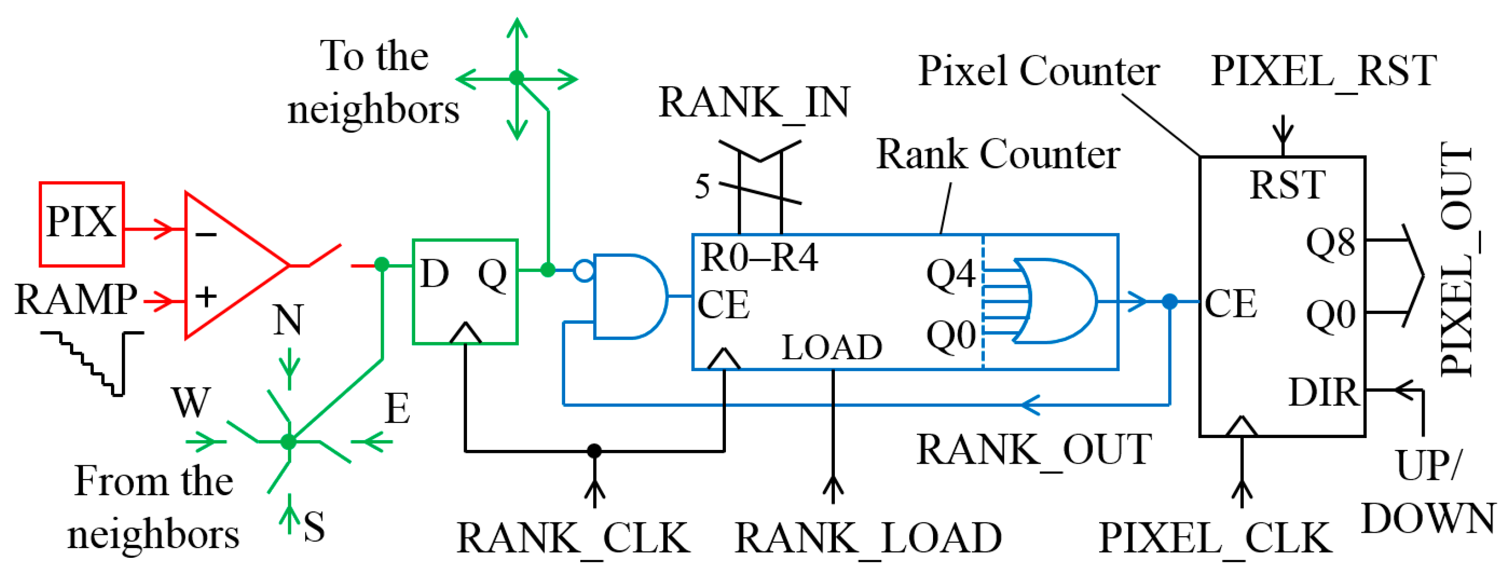
2. Materials and Methods
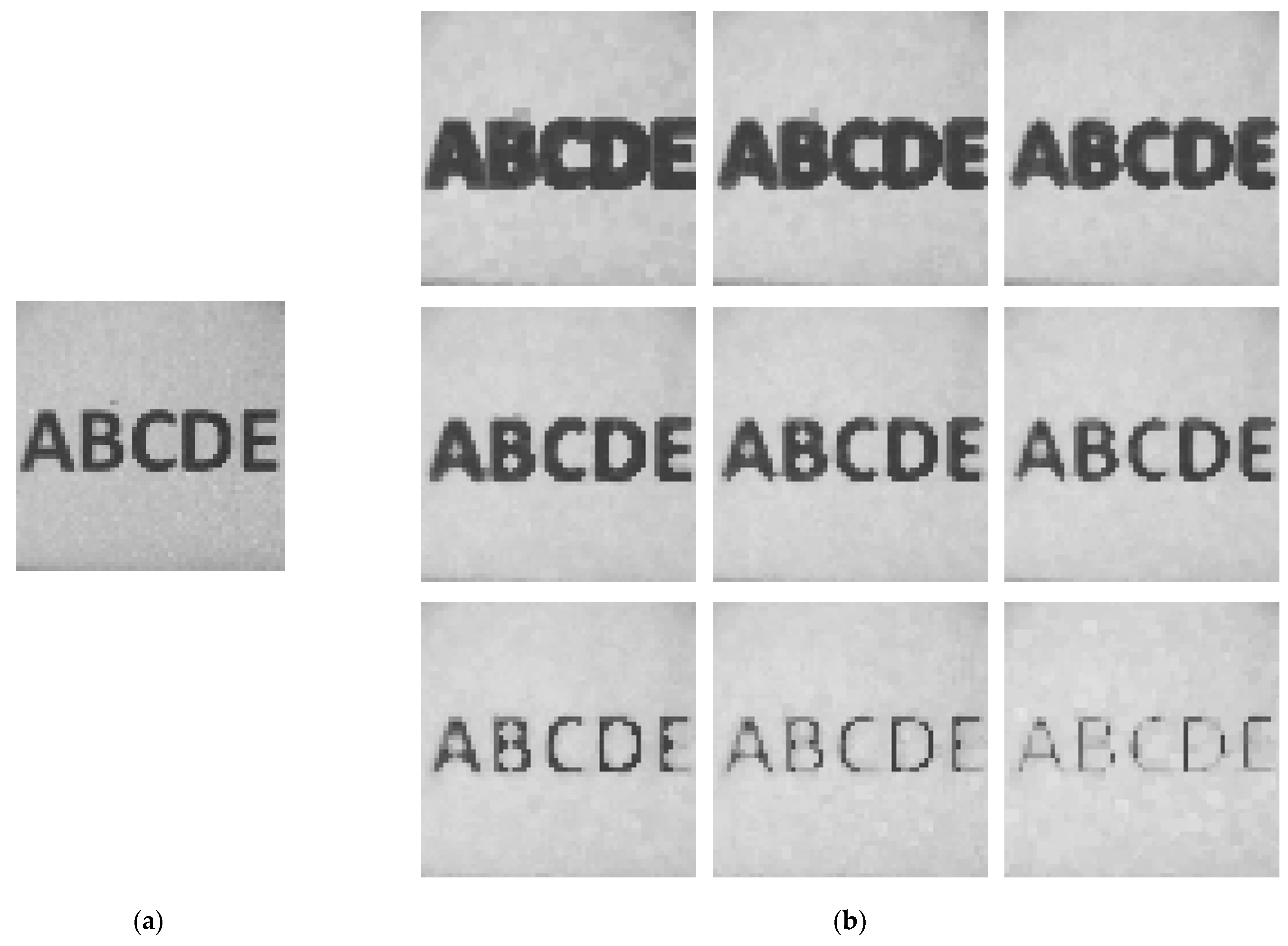
The concept of an SS ADC with a built-in rank-order filter is depicted in Figure 1. The main counter of the ADC is a 9-bit reversible Pixel Counter. It cooperates with a 5-bit down-counting Rank Counter that is loadable through the RANK_IN input. The proposed filter uses the state of the comparators to determine the number of pixels in the neighborhood mask area that have a higher PIX voltage (they are darker) than the current RAMP signal level. To determine the center pixel value after rank-order filtering, it suffices to count (using the Rank Counter) whether the number of pixels in the neighborhood mask that are darker than the current RAMP level has already reached the required rank value (RANK_IN), and on this basis, the center Pixel Counter is stopped (through RANK_OUT signal). The Pixel Counter stops at the value representing the brightness level of the pixel that turned out to be the nth pixel in the filter mask area (where n is the rank value) whose comparator output has changed to a low logical level. Flip-flops storing the current state of comparators in pixels are interconnected and create a programmable 2D shift register. This makes it easy to count how many neighboring comparators have already reached a low logical level.
The complete implementation of the concept is presented in Figure 2. The rank-order processing for a given level of the RAMP signal starts with a pulse on the ϕSELF signal. Then, ϕ2 and ϕSTAT are activated so that the latch, built from G1 and G2 inverters, can overcome the metastable state. A pulse on the RANK_LOAD signal then loads the initial Rank Counter value from the data bus. During the processing, the bidirectional data bus contains the initial value of the Rank Counter. The data bus is driven from outside the imager and determines the rank level realized by the filter.
Using the RANK_CLK and ϕ2 pulses, the state of the comparator for the center pixel is counted. Then, a pulse is generated on ϕN, ϕE, ϕS, or ϕW depending on the shift direction of the 2D shift register. The state of the adjacent comparator that now appeared in the register composed of G1 and G2 after the previous 2D shift is counted now. This process is repeated until the states of all the comparators from the filter neighborhood mask are counted. The Rank Counter counts the number of adjacent pixels that are darker than the currently processed RAMP level (low logic level of the comparator) and has a mechanism that disables it after counting down to zero. Finally, with the RANK_EVAL signal, the status of the Rank Counter is checked, and if it is zero, the Pixel Counter is blocked. The signal waveforms for a 3 × 3 neighborhood mask related to this process are shown in Figure 3.
The detailed schematic diagram of the Rank Counter is shown in Figure 4a. Rank Counter is based on an XNOR Fibonacci linear feedback shift register (LFSR) to reduce the layout area. The final zero state is detected through dynamic logic and stops the counter. The initial counter value driven from the RANK_IN bus is encoded in the LFSR code through external hardware. The counter works with a high clock frequency; therefore, simple dynamic latches are used. The diagram of these latches is shown in Figure 4b. The clock is three-phase, formed by the following pulses: ϕNESW, RANK_CLK, and ϕ2. The cycle of this clock is 50 ns. Nine clock cycles are required to perform the rank calculation on the 3 × 3 neighborhood mask for a given RAMP level, with one extra clock needed for the evaluation, which yields the duration of a single RAMP level at approximately 500 ns. The converter needs 512 levels (i.e., steps) of the RAMP signal, which provides a processing time of 256 μs. The minimum duration of a RAMP step is about 400 ns (determined experimentally). Reducing this period causes a significant deterioration in the conversion quality due to the limited speed of analog circuits, especially the comparators. In the proposed rank-order 3 × 3 converter, this time is only slightly longer (500 ns) due to the operation of the Rank Counter.
All neighborhood mask shapes are possible, but for certain mask shapes (cross-shaped, for example), it may be necessary to “visit” some pixels several times or to “visit” pixels that are not in the mask. In such cases, the second phase of the clock (RANK_CLK signal) is not pulsed to prevent the incorrect position from being included in the rank calculation.
The binary Pixel Counter (Figure 5a) consists of nine identical stages, as shown in Figure 5b. The signals ϕ2, ϕSTAT, RST, UP, and DOWN are common to all stages. UP and DOWN signals facilitate counting in both directions, which is important for correlated double sampling (CDS) operations. The RANK_EVAL signal is used to count the results of the pixel rank-order filter, while the RANK_BYPASS signal allows for simple conversion without filtering.
Assuming AD conversion with no filtering, CDS can be digitally implemented by changing the counting direction of the Pixel Counter. After a pulse on RG, the counter counts backward, and after a pulse on TG, it counts forward. If a linear operation, e.g., convolution, is additionally performed during the AD conversion, digital CDS can still be performed in this way by changing the sign of the linear operation between conversions (by reversing the counting direction)—according to the superposition rule [11].
Rank-order filtering is not a linear operation, and therefore, the principle of superposition does not apply. So, if digital CDS is performed simultaneously with rank-order filtering, it will not yield a perfect result. Ideally, CDS should be performed entirely on the analog side, and then a single AD conversion with rank-order filtering can be performed. Nevertheless, measurements indicate a satisfactory reduction of fixed-pattern noise (FPN) through the CDS implemented with simultaneous rank-order filtering, as shown in the next section.
The presented method of rank-order filtering requires special treatment of signals passing through the edges of the pixel matrix. However, in our experimental DPS imager, there is no such mechanism. The edge-crossing outputs are open, and the edge-crossing inputs are grounded. This makes the 2-dimensional shift operation incomplete (edge data are lost), and thus, the resulting image is distorted near the borders. The suggested solution is to use dummy pixels on the edge of the imager with only shift register functionality (only G1, G2, and switches). Analog circuits, rank, and pixel counters are not needed. The switch ϕSELF in dummy pixels is proposed to be connected to the global signal specifying the illumination level of dummy pixels (GLOBAL_EDGE_LEVEL). Figure 6 shows a diagram and waveforms of dummy pixels set to an emulated illumination level. This level is determined through the level of the RAMP signal at the moment of the falling edge of the GLOBAL_EDGE_LEVEL signal (in the case of CDS, the additional falling edge determines the pixel reset level).
In the presented DPS, an off-chip crop edge handling method has been used; hence, acquired images are smaller (60 × 60) than the full size of the imager (64 × 64).

3. Results

The proof-of-concept imager chip was fabricated using the standard 0.18 μm 1P6M CMOS process of ams AG (austriamicrosystems). The photo of the chip is presented in Figure 7a. The pixel size is 55 μm × 55 μm. Only part of the pixel area is used in this work. Utilized modules are named and marked in Figure 7b, while the rest are intended for other projects.
Figure 8b presents the results of image acquisition with digital CDS using the 3 × 3 rank-order filter, with the rank ranging from 1 to 9, respectively. The result of the median filter (rank 5) is presented in the central image. For comparison, the original picture acquired with the rank-order filter disabled is shown in Figure 8a. Figure 8 shows that the rank-order filter works correctly for all ranks.
Measurements of the imager with variable uniform irradiation were also performed. The average response of the pixel is presented in Figure 9. The graph shows that the image sensor is linear when digital CDS is performed. As expected, median filtering (MF) does not affect the average pixel response.
Figure 10 shows the graph of FPN vs. irradiance. The effect of median filtering is most noticeable when CDS is turned off. In fact, when CDS is on, most of the dark-signal non-uniformity (DSNU) noise is already removed by the CDS itself. However, with CDS enabled, the median filter operation becomes visible again for higher irradiance because additional photo-response non-uniformity (PRNU) noise emerges, which is reduced through the median filter. In addition, FPN was measured for an off-chip software median filter implementation processing the response of the imager with CDS turned on (e). The graph shows a slight reduction in noise compared to the median filter integrated with the imager (d). This reduction is due to the previously mentioned imperfection of the digital CDS performed simultaneously with rank-order filtering. Ideally, the CDS conversion combined with rank-order filtering should be implemented according to the following formula:
I m a g e o u t p u t = R a n k O r d e r I m a g e p h o t o I m a g e r e s e t .
However, in the presented imager, this can only be performed according to the following formula:
I m a g e o u t p u t = R a n k O r d e r ( I m a g e p h o t o ) R a n k O r d e r ( I m a g e r e s e t ) .
Figure 11 shows the results of different combinations of CDS and median filtering. The lowest FPN level and the best picture quality are observed in (d), where digital CDS is enabled simultaneously with the median filter.
Interesting results can be obtained by changing the rank order parameter during image conversion. Halfway through the ADC processing time (halfway through the ramp signal), the rank order value (initial value of the rank counter) changes from 1 (minimum filter) to 9 (maximum filter). The effects of such an operation can be observed in Figure 12d. For comparison, the image without modification (Figure 12a) and images captured with a static rank (minimum filter in Figure 12b and maximum filter in Figure 12c) are also shown. As shown in Figure 12d, the effects of minimum and maximum filters were combined in such a way that the enlargement of the surface of objects (dilation) worked for both dark objects on a light background and light objects on a dark background. This is impossible for filters with a fixed rank order (Figure 12b,c). The disadvantage of this technique is lower contrast and higher image noise.
The measured energy per conversion with CDS for the digital part of a single pixel in dark condition is as follows: 17.6 pJ for a simple conversion, 82 pJ for the minimum 3 × 3 filter (rank 1), 229 pJ for the median 3 × 3 filter (rank 5), and 404 pJ for the maximum 3 × 3 filter (rank 9). The same measured in bright condition (250 mW/m2, 625 nm) is as follows: 35.2 pJ for a simple conversion, 99.6 pJ for the minimum 3 × 3 filter (rank 1), 211 pJ for the median 3 × 3 filter (rank 5), and 328 pJ for the maximum 3 × 3 filter (rank 9). The analog circuits consume a constant power of about 220 nW per pixel.
The rank-order neighborhood mask is not limited, but above 3 × 3, it may affect the maximum frame rate. A 3 × 3 neighborhood requires 10 clock cycles and allows a frame rate of 650 fps with digital CDS, whereas a 5 × 5 neighborhood needs 26 clock cycles, which reduces the frame rate to approximately 250 fps with digital CDS. The maximum possible rank value in our design is 30 and is limited only by the capacity of the Rank Counter. For example, it is possible to perform 7 × 7 median filtering by setting the initial value of the Rank Counter to 25, but the 7 × 7 maximum filter is not achievable.

4. Discussion

Table 1 presents the recent proof-of-concept DPS imagers with built-in pixel-level processing. The DPSs [7,8] are smart sensors that offer various algorithms (thresholding, convolution, edge detection, histogram, etc.) thanks to the pixel-level processors with a general-purpose-type architecture (ALUs, registers, etc.). In turn, in [9,11] and in this work, the imagers do not use processors but SS AD converters adapted for image processing. These modified converters are capable of performing one selected algorithm, but this algorithm is performed on the ramp during the AD conversion procedure, which saves the overall system operation time. In terms of energy, the on-the-ramp solutions [9,11] and this work show an energy figure (pJ/pix/frame) that is better than [7,8]. The best figure is achieved through the sensor [9], but its converters perform a relatively simple pixel gain-correction algorithm (through the clock-stopping mechanism that additionally reduces energy consumption). The proposed on-the-ramp data processing technique can also be adapted for implementation in image sensors with SS ADCs operating in time or hybrid mode [10,18,19]. For proper operation in time or hybrid mode, ADC linearity must be assured (e.g., using a variable ADC clock frequency). There are also similar image processing solutions in column-parallel SS AD converters [20,21,22].
An interesting extension of the presented technique is the imager in which the CDS is implemented entirely in the analog domain, i.e., prior to AD conversion. In this case, there is no problem with the imperfect operation of the CDS mechanism working simultaneously with the rank-order filter, and there is the possibility of repeating the processing of the same image many times with different rank values and/or neighborhood masks. It is also possible to implement a dynamic rank mechanism by quickly changing the value on the RANK_IN bus during processing.

5. Conclusions

The proposed solution of a two-dimensional rank-order filter integrated with an array of single-slope AD converters allows for performing a filtering operation during the AD conversion without a significant impact on the duration of this conversion. If this filter were implemented outside the ADC array as an additional circuit, it would take additional time for processing, so the proposed solution reduces latency. Moreover, the filtering operation performed during SS-type AD conversion allows access to information about the pixel brightness in the form of pulse duration. In the time domain, the pixel brightness comparison operation can be implemented using a simple logic gate. Therefore, the chip area and power consumption are smaller than if a rank-order filtering operation were performed on binary data, where complex digital comparators are required. The practical significance of the proposed solution covers all low-power 2D sensors whose results are, in the first stage, subject to rank-order filtering. As a direction for further research, an attempt can be made to create a filter integrated with the AD converter, allowing for subsequent filtration operations to be performed on an already filtered image (e.g., this would enable morphological opening and closing operations).
The proposed in-ADC solution of the rank-order filter can be used in single-chip and layered CMOS image sensors with a global shutter, especially when low power consumption, high image sensor integration, and low latency are required. Moreover, it can be applied in various types of intelligent image sensors, where it is essential, for example, to denoise the image before further processing. These types of sensors are used in monitoring and security systems [23]. Low-power devices such as IoT can also take advantage of the presented solution [24]. Furthermore, it can be used to precondition images before being processed using a deep neural network [25,26,27].

Author Contributions

Conceptualization, M.K. and Y.S.; methodology, M.K. and Y.S.; software, M.K.; validation, J.J., G.B. and W.J.; formal analysis, Y.S.; investigation, M.K.; writing—original draft preparation, M.K. and W.J.; writing—review and editing, M.K. and W.J.; visualization, M.K.; supervision, S.S.; project administration, W.J.; funding acquisition, S.S., W.J., M.K., G.B. and J.J. All authors have read and agreed to the published version of the manuscript.

Funding

This research was funded in part by the National Science Centre of Poland, grant number 2016/23/B/ST7/03733.

Data Availability Statement

Data are contained within the article.

Conflicts of Interest

The authors declare no conflict of interest. The funders had no role in the design of this study; in the collection, analyses, or interpretation of data; in the writing of the manuscript; or in the decision to publish the results.

References

  1. Dudek, P.; Richardson, T.; Bose, L.; Carey, S.; Chen, J.; Greatwood, C.; Liu, Y.; Mayol-Cuevas, W. Sensor-level computer vision with pixel processor arrays for agile robots. Sci. Robot. 2022, 7, 67. [Google Scholar] [CrossRef] [PubMed]
  2. Lefebvre, M.; Moreau, L.; Dekimpe, R.; Bol, D. A 0.2-to-3.6 TOPS/W programmable convolutional imager SoC with in-sensor current-domain ternary-weighted MAC operations for feature extraction and region-of-interest detection. In Proceedings of the IEEE International Solid-State Circuits Conference (ISSCC), San Francisco, CA, USA, 13 February 2021; pp. 118–120. [Google Scholar] [CrossRef]
  3. Ishikawa, M. High-speed Image Processing Devices and Its Applications. In Proceedings of the IEEE International Electron Devices Meeting (IEDM), San Francisco, CA, USA, 7 December 2019; pp. 10.7.1–10.7.4. [Google Scholar] [CrossRef]
  4. Ikeno, R.; Mori, K.; Uno, M.; Miyauchi, K.; Isozaki, T.; Takayanagi, I.; Nakamura, J.; Wuu, S.-G.; Bainbridge, L.; Berkovich, A.; et al. A 4.6-μm, 127-dB Dynamic Range, Ultra-Low Power Stacked Digital Pixel Sensor with Overlapped Triple Quantization. IEEE Trans. Electron Devices 2022, 69, 2943–2950. [Google Scholar] [CrossRef]
  5. Seo, M.-W.; Chu, M.; Jung, H.-Y.; Kim, S.; Song, J.; Bae, D.; Lee, S.; Lee, J.; Kim, S.-Y.; Lee, J.; et al. 2.45 e-RMS Low-Random-Noise, 598.5 mW Low-Power, and 1.2 kfps High-Speed 2-Mp Global Shutter CMOS Image Sensor with Pixel-Level ADC and Memory. IEEE J. Solid-State Circuits 2022, 57, 1125–1137. [Google Scholar] [CrossRef]
  6. Sakakibara, M.; Ogawa, K.; Sakai, S.; Tochigi, Y.; Honda, K.; Kikuchi, H.; Wada, T.; Kamikubo, Y.; Miura, T.; Nakamizo, M.; et al. A 6.9-μm Pixel-Pitch Back-Illuminated Global Shutter CMOS Image Sensor with Pixel-Parallel 14-Bit Subthreshold ADC. IEEE J. Solid-State Circuits 2018, 53, 3017–3025. [Google Scholar] [CrossRef]
  7. Schmitz, J.A.; Gharzai, M.K.; Balkır, S.; Hoffman, M.W.; White, D.J.; Schemm, N. A 1000 frames/s Vision Chip Using Scalable Pixel-Neighborhood-Level Parallel Processing. IEEE J. Solid-State Circuits 2017, 52, 556–568. [Google Scholar] [CrossRef]
  8. Millet, L.; Chevobbe, S.; Andriamisaina, C.; Benaissa, L.; Deschaseaux, E.; Beigne, E.; Ben Chehida, K.; Lepecq, M.; Darouich, M.; Guellecet, F.; et al. A 5500-frames/s 85-GOPS/W 3-D Stacked BSI Vision Chip Based on Parallel In-Focal-Plane Acquisition and Processing. IEEE J. Solid-State Circuits 2019, 54, 1096–1105. [Google Scholar] [CrossRef]
  9. Kłosowski, M.; Jendernalik, W.; Jakusz, J.; Blakiewicz, G.; Szczepański, S. A CMOS pixel with embedded ADC, digital CDS and gain correction capability for massively parallel imaging array. IEEE Trans. Circuits Syst. I Regul. Pap. 2017, 64, 38–49. [Google Scholar] [CrossRef]
  10. Kłosowski, M.; Sun, Y. Fixed Pattern Noise Reduction and Linearity Improvement in Time-Mode CMOS Image Sensors. Sensors 2020, 20, 5921. [Google Scholar] [CrossRef] [PubMed]
  11. Kłosowski, M.; Sun, Y.; Jendernalik, W.; Blakiewicz, G.; Jakusz, J.; Szczepański, S. Single-Slope ADC with Embedded Convolution Filter for Global-Shutter CMOS Image Sensors. IEEE Trans. Circuits Syst. II Express Briefs 2023, 70, 3258–3262. [Google Scholar] [CrossRef]
  12. Son, S.; Jeon, S.; Namgung, S.; Yoo, J.; Song, M. A one-shot digital correlated double sampling with a differential difference amplifier for a high speed CMOS image sensor. In Proceedings of the 2015 IEEE International Symposium on Circuits and Systems (ISCAS), Lisbon, Portugal, 24 May 2015; pp. 1054–1057. [Google Scholar] [CrossRef]
  13. Wei, J.; Li, X.; Sun, L.; Li, D. A Low-Power Column-Parallel Gain-Adaptive Single-Slope ADC for CMOS Image Sensors. Electronics 2020, 9, 757. [Google Scholar] [CrossRef]
  14. Agarwal, A.; Hansrani, J.; Bagwell, S.; Rytov, O.; Shah, V.; Ong, K.L.; Blerkom, D.V.; Bergey, J.; Kumar, N.; Lu, T.; et al. A 316MP, 120FPS, High Dynamic Range CMOS Image Sensor for Next Generation Immersive Displays. Sensors 2023, 23, 8383. [Google Scholar] [CrossRef] [PubMed]
  15. Yamazaki, T.; Katayama, H.; Uehara, S.; Nose, A.; Kobayashi, M.; Shida, S.; Odahara, M.; Takamiya, K.; Hisamatsu, Y.; Matsumoto, S.; et al. 4.9 A 1ms high-speed vision chip with 3D-stacked 140GOPS column-parallel PEs for spatio-temporal image processing. In Proceedings of the IEEE International Solid-State Circuits Conference (ISSCC), San Francisco, CA, USA, 5 February 2017; pp. 82–83. [Google Scholar] [CrossRef]
  16. Okura, S.; Nishikido, O.; Sadanaga, Y.; Kosaka, Y.; Araki, N.; Ueda, K.; Morishita, F. A 3.7 M-pixel 1300-fps CMOS image sensor with 5.0 G-pixel/s high-speed readout circuit. IEEE J. Solid-State Circuits 2015, 50, 1016–1024. [Google Scholar] [CrossRef]
  17. Liu, C.; Bainbridge, L.; Berkovich, A.; Chen, S.; Gao, W.; Tsai, T.H.; Mori, K.; Ikeno, R.; Uno, M.; Isozaki, T.; et al. A 4.6 μm 512 × 512 ultra-low power stacked digital pixel sensor with triple quantization and 127dB dynamic range. In Proceedings of the IEEE International Electron Devices Meeting (IEDM), San Francisco, CA, USA, 12 December 2020; pp. 16.1.1–16.1.4. [Google Scholar] [CrossRef]
  18. Kłosowski, M. Hybrid-mode single-slope ADC with improved linearity and reduced conversion time for CMOS image sensors. Int. J. Circuit Theory Appl. 2020, 48, 28–41. [Google Scholar] [CrossRef]
  19. Isozaki, T.; Mori, K.; Miyauchi, K.; Uno, M.; Ikeno, R.; Takayanagi, I.; Nakamura, J.; Wuu, S.-G.; Berkovich, A.; Chen, S.; et al. 110 dB high dynamic range continuous non-uniform TTS and linear ADC scheme using a 4.6 μm stacked digital pixel sensor. In Proceedings of the 2023 International Image Sensor Workshop, Scotland, UK, 21–25 May 2023. R4.4. [Google Scholar]
  20. Jin, M.; Noh, H.; Song, M.; Kim, S.Y. Design of an Edge-Detection CMOS Image Sensor with Built-in Mask Circuits. Sensors 2020, 20, 3649. [Google Scholar] [CrossRef] [PubMed]
  21. Lee, S.; Jeong, B.; Park, K.; Song, M.; Kim, S.Y. On-CMOS Image Sensor Processing for Lane Detection. Sensors 2021, 21, 3713. [Google Scholar] [CrossRef] [PubMed]
  22. Valenzuela, W.; Saavedra, A.; Zarkesh-Ha, P.; Figueroa, M. Motion-Based Object Location on a Smart Image Sensor Using On-Pixel Memory. Sensors 2022, 22, 6538. [Google Scholar] [CrossRef] [PubMed]
  23. Sukhavasi, S.B.; Sukhavasi, S.B.; Elleithy, K.; Abuzneid, S.; Elleithy, A. CMOS Image Sensors in Surveillance System Applications. Sensors 2021, 21, 488. [Google Scholar] [CrossRef]
  24. Choo, K.D.; Xu, L.; Kim, Y.; Seol, J.H.; Wu, X.; Sylvester, D.; Blaauw, D. Energy-Efficient Motion-Triggered IoT CMOS Image Sensor with Capacitor Array-Assisted Charge-Injection SAR ADC. IEEE J. Solid-State Circuits 2019, 54, 2921–2931. [Google Scholar] [CrossRef]
  25. Zheng, X.; Cheng, L.; Zhao, M.; Luo, Q.; Li, H.; Dou, R.; Yu, S.; Wu, N.; Liu, L. Vip: A Hierarchical Parallel Vision Processor for Hybrid Vision Chip. IEEE Trans. Circuits Syst. II Express Briefs 2022, 69, 2957–2961. [Google Scholar] [CrossRef]
  26. Eki, R.; Yamada, S.; Ozawa, H.; Kai, H.; Okuike, K.; Gowtham, H.; Nakanishi, H.; Almog, E.; Livne, Y.; Yuval, G.; et al. 9.6 A 1/2.3inch 12.3Mpixel with on-chip 4.97TOPS/W CNN processor back-illuminated stacked CMOS image sensor. In Proceedings of the IEEE International Solid-State Circuits Conference (ISSCC), San Francisco, CA, USA, 13 February 2021; pp. 154–156. [Google Scholar] [CrossRef]
  27. Amir, M.F.; Ko, J.H.; Na, T.; Kim, D.; Mukhopadhyay, S. 3-D Stacked Image Sensor with Deep Neural Network Computation. IEEE Sens. J. 2018, 18, 4187–4199. [Google Scholar] [CrossRef]
Figure 1. Concept of the proposed pixel. The analog signal path is marked in red, the 2D shift register path is marked in green, and the rank calculation circuit is marked in blue.
Electronics 13 00046 g001
Figure 2. Complete implementation of the proposed pixel. The analog signal path is marked in red, the 2D shift register path is marked in green, and the rank calculation circuit is marked in blue.
Electronics 13 00046 g002
Figure 3. Sample waveforms of the presented rank-order filter.
Electronics 13 00046 g003
Figure 4. Rank Counter: (a) register-level diagram; (b) the register.
Electronics 13 00046 g004
Figure 5. Pixel Counter: (a) stage-level diagram; (b) the stage.
Electronics 13 00046 g005
Figure 6. Example of edge handling—schematic diagram and waveforms.
Electronics 13 00046 g006
Figure 7. Imager: (a) photo; (b) pixel layout (Cadence view).
Electronics 13 00046 g007
Figure 8. Images captured: (a) with the rank-order filter disabled and (b) using a 3 × 3 rank-order filter for ranks 1–9 (respectively).
Electronics 13 00046 g008
Figure 9. Pixel response measured for image acquisition without CDS (a,b), with CDS (c,d), without median filtering (a,c), and with median filtering (b,d).
Electronics 13 00046 g009
Figure 10. FPN measured for image acquisition without CDS (a,b), with CDS (c–e), without median filtering (a,c), with median filtering (b,d), and with off-chip software median filtering (e).
Electronics 13 00046 g010
Figure 11. Images captured: (a) without any processing (raw image), (b) using a 3 × 3 median filter, (c) using digital CDS, and (d) using digital CDS and a 3 × 3 median filter simultaneously.
Electronics 13 00046 g011
Figure 12. Images captured: (a) without filtering, (b) using a 3 × 3 minimum filter, (c) using a 3 × 3 maximum filter, and (d) using a 3 × 3 dynamic rank order filter.
Electronics 13 00046 g012
Table 1. Recent DPSs with pixel-level processing.
Ref. [7] Schmitz
2017
Ref. [8] Millet
2019
Ref. [9] Kłosowski
2017
Ref. [11] Kłosowski 2023This Work
Vision algorithmsmanymanypixel gain correction (PRNU compensation)convolution filteringall rank-order filtering
Vision processors8-bit neighborhood processors (NPs)8-bit processing elements (PEs)9-bit modified
SS ADCs
9-bit modified
SS ADCs
9-bit modified
SS ADCs
CMOS process0.13 FSI0.13 BSI 3D0.18 FSI0.18 FSI0.18 FSI
Supply, V2.5/1.21.21.8/1.21.8/1.21.8/1.2
Pixel array80 × 641024 × 768128 × 12864 × 6464 × 64
Grayscale8b9–11b9b9b9b
Dynamic range, dB54484949
Max. FPS with CDS10005500 (1)35001000650
Power, mW36720 (1)286.75 (2.3 (2))4.81 (1.9 (2))
pJ/pix/frame700026184861647 (557 (2))1807 (704 (2))
Pixel pitch, μm39.612215555
Fill factor, %12755.510.910.9
(1) At 0.05 Mpix, 9 bits. (2) Array core.
Disclaimer/Publisher’s Note: The statements, opinions and data contained in all publications are solely those of the individual author(s) and contributor(s) and not of MDPI and/or the editor(s). MDPI and/or the editor(s) disclaim responsibility for any injury to people or property resulting from any ideas, methods, instructions or products referred to in the content.

