Article

Compact and Hybrid Dual-Band Bandpass Filter Using Folded Multimode Resonators and Second-Mode Suppression

by
Nicolas Claus
*,
Kamil Yavuz Kapusuz
,
Jo Verhaevert
* and
Hendrik Rogier
Department of Information Technology, Ghent University-imec, Technologiepark-Zwijnaarde 126, 9052 Ghent, Belgium
*
Authors to whom correspondence should be addressed.
Electronics 2024, 13(10), 1921; https://doi.org/10.3390/electronics13101921
Submission received: 16 April 2024 / Revised: 6 May 2024 / Accepted: 10 May 2024 / Published: 14 May 2024
(This article belongs to the Section Microwave and Wireless Communications)

Abstract

:
The proliferation of the Internet of Things (IoT) propels the continuous demand for compact, low-cost, and high-performance multiband filters. This paper introduces a novel low-profile dual-band bandpass filter (BPF) constructed with a back-to-back coupled pair of shielded folded quarter-mode substrate integrated waveguide (SF-QMSIW) multimode cavities. A hybrid structure is obtained by etching a coplanar waveguide (CPW) coupling line in the folded cavity’s septum layer. It serves multiple functions: generating an additional resonance, providing a separate coupling mechanism for the upper passband, and offering the flexibility to control the passbands’ center frequency ratio. Additionally, the unused second higher-order mode is suppressed by integrating embedded split-ring resonators (ESRRs) with an inter-digital capacitor (IDC) structure into the feed lines. A filter prototype has been fabricated and experimentally tested. The measurements confirmed reliable operation in two passbands having center frequencies 3.6 GHz and 5.8 GHz, and exhibiting 3 dB fractional bandwidths (FBWs) of 6.4% and 5.3%, respectively. Furthermore, the group delay variation within both passbands equals only 0.62 ns and 1.00 ns, respectively. Owing to the second higher-order mode suppression, the filter demonstrated an inter-band rejection exceeding 38 dB, within a compact footprint of 0.71 λ g 2 (with λ g being the guided wavelength at the lower passband’s center frequency).

1. Introduction

Rapid advances in the field of wireless communications have stimulated the proliferation of interconnected devices and the swift expansion of the Internet of Things (IoT). By connecting millions of physical devices to the internet and providing ubiquitous sensing and computing capabilities, the IoT has revolutionized our daily lives. This unlocks enormous potential for the development of future applications that enhance the quality of life and are intriguing both for academia and industry [1]. In the last decade, fifth generation (5G) mobile networks have been the enabling technology for the remarkable growth of the IoT ecosystem, owing to their unprecedented bandwidth, reliability, and ultra-low latency [2]. However, as we glimpse what lies ahead, the advent of sixth generation (6G) communication systems is expected to integrate artificial intelligence (AI)-powered capabilities and edge computing [3,4]. These applications require the exchange of vast amounts of data. Moreover, to ensure efficient operation and provide seamless connectivity within the IoT ecosystem, such systems require robust and reliable communication channels.
One of the most important components in a communication channel is the bandpass filter (BPF): it serves as a gatekeeper, allowing only specific frequencies to pass through, while others are rejected or attenuated. Especially in the dynamic and congested radio frequency (RF) environments that are typical for IoT deployments, BPFs play a pivotal role. They minimize the interference from coexisting wireless networks and from ambient electromagnetic noise. However, due to the inherent heterogeneity of the IoT ecosystem, multiple standards with diverse frequencies are used across different IoT applications. A prime example of a challenging RF environment is found in the context of autonomous vehicles. Self-driving cars are equipped with several antenna systems, operating across various frequency bands. These wireless systems enable the vehicle to sense its surroundings, communicate with its environment, and become an integral part of the interconnected IoT landscape. To accommodate the desired frequencies and reject undesired ones, high-performance BPFs are indispensable. Traditional single-band filters, while effective within their designated frequency ranges, fall short of accommodating these diverse spectrum requirements. Hence, multiband or dual-band BPFs are required. For optimal versatility, these filters should ideally support both licensed and unlicensed frequency bands, as well as cellular and non-cellular standards. Another important requirement is related to the size. To facilitate inconspicuous integration into a car’s sleekly designed dashboard, wireless components with a small form factor are required. Hence, compact, lightweight, and low-cost BPFs that cover multiple frequency bands are considered a research hotspot [5,6].
Microstrip technology has proven its value for the realization of filters, owing to its simple structure, low fabrication cost, and straightforward integration of resonant stubs and step impedance resonators (SIRs) [7,8,9]. However, due to the moderate power handling capability, high radiation loss, and fabrication concessions at microwave frequencies [10], other technologies have been explored to construct high-performance microwave components. In particular, substrate integrated waveguide (SIW) technology has emerged as an excellent alternative, offering a shielded structure, low loss, high Q-factor, high power handling capability, and easy integration with planar circuits [10,11]. Moreover, due to its compatibility with standard printed circuit board (PCB) manufacturing processes, it is considered a cost-effective solution [12]. To miniaturize SIW-based filters while preserving the original SIW characteristics and field distributions, several techniques have been proposed. These include the half-mode substrate integrated waveguide (HMSIW) [13,14,15,16,17,18], quarter-mode substrate integrated waveguide (QMSIW) [19,20], eighth-mode substrate integrated waveguide (EMSIW) [11,21,22,23], and sixteenth-mode substrate integrated waveguide (SMSIW) [24,25] topologies. To limit the radiation loss and preserve a moderate Q-factor, shielded versions have been suggested [26,27,28]. Another miniaturization strategy consists of exploiting multilayer structures, such as the folded substrate integrated waveguide (FSIW) [29,30] or the folded ridged substrate integrated waveguide (FRSIW) [31]. These topologies may be combined with HMSIW or QMSIW cavities to achieve further size reduction [32,33].
In recent literature, much research has been conducted on high-performance, compact, low-cost, and low-loss SIW dual-band or multiband filters. The most prevalent design strategies can be divided into four categories. First, the most straightforward method consists of combining multiple independent single-band BPFs [34,35]. However, the inherent bulkiness of the resulting structures hinders their practical application for size-constrained use cases. Another method is based on the coupled matrix synthesis technique. It consists of dividing a wide passband into several sub-bands through the well-controlled introduction of transmission zeros (TZs) [36,37,38,39]. Yet, since the passbands need to be close to each other, this method is often not applicable to multiband scenarios where the operating frequencies are more widely spaced. Third, multimode resonators (MMRs) have been introduced to exploit multiple (perturbed) resonances, resulting from the fundamental and higher-order modes, in a single cavity [40,41,42,43,44,45,46,47,48]. Although this strategy can yield compact structures, it is generally hard to control the passbands and stopbands originating from the different modes independently. Finally, hybrid structures have been suggested, which merge the advantages of SIW-based cavity filters with other technologies, such as microstrips, slotlines, or coplanar waveguides (CPWs) [18,49,50,51,52,53,54,55]. These hybrid filter topologies provide greater design flexibility while maintaining a compact size. However, the etching of slots in outer copper layers can compromise the shielding integrity of the SIW structure.
In this paper, a novel compact dual-band BPF is proposed for deployment in autonomous vehicles. It is based on a pair of shielded, folded, and back-to-back positioned QMSIW multimode cavities. A hybrid structure is obtained by etching a CPW half-wavelength resonator in the folded cavity’s septum layer. The lower passband is constructed from the fundamental cavity modes. In addition, the upper passband exploits both the third-order resonant cavity modes and the resonance from the CPW half-wavelength resonator. Two different coupling structures, namely, an inductive window and a CPW coupling trace, are exploited to separately control the coupling for the lower and upper passband, respectively. Hence, a dual-band filter is constructed that combines the merits of the aforementioned MMR and hybrid design strategies. The resonant elements in the filter provide semi-independent coupling mechanisms. Yet, they do not degrade the SIW shielding nature since etching is performed on the folded structure’s inner layers. To the best of the authors’ knowledge, it is the first time that such a hybrid multimode dual-band design strategy has been leveraged within a folded SIW cavity structure. Additionally, to improve the inter-band rejection between the lower and upper passband, the unused second-order cavity mode is suppressed using embedded split-ring resonators (ESRRs) in the feed lines. The design of these ESRRs is inspired by [56]. However, they are modified with an inter-digital capacitor (IDC) structure to avoid the need for lossy active or passive components.
This manuscript is organized as follows. The following section presents the structure of the shielded and folded QMSIW cavity, which is the building block for the proposed filter. Section 3 discusses the proposed dual-band BPF, including the filter requirements, the topology, the practical implementation, and the design methodology. Next, a functional prototype is realized and experimentally validated in Section 4. Finally, conclusions are presented in Section 5.

2. Shielded Folded QMSIW Cavity

The fundamental building block of the proposed BPF is a shielded folded quarter-mode substrate integrated waveguide (SF-QMSIW) cavity. Figure 1 shows the conceptual evolution from an unfolded square SIW cavity with side length b to an SF-QMSIW. To achieve symmetry and simplify the design, a square cavity is preferred over a rectangular one. The electric sidewalls are formed by rows of metallic vias with diameter d and spacing s. These dimensions are appropriately chosen to mimic continuous metal walls [57]. The resonant frequency for the m n -th order transverse electric (TE) mode (i.e., TE m n 0 ) in a square SIW cavity with electric walls (Figure 1a) is given by the following [58]:
f m n 0 = c 2 b eff μ r ε r m 2 + n 2 ,
with c being the speed of light in a vacuum, μ r and ε r the substrate’s relative permeability and relative permittivity, respectively, and b eff the effective side length. The latter is obtained by considering the effect of the via rows as follows [59]:
b eff = b 1.08 d 2 s + 0.1 d 2 b .
The symmetry planes in such a resonant square cavity (indicated by dashed lines in Figure 1a) act as quasi-magnetic boundaries [60,61]. Hence, they are exploited to implement a conventional QMSIW cavity, with one electric and two magnetic sidewalls (Figure 1b). This structure is then folded along the isosceles triangle’s bisector (indicated as the dashed folding line in Figure 1b). The process results in the folded quarter-mode substrate integrated waveguide (F-QMSIW) depicted in Figure 1c. To allow the fields to couple with the other side, a septum gap with the width g s is created in the septum layer (as indicated by the white hatched pattern and clearly visible in the cross-section along A A ). The result of the folding process is a drastically smaller cavity approximately the size of an EMSIW, albeit at the cost of doubling the thickness of the overall structure. This can be seen by comparing the cross-sectional side views in Figure 1b,c. Finally, the SF-QMSIW is obtained by establishing a guard trace with an additional metallic via wall near the cavity’s open side, as illustrated in Figure 1d. The purpose of this guard trace is to minimize the radiation loss and to increase the cavity’s Q-factor. This is achieved by maximally containing the fields inside the cavity [26]. An etched slot in the structure’s bottom and top copper layer, with a width denoted by the guard gap g g (Figure 1d), is maintained between the guard trace and the cavity’s open edge. This dimension can be as narrow as allowed by technological constraints. Yet, it should be verified that the structure’s electromagnetic integrity is not violated and that the resonant frequencies are not altered too much [28].
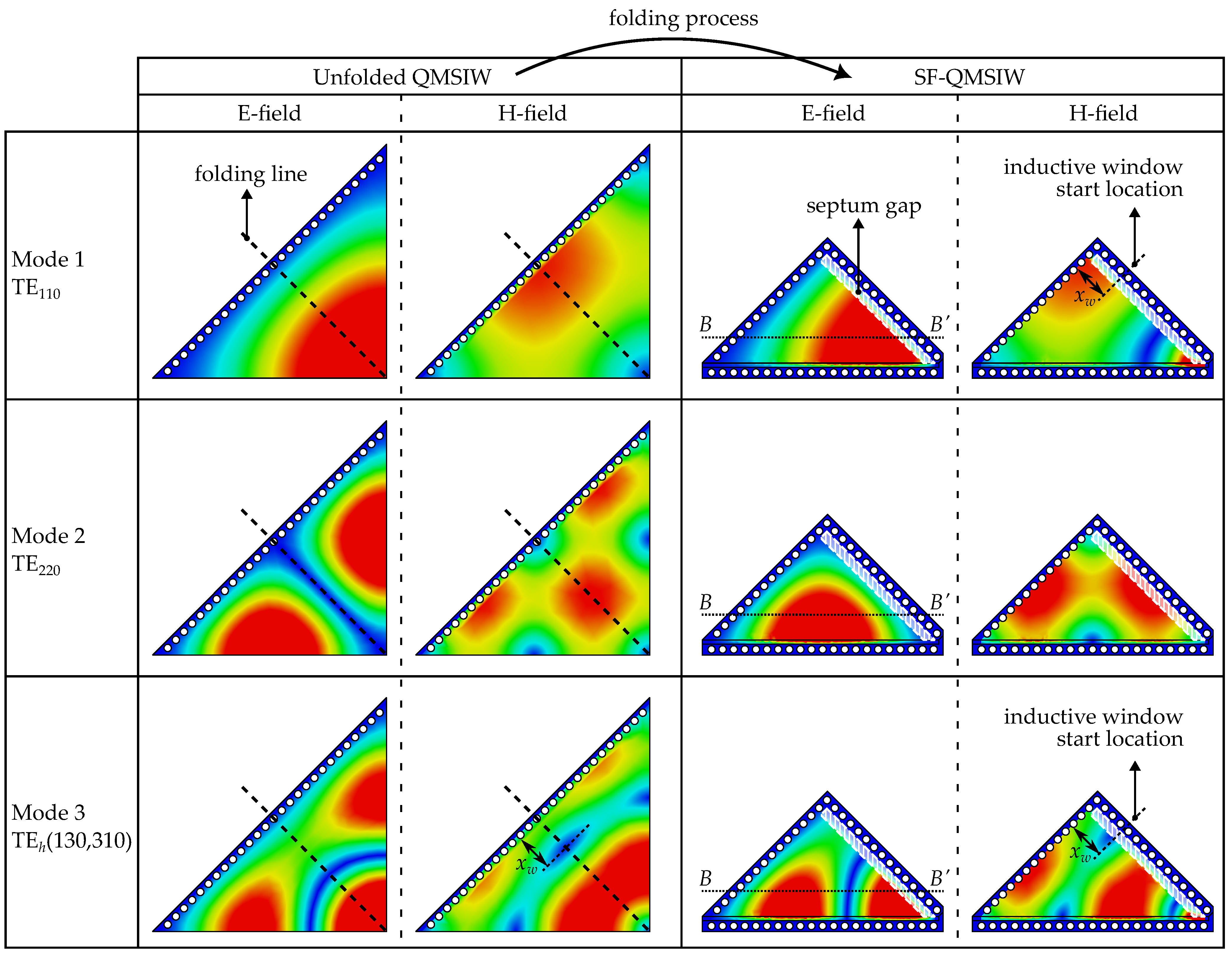
Figure 2 provides an overview of the simulated electric field (E-field) and magnetic field (H-field) distributions of the first three resonant cavity modes for both the unfolded conventional QMSIW (Figure 1b) and the SF-QMSIW cavity (Figure 1d). The plotted profiles (denoted as Mode 1, Mode 2, and Mode 3, respectively) are the TE 110 , TE 220 , and TE h ( 130 , 310 ) modes. The latter mode is the hybrid combination of the TE 130 and TE 310 modes [62,63]. In Figure 2, the folding line and septum gap are indicated by a bold dashed line and a white hatched pattern, respectively. The electric mode profiles for the SF-QMSIW show that the guard trace’s importance is in containing the fields within the cavity, since they are very strong near the open side. In an unshielded QMSIW or F-QMSIW structure (Figure 1b and Figure 1c, respectively), leakage of fields from this side would result in antenna-like operation and hence large radiation losses. Comparing the mode profiles between the unfolded QMSIW and SF-QMSIW (on the left and right side of Figure 2, respectively), both the electric and magnetic field distributions are very similar. However, the magnetic field strength is higher in the folded structures’ bottom right corner than in the unfolded counterparts. This can be attributed to the effects of the fringing fields in the region of the septum gap and guard trace.
In Figure 3, the simulated electric fields are displayed within the cross-section along B B for the SF-QMSIW structures (see the right side of Figure 2). The region of the septum gap is indicated by the dashed rectangles on the right side of the subfigures. Notice that the electric fields in this region are much stronger for Mode 1 and Mode 3 (Figure 3a and Figure 3c, respectively) than for Mode 2 (Figure 3b). This is because the structure’s folding line is located in the region of maximal E-field for Mode 1 and Mode 3. In contrast, for Mode 2, it is situated exactly in the region where the E-field is minimal (Figure 2). As a result, altering the septum gap width g s will have a more pronounced effect on the resonant frequency of the former two modes than it will have on that of Mode 2.

3. Dual-Band Bandpass Filter

In this section, the design of the proposed dual-band BPF is discussed. First, the design requirements are stipulated. Afterwards, the topology is presented, and the fabrication is explained. Finally, the adopted design methodology is illustrated by means of a flowchart.

3.1. Design Requirements

The proposed BPF is designed according to the following requirements, which are imposed by the application scenario of autonomous cars. First, to enable inconspicuous integration into the car’s dashboard, the filter should exhibit a low-profile structure and a small form factor. It should also be compatible with standard PCB manufacturing technology, both to reduce the fabrication costs and to enable straightforward co-integration with active electronics or other RF components.
Second, the filter should operate in a proper set of frequency bands that are relevant for vehicular communications. Vehicle-to-everything (V2X) entails all types of communication between the autonomous vehicle itself and the entities surrounding it. This includes vehicle-to-vehicle (V2V), vehicle-to-device (V2D), vehicle-to-pedestrian (V2P), and even vehicle-to-infrastructure (V2I) [64]. Up to this point, two primary technologies have been developed to enable V2X communications, which are based on either dedicated short-range communications (DSRCs) or cellular network connections [65]. DSRCs operate in a part of the Unlicensed National Information Infrastructure (U-NII) frequency bands, more specifically in the 5.9 GHz U-NII-4 band (5.850–5.925 GHz). For cellular technology, the 3.5 GHz 5G New Radio (NR) band (3.55–3.70 GHz) is frequently used. To support both technologies, as well as to accommodate connectivity in the popular 5.8 GHz industrial, scientific, and medical (ISM) band (5.725–5.875 GHz), the filter should operate according to the following frequency standards: 5G NR n48 (3.55–3.70 GHz), U-NII-3 (5.725–5.850 GHz), and U-NII-4 (5.850–5.925 GHz).
Third, a good filter characteristic is desired, exhibiting a low group delay variation and good selectivity. Additionally, to suppress unwanted interference from other frequency bands, excellent inter-band rejection between the lower and upper passband is required.

3.2. Filter Topology and Implementation

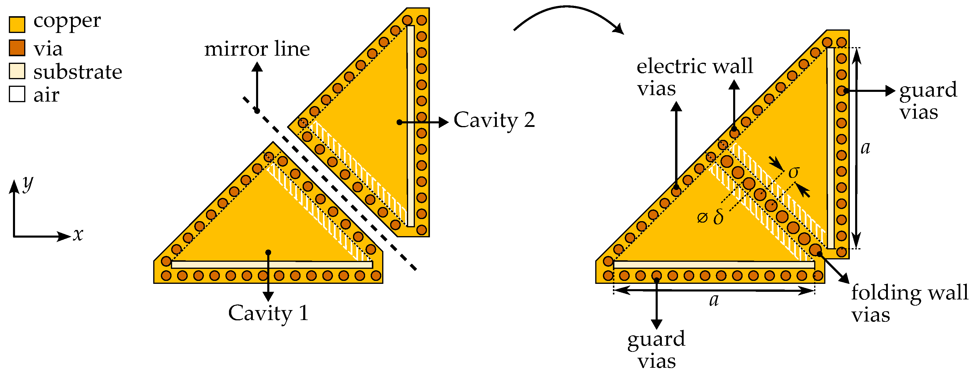
Figure 4 shows how the proposed filter topology is composed from the SF-QMSIW building block as described in Section 2. Two identical SF-QMSIW cavities, one of which is mirrored along the dashed mirror line, are placed back-to-back. Because their dimensions are identical, the number of variables that needs to be optimized during the design process is strongly decreased. These two cavities, denoted in Figure 4 as Cavity 1 and Cavity 2, are separated by a row of metallic vias with diameter δ and spacing σ . These via rows constitute the shared folding wall for both cavities. Furthermore, the cavities are shielded by electric wall vias and guard vias, as indicated in Figure 4.
The exploded view for the final topology of the proposed dual-band BPF is visualized in Figure 5. The filter is constructed as a stacked configuration of two dual-layer PCBs. These are held together by brass nuts and bolts with a diameter of 1 mm. The PCBs are implemented on an RO3003 high-frequency (HF) laminate with a relative permittivity ε r = 3 , a loss tangent tan δ = 0.001 , and a substrate thickness h = 0.508   mm . The metal layers, which are denoted by M1, M2, M3, and M4, are plated with a final copper thickness t = 35   μ m . Hence, the total thickness of the stacked filter structure is T = 2 h + 4 t = 1.156   mm . For enhanced visualization, the metal layers in Figure 5 are semitransparent. Furthermore, only a selection of nuts and bolts is drawn, and the grounding vias are not shown.
As indicated by the circled regions in Figure 5, the inter-resonator coupling between Cavity 1 and Cavity 2 is realized by opening an inductive coupling window in the folding wall. At this location, the septum gaps are closed. Moreover, a CPW coupling trace is implemented by etching two rectangular slots in the middle metal layers M2 and M3. The dimensions of the inductive coupling window and the CPW coupling trace are further discussed below. Furthermore, their coupling mechanisms, which target the coupling for the lower and upper passband, respectively, are thoroughly explained in Section 3.3.
Figure 6 shows each metal layer from Figure 5, namely, M1, M2, M3, and M4, in more detail (in Figure 6a, Figure 6b, Figure 6c, and Figure 6d, respectively). Also, in contrast to Figure 5, the grounding vias are now displayed. For several parts, indicated by Detail A, Detail B, and Detail C, a more detailed subfigure is provided (Figure 6e, Figure 6f, and Figure 6g, respectively). The width of the inductive coupling window is w w (Figure 6a). It is positioned at an offset o w from the electric wall vias (Figure 6c). Hence, its center is located at c w = o w + w w / 2 from those vias (Figure 6d). The region of the inductive coupling window in layers M2 and M3 is visualized more clearly in Detail B (Figure 6f). Notice that the separation between the cavities is controlled by the diameter δ of the folding wall vias, as well as by the window depth d s g . The latter is defined as the distance between the septum gaps of both cavities. The CPW coupling trace is located exactly at the window’s center. It consists of two identical slots with length l t and width w t , which are separated by distance s t .
To minimize radiation loss and to improve signal isolation, the cavities are fed by grounded coplanar waveguide (GCPW) feed lines. As discussed in more detail in Section 3.3, those feed lines are located on opposite metal layers, i.e., on M1 (Figure 6a) and M4 (Figure 6d), to generate additional TZs. The ground plane formed by M2 and M3 provides effective shielding between both lines. This, in turn, enhances the input/output (I/O) signal isolation. As indicated in Figure 6a,c, the feed lines enter the cavities at an offset o f from the cavity’s bisector. Negative values for the feed offset ( o f < 0 ) result in the feeds shifting towards the outer corners of the cavities (i.e., away from the folding wall), whereas positive values ( o f > 0 ) move both feeds towards each other and to the folding wall. A more detailed visualization of the feed line entering Cavity 2 on metal layer M1 is given in Figure 6e. The GCPW feed has a signal trace width w f 2 and a gap g f 2 between the signal trace and both coplanar ground planes. In the region of the guard gap g g , the width of the signal trace is tapered to w f 1 . For matching purposes, insets with length l i and width w i are provided where the feed enters the cavity. To maintain the structure’s compactness while providing enough space for the ESRR sections, the feed lines exhibit a 90° bend with a radius of curvature r. This allows them to be extended parallel to the cavities’ guard walls. The electric wall vias and guard vias have diameter d and spacing s. Additionally, multiple metallic grounding vias with the same diameter d are added around the feed lines. These vias provide a stable ground connection and suppress surface waves. Drilled holes with diameter d b = 1.00   mm are provided for the brass bolts.
In the signal trace of both GCPW feed lines, a pair of cascaded ESRRs is embedded (Detail C in Figure 6g). These ESRR sections provide second-mode suppression while minimizing their influence on the rest of the frequency range, as further explained in Section 3.3.3. Each of the ESRRs is constructed by removing a slot with length l s l and width w s l from the original signal trace. Then, the embedded resonator with length l r and width w r is symmetrically inserted into this slot. Both of its ends are shorted by a metallic via with diameter d r . Finally, small gaps g c are etched, creating an IDC structure with three fingers. Both ESRRs are separated by the distance s r . The first slot is etched at the distance o r from the PCB edge (Figure 6a).

3.3. Design Methodology

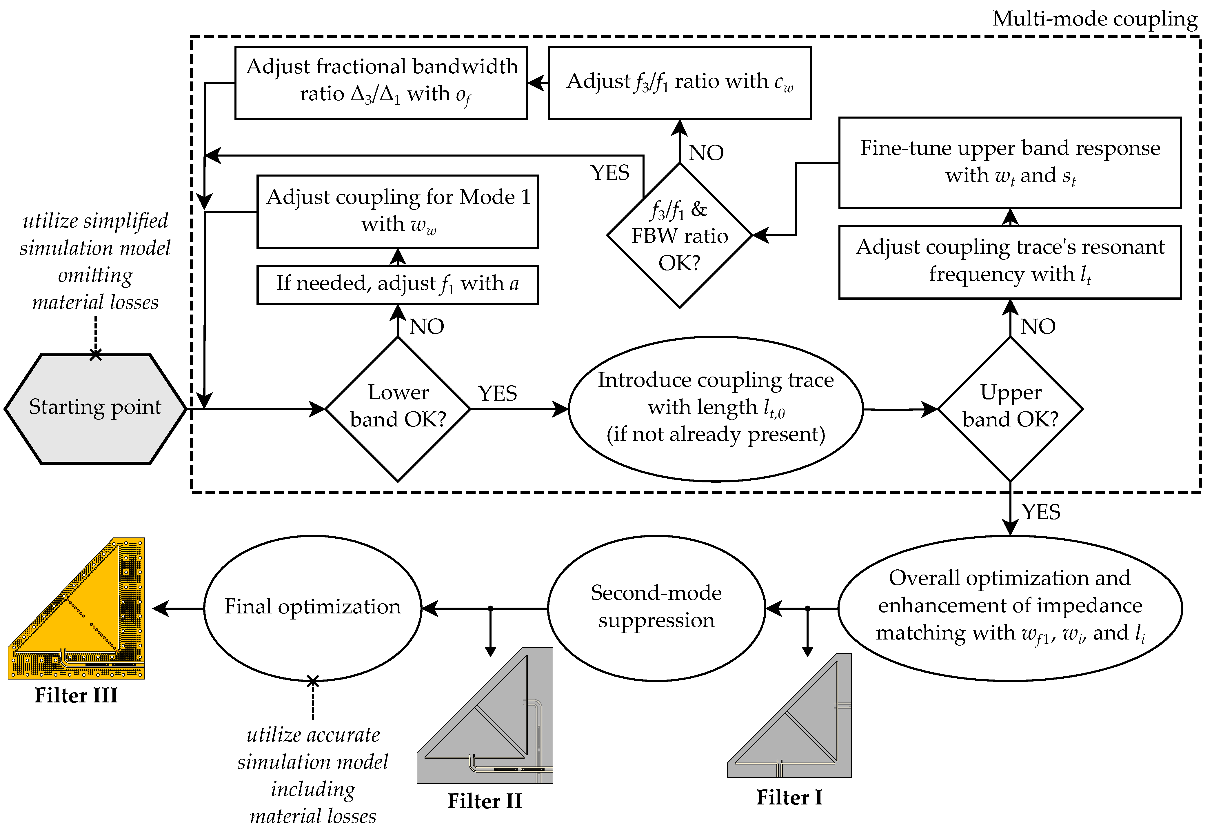
In this section, the design methodology is discussed according to the flowchart displayed in Figure 7. The individual steps are further explained below. Since the SF-QMSIW cavities are strongly perturbed by the CPW coupling trace, it is difficult to accurately extract the coupling coefficients and Q-factors. Therefore, rather than using conventional filter design methods, which are based on coupling theory and require the calculation of filter coefficients, the filter is designed and optimized using parametric analysis. All simulations are performed with the full-wave frequency domain (FD) solver of CST Studio Suite 2022.
Only the first and third modes of the SF-QMSIW cavity (Modes 1 and 3 in Figure 2) are exploited to construct the response for the lower and upper passband, respectively. The second mode (Mode 2 in Figure 2) is avoided since the maximal strength of its E-field occurs entirely at the cavity’s open side. Hence, utilizing this mode would result in larger radiation losses than for the other modes. Therefore, as further explained in Section 3.3.3, Mode 2 is suppressed.

3.3.1. Starting Point

Due to the iterative nature of the design process, time-consuming full-wave electromagnetic simulations should be avoided as much as possible. Therefore, as depicted in the first step of Figure 7, a simplified simulation model is adopted as a starting point, trading off accuracy for simulation speed. In this simplified simulation model, material losses are omitted. In addition, the via rows are replaced by solid sheets of perfect electric conductor (PEC). As a last step, a more accurate simulation model is adopted, and material losses are included. A final optimization is carried out using this accurate simulation model, resulting in the optimized dimensions of Filter III, as given in Table 1 of Section 4.1.
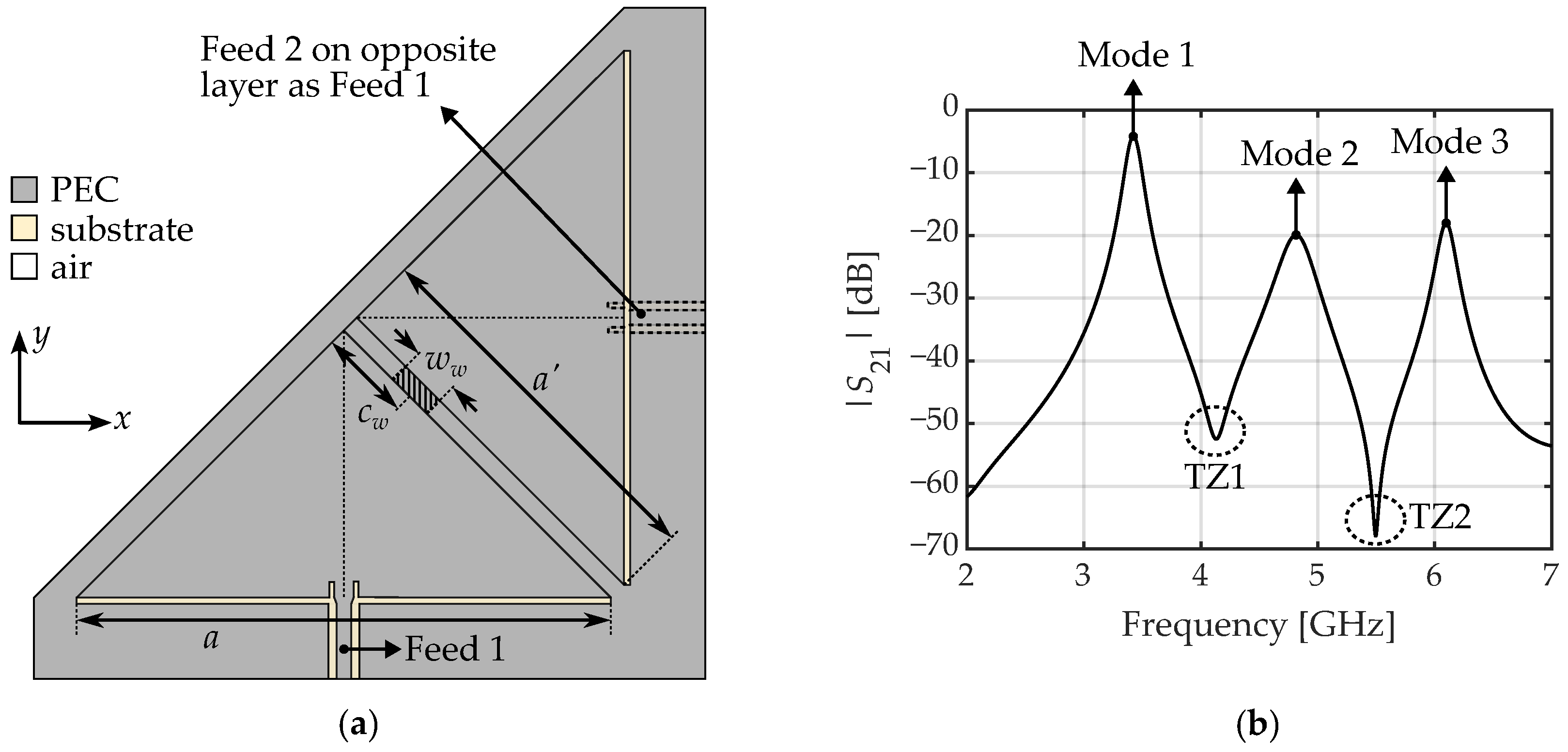
The starting topology is shown in Figure 8a. It is idealized as described above. Moreover, it does not yet feature the bent feed lines with ESRR sections. Initially, a starting point for the SF-QMSIW cavity dimension a is calculated using Equation (1) for the fundamental resonant frequency f 110 of its square unfolded counterpart. Afterwards, a is adapted such that the resonant frequency of Mode 1 (Figure 8b) is close to the desired lower frequency band, namely, 5G NR n48 (3.55–3.70 GHz), as described in Section 3.1.
As shown in Figure 8a, the feed lines are located on opposite metal layers (i.e., Feed 1 on M1 and Feed 2 on M4, or vice versa). This configuration is chosen because it generates two additional TZs (circled in Figure 8b): one between Mode 1 and Mode 2 (TZ1), and one between Mode 2 and Mode 3 (TZ2). These TZs appear due to destructive interference between multiple signal paths that exist between the input and output ports [12,66,67].
Figure 9 shows the influence of the feed offset o f on both the starting topology’s transmission characteristic (Figure 9a) and the external quality factor of each mode (Figure 9b). The latter is extracted from the simulated group delay of S 11 for a single SF-QMSIW resonator (i.e., with Cavity 2 removed and the inductive coupling window closed), using the following [68]:
Q e = 2 π f 0 τ ( f 0 ) 4 .
In the equation above, f 0 is the resonant frequency of each mode, derived from the peak of the group delay, and τ ( f 0 ) represents the corresponding peak group delay value. The external quality factors for Mode 1, Mode 2, and Mode 3 are denoted by Q e I , Q e II , and Q e III , respectively. For increasing feed offset (i.e., for the feeds moving towards each other, as explained in Section 3.2), the third mode’s Q-factor increases, and that of the first mode decreases (and vice versa). Since the 3 dB bandwidth Δ f 3 dB of a resonant mode is related to its Q-factor according to [68]:
Q e = f 0 Δ f 3 dB ,
this relationship implies that the fractional bandwidth (FBW) ratio Δ = Δ 3 / Δ 1 (with Δ 3 and Δ 1 being the FBWs of the passbands composed by Mode 3 and Mode 1, respectively) is controlled by the feed offset. Initially, the feed offset is chosen as o f = 0 : the feeds are centered on the cavity’s triangular bisector (dashed line in Figure 8a). This value is then iteratively adjusted during the design process to implement the required FBW ratio (Figure 7).
Initially, the center of the inductive coupling window c w (Figure 8a) is located where the H-field for Mode 3 is minimal (Figure 2), i.e., c w = x w = a / 4 = a / ( 4 2 ) . At this location, the H-field for Mode 1 is strong (Figure 2). Hence, in the start position, the inductive coupling window can be primarily used to control the coupling for Mode 1, while exerting a minimal effect on Mode 3.

3.3.2. Multimode Coupling

This section discusses the multimode coupling mechanisms between the two cavities, as well as the optimization of the lower and upper passband responses (dashed rectangle in Figure 7). First, the lower passband response is controlled by only exploiting the inter-resonator coupling provided by the inductive coupling window. Figure 10 shows the influence of the window width w w on both the filter’s transmission characteristic (Figure 10a) and the calculated coupling coefficient (Figure 10b). Since the window is strategically located in the region where the H-field is high for Mode 1 but low for Mode 3 (Figure 2), the window width primarily affects the coupling for the first mode. Hence, Figure 10 only shows the effect on this mode. The coupling coefficient k I for Mode 1 is calculated using the following [68]:
k I = f p 2 2 f p 1 2 f p 2 2 + f p 1 2 ,
with f p 1 and f p 2 representing the frequency of the lower and upper resonance from the coupled Mode 1, respectively. As observed from Figure 10b, k I increases with increasing values of w w . The increased coupling results in the mode bifurcation observed in Figure 10a. In this stage of the design process, a suitable window width is selected such that sufficient coupling for Mode 1 and the desired bandwidth for the lower passband are achieved. Additionally, if the center frequency f 1 for this passband needs adjustment, it can be fine-tuned by slightly altering the cavity dimension a.
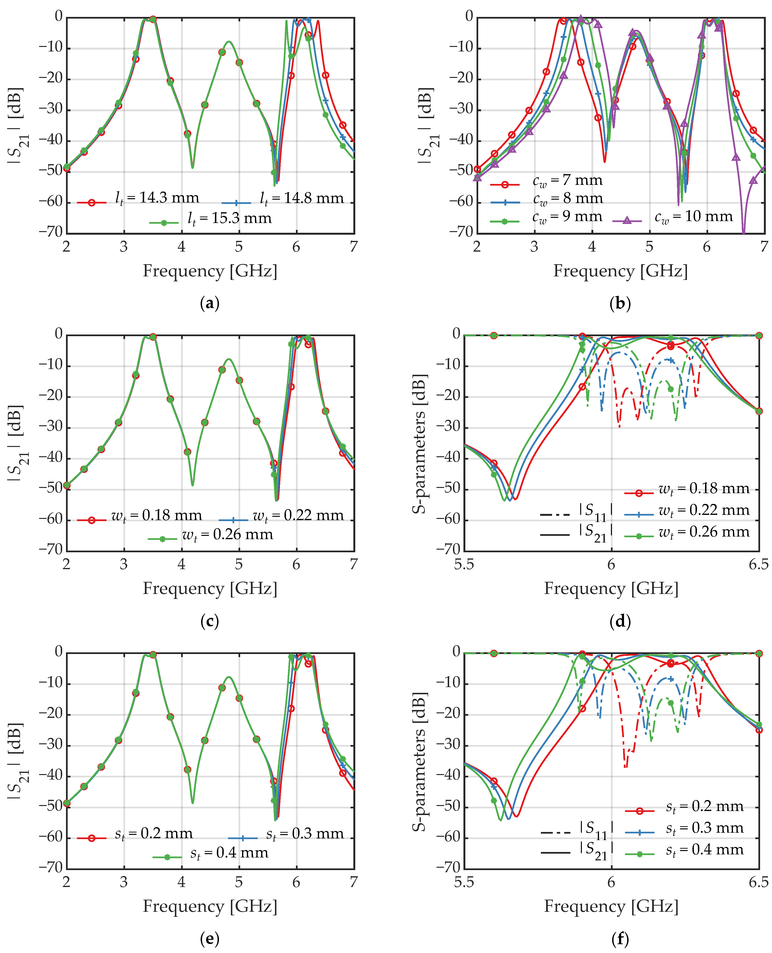
Second, the upper passband response is optimized. This is done by inserting a CPW coupling trace through the center of the window. This trace is formed by two rectangular shorted slots with length l t , width w t , and separation s t (Figure 6f). The purpose of the coupling trace is threefold. First and foremost, it acts as a CPW half-wavelength resonator with resonant frequency f t . The relationship between f t and l t is given by the following:
f t = c 2 l t ε r .
By appropriately selecting the initial trace length l t , 0 , the frequency f t is positioned near the resonant frequency of Mode 3. Thereby, it extends the upper passband’s bandwidth. As a second function, the coupling trace provides electric coupling for Mode 3, as it connects the regions of the maximal E-field for this mode (Figure 2). Hence, it allows for controlling the coupling for the upper passband. Finally, the coupling trace serves as a mechanism to control the f 3 / f 1 ratio. Here, f 1 and f 3 correspond to the center frequencies of the passbands constituted by Mode 1 and Mode 3, respectively. Each of these effects is illustrated below.
Figure 11 presents a parametric analysis for various parameters related to the coupling trace. As shown in Figure 11a, the coupling trace length l t determines the resonant frequency of the CPW resonator. Hence, l t is chosen to fix this resonant frequency near Mode 3 such that an extended bandwidth is achieved. Figure 11b shows the influence of the inductive window’s center position c w on the f 3 / f 1 ratio. Since the coupling trace is located in the window’s center, increasing c w shifts the coupling trace towards the cavity’s inner corner. The coupling trace cuts the surface currents for Mode 1 and decreases the effective cavity size for this mode. In this manner, f 1 is pushed to higher frequencies, thereby decreasing the f 3 / f 1 ratio. Note that, due to the varying fields at different window positions (Figure 2), the coupling mechanisms for both passbands may slightly change when c w is altered. Therefore, both c w and w w have to be re-optimized iteratively during the design process. Nonetheless, the couplings for the lower and upper passband remain predominantly controlled by the inductive window and coupling trace, respectively. Figure 11c,d demonstrate the effect of the coupling trace’s slot width w t : this parameter only influences the mixed coupling for Mode 3, while leaving the other modes unaffected. A similar effect is displayed in Figure 11e,f. Both subfigures show the influence of the coupling trace’s slot separation s t . Consequently, both w t and s t can be used to fine-tune the upper passband response.
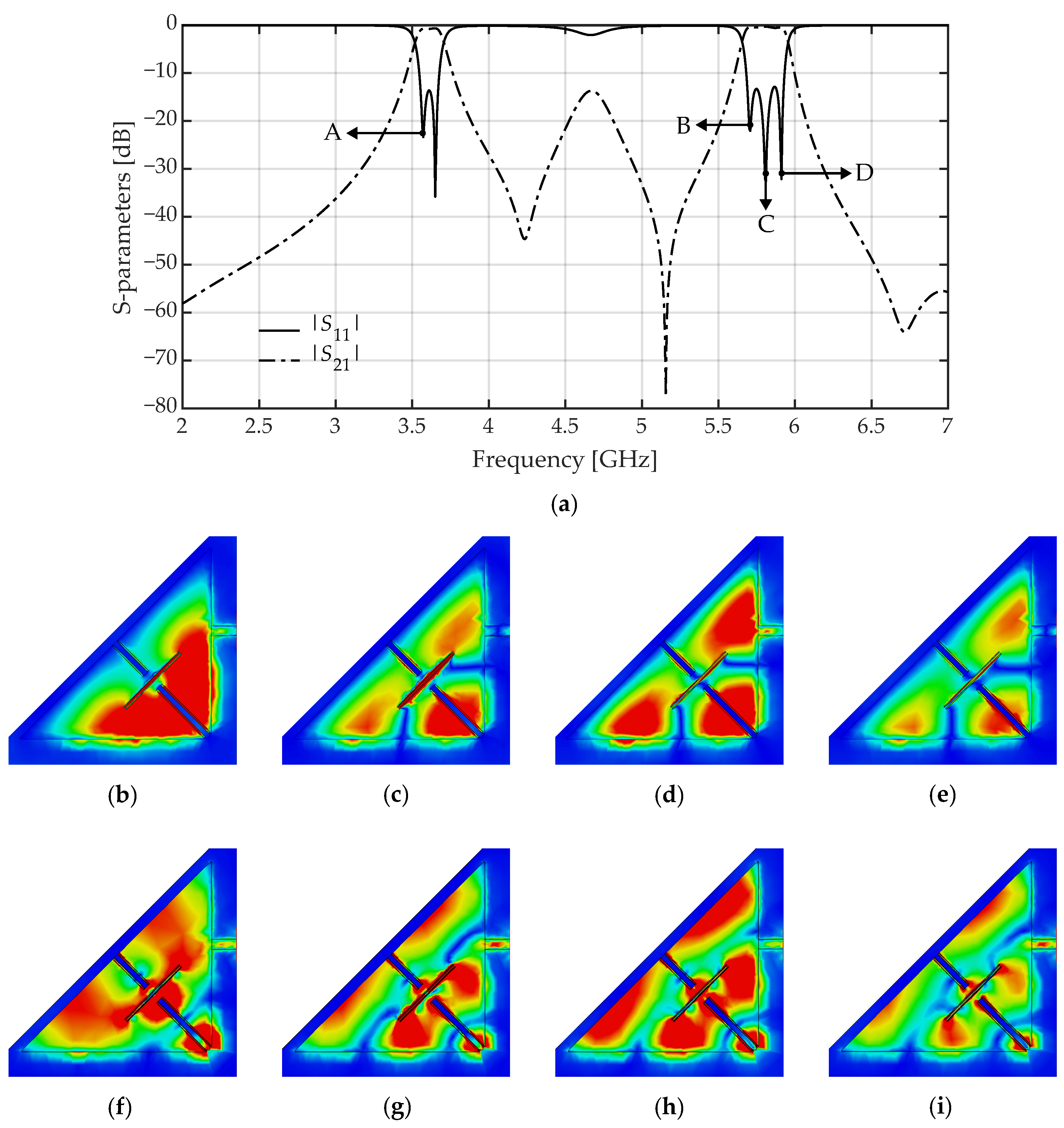
When the desired inter-resonator coupling and FBW ratio Δ between the lower and upper passband are achieved, the overall structure is optimized. Additionally, the impedance matching can be improved by adjusting the feed dimensions ( w f 1 , w i , and l i ). The result of this intermediate optimization process is Filter I (Figure 7), whose simulated S-parameters are given in Figure 12. Furthermore, the simulated E-fields and H-fields are shown in Figure 12b–e and Figure 12f–i, respectively. For the lower passband, only the fields at frequency point A are provided. The other resonance located in this band is very similar. Figure 12c shows the resonant behavior of the half-wavelength CPW resonator at frequency point B. In Figure 12b, one sees how the coupling trace perturbs the E-field of Mode 1, which results in the manipulation of the f 3 / f 1 ratio, as described above.

3.3.3. Second-Mode Suppression

As explained in Section 3.3.2, the lower and upper passbands are formed by exploiting Modes 1 and 3, respectively. In contrast, Mode 2 is unused by design, since its maximal E-field is concentrated at the SF-QMSIW cavity’s open side (Figure 2). However, this mode causes a transmission peak at 4.68 GHz. This effect is visible in the intermediate design result of Filter I and seen in Figure 12. To avoid potential interference from other frequency bands existing in this region, such as the C-band, the second mode needs to be suppressed.
To suppress the second mode, a small band notch filter based on ESRRs [56] is designed and integrated with Filter I. To provide the space required for this structure, the feed lines of Filter I are bent and extended, as illustrated in Figure 5 and Figure 6. In both feed lines, an identical section consisting of a pair of identical ESRR unit cells is embedded. The ESRR-based notch filter has the benefit that its design can be completely separated from the original BPF design procedure, as visualized in Figure 7. Furthermore, besides the extension of the feeds, no additional space is required since the ESRRs are entirely embedded in the structure’s feeding transmission lines (TMLs). In contrast to the ESRRs proposed in [56], no lumped components such as external capacitors or varactors are used. Instead, the required capacitance is realized using an integrated IDC structure. This simplifies the filter implementation and grants the designer more precise control.
Figure 6g shows the structure of the ESRR section. The slot width w s l is fixed such that the defected TML does not result in a discontinuity of the line’s characteristic impedance [56]. An embedded resonator is inserted in this slot, with the width w r chosen so that there is enough space for an IDC structure with three fingers. Both the width w c of the IDC’s fingers and the gap g c between them are equal to 100 μm, as they are constrained by the technological limitations of the PCB manufacturing process. The notch frequency is mainly determined by the resonator’s length l r and by the capacitance provided by the IDC, which is controlled by the finger length l c . To create a sharper notch and minimize the influence on the BPF passband frequencies, two ESRR unit cells are cascaded.
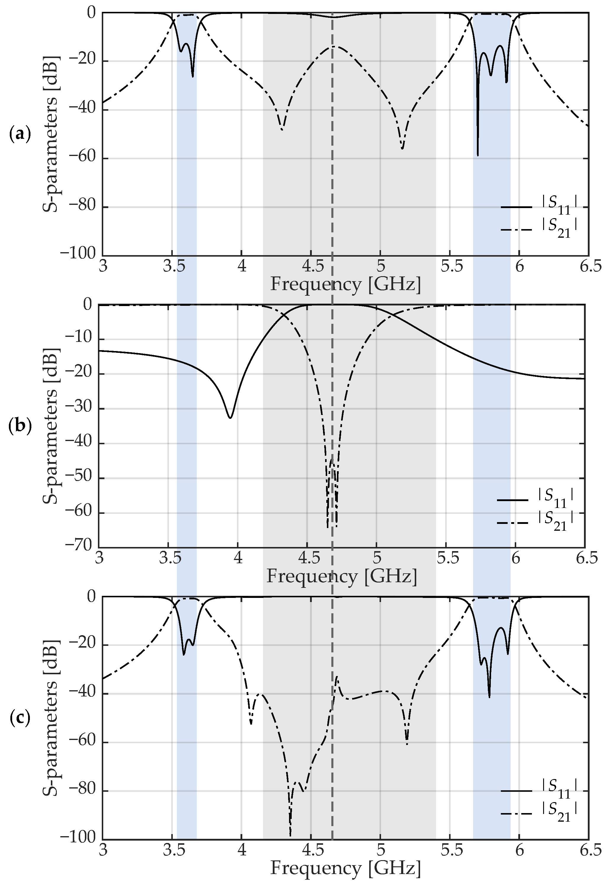
The design procedure for the ESRR-loaded BPF is illustrated in Figure 13. First, the ESRR section is designed separately as a stand-alone component, with a notch frequency located exactly at the BPF’s second-mode resonant frequency, namely, at 4.68 GHz (Figure 13b). Afterwards, it is embedded into the extended feed lines of the unloaded BPF (Figure 13a), resulting in the characteristic of Filter II (Figure 7), which is shown in Figure 13c. By fine-tuning the ESRR separation s r and the offset o r , an optimized response is achieved.
The gray area in Figure 13 indicates the region where the simulated reflection coefficient | S 11 | of the stand-alone ESRR section remains above 10 dB. Hence, outside this region, the ESRR’s effect on the original filter characteristic will be minimal. This is seen by comparing the lower and upper passbands before and after application of the ESRR section (indicated by the blue areas in Figure 13). It demonstrates the excellent potential for the ESRR to be designed completely separately from the rest of the filter component.

4. Experimental Results and Discussion

In this section, a prototype is realized and experimentally verified. First, the prototype’s dimensions are given, and practical measures to increase the filter’s robustness are described. Next, the measurement results are presented and discussed.

4.1. Optimized Dimensions and Fabrication Aspects

After the design process described in Section 3.3, a more realistic simulation model with lossy materials is adopted. In this model, the electric walls are replaced by metallic via rows. Then, a final optimization is carried out, resulting in Filter III in Figure 7 (and shown in the topology of Figure 5 and Figure 6). The final dimensions of this filter are listed in Table 1.
Figure 14 shows photographs of the fabricated and fully assembled prototype. The overall structure’s surface area is 0.71 λ g 2 , with λ g being the guided wavelength in the dielectric at the lower passband’s center frequency. SubMiniature version A (SMA) connectors are soldered to the GCPW feed lines. To increase the filter’s robustness, several precautionary measures are taken. First, to prevent air gaps between the PCBs, three folding wall vias are replaced by brass bolts. Therefore, at the position of those vias, holes are drilled with a diameter equal to d b . Second, to prevent misalignment issues, the width of the septum gaps g s and the coupling trace slots w t are slightly enlarged on metal layer M3 compared to the nominal values on metal layer M2 (as listed in Table 1). Lastly, the coupling trace length is extended by 100 μm with respect to the nominal value l t mentioned in Table 1. This measure is taken to compensate for the effect where sharp corners are rounded in the PCB manufacturing process. This results in a coupling trace that appears slightly shorter.
Table 1. Final dimensions of the proposed dual-band BPF (refer to Figure 6).
ParameterValue [mm]ParameterValue [mm]ParameterValue [mm]ParameterValue [mm]
a35.31 w w 3.20 w i 0.30 w r 0.50
d0.35 l t 15.52 l i 1.00 l r 6.95
s0.70 w t 0.19 w f 1 1.27 l r 7.75
δ 0.80 s t 0.26 o f 1.00 * d r 0.30
σ 1.30 e 1 9.00 w f 2 1.00 s r 1.20
d b 1.00 e 2 3.00 g f 2 0.50 o r 3.10
d s g 1.20 d f 2 3.00r2.00 w c 0.10
c w 10.30 g s 0.31 w s l 0.80 l c 6.05
o w 8.70 g g 0.40 l s l 8.25 g c 0.10
* Refer to Section 3.2 for the meaning of the negative sign with of.

4.2. Measurement Results

The assembled filter prototype is experimentally validated by conducting a full two-port S-parameter measurement using a Keysight N5242B PNA-X vector network analyzer (VNA). The S-parameters are measured with respect to a reference impedance of 50 Ω .
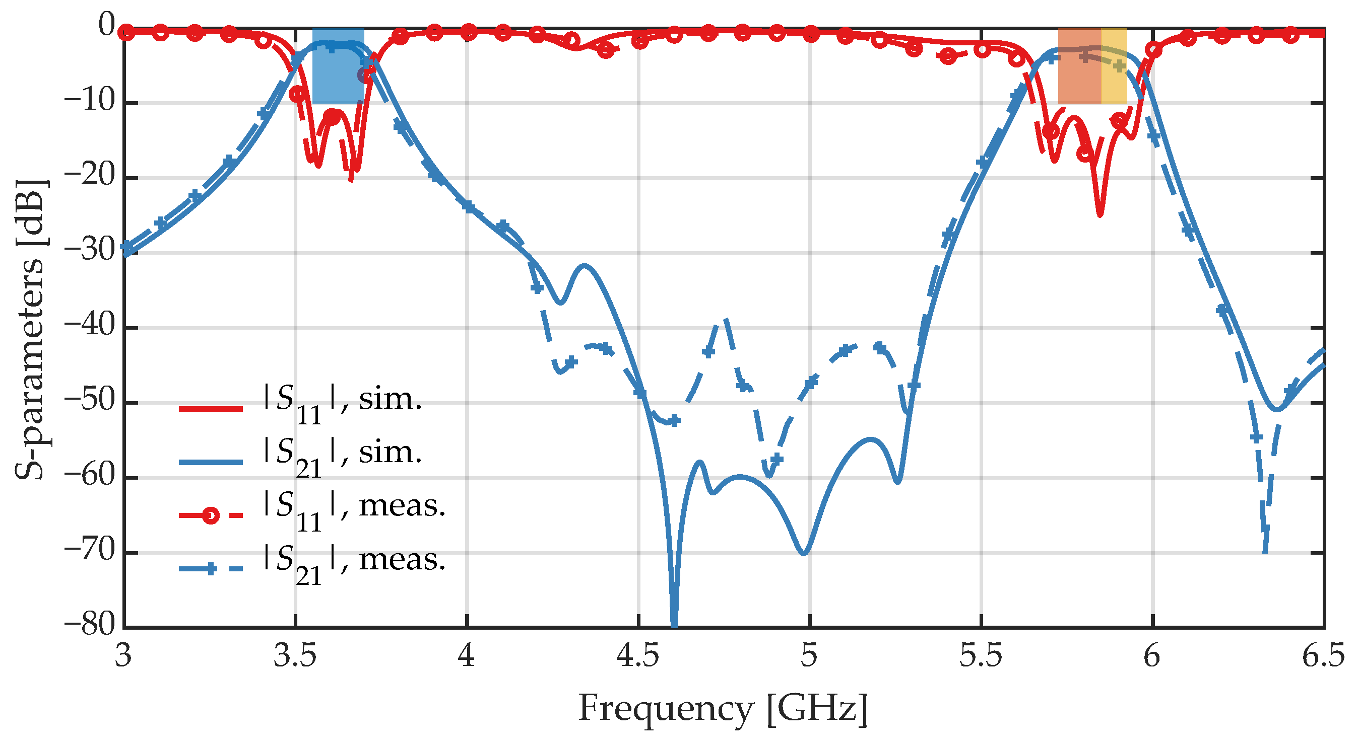
Figure 15 compares the simulated and measured S-parameters. These are indicated by solid and dashed lines, respectively. The reflection coefficient | S 11 | is shown in red and the transmission coefficient | S 21 | in blue. Furthermore, the desired frequency bands of operation, as listed in Section 3.1, are indicated by blue (5G NR n48), orange (U-NII-3), and yellow (U-NII-4) rectangles. Overall, excellent agreement between simulation and measurement is observed. However, the measured insertion loss (IL) in the upper passband is a bit higher than simulated. The two passbands have a measured center frequency of 3.6 GHz and 5.8 GHz. They exhibit a measured 3 dB FBW of 6.4% and 5.3%, respectively. Furthermore, the measured (and simulated) minimum ILs in both bands equal 2.37 dB ( 1.95 dB) and 3.74 dB ( 2.60 dB), respectively. Since the dimensions of the CPW coupling trace are critical for the upper passband performance, small deviations in these dimensions result in slightly more discrepancies at higher frequencies than observed at lower frequencies.
Figure 15 shows that, due to the effective second higher-order mode suppression, the measured inter-band rejection remains better than 38 dB over the wide frequency range from 1.17 f 1 to 1.48 f 1 , with f 1 being the center frequency of the lower passband. A highly selective filter characteristic is achieved, with roll-off rates of 50 dB/GHz and 56 dB/GHz at the lower passband’s lower and upper side, respectively, and 130 dB/GHz and 171 dB/GHz at the upper passband’s lower and upper side, respectively.
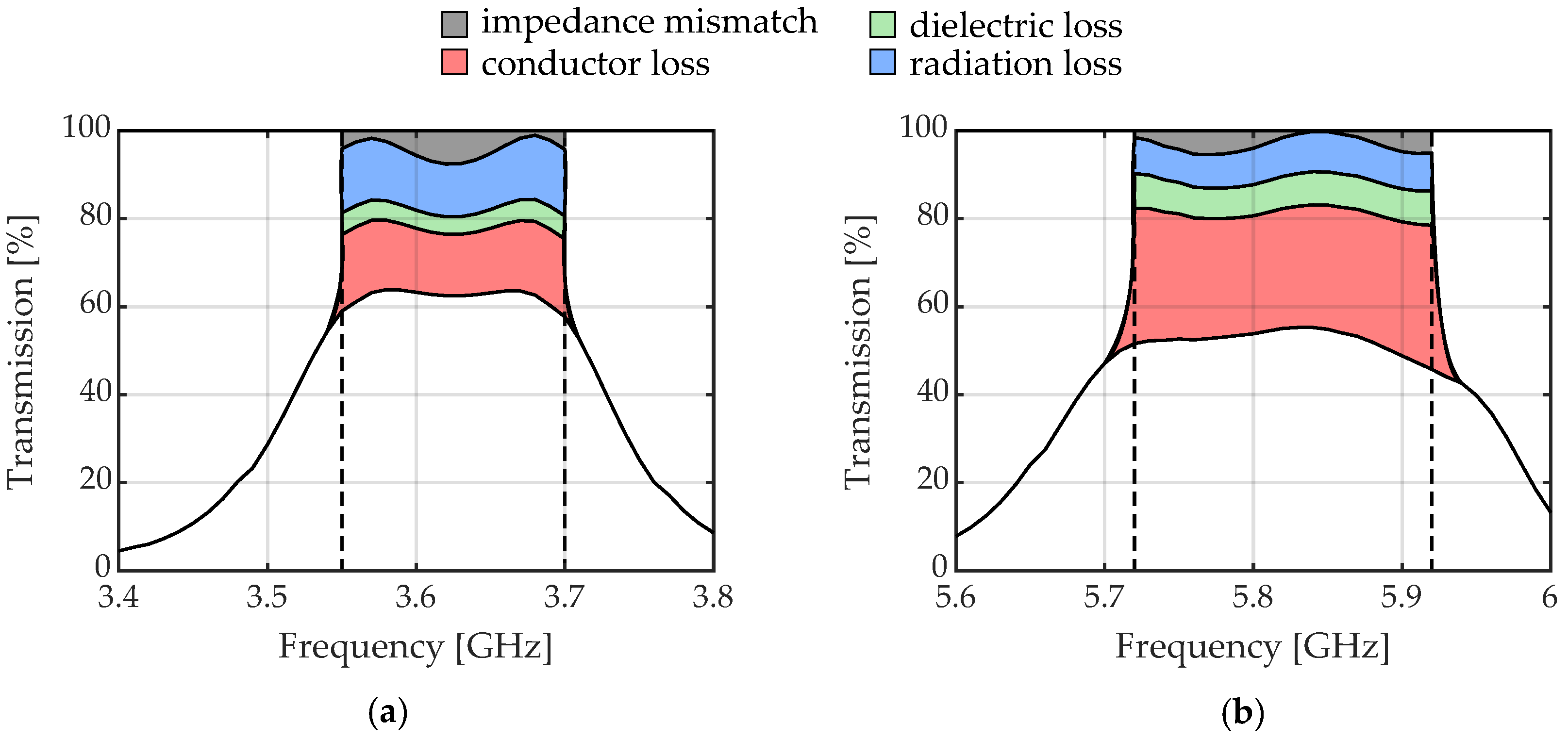
A detailed overview of the loss mechanisms contributing to the simulated IL is provided in Figure 16. Since much of the design process is performed using a simplified simulation model that omits material losses (as explained in Section 3.3.1), this figure also helps to clarify the difference between the simulated ILs in Figure 12, Figure 13 and Figure 15: for Filter I and Filter II, only radiation losses are taken into account, whereas for Filter III, also conductor and dielectric losses are considered. As observed by comparing Figure 16a,b, the higher IL in the upper passband results from the higher-order mode’s increased dielectric and copper losses, mostly originating from the CPW coupling trace and the ESRRs. Nonetheless, radiation losses remain low, owing to the filter’s shielded topology and the low radiation loss contributed by the ESRR sections (as simulated in Figure 13).
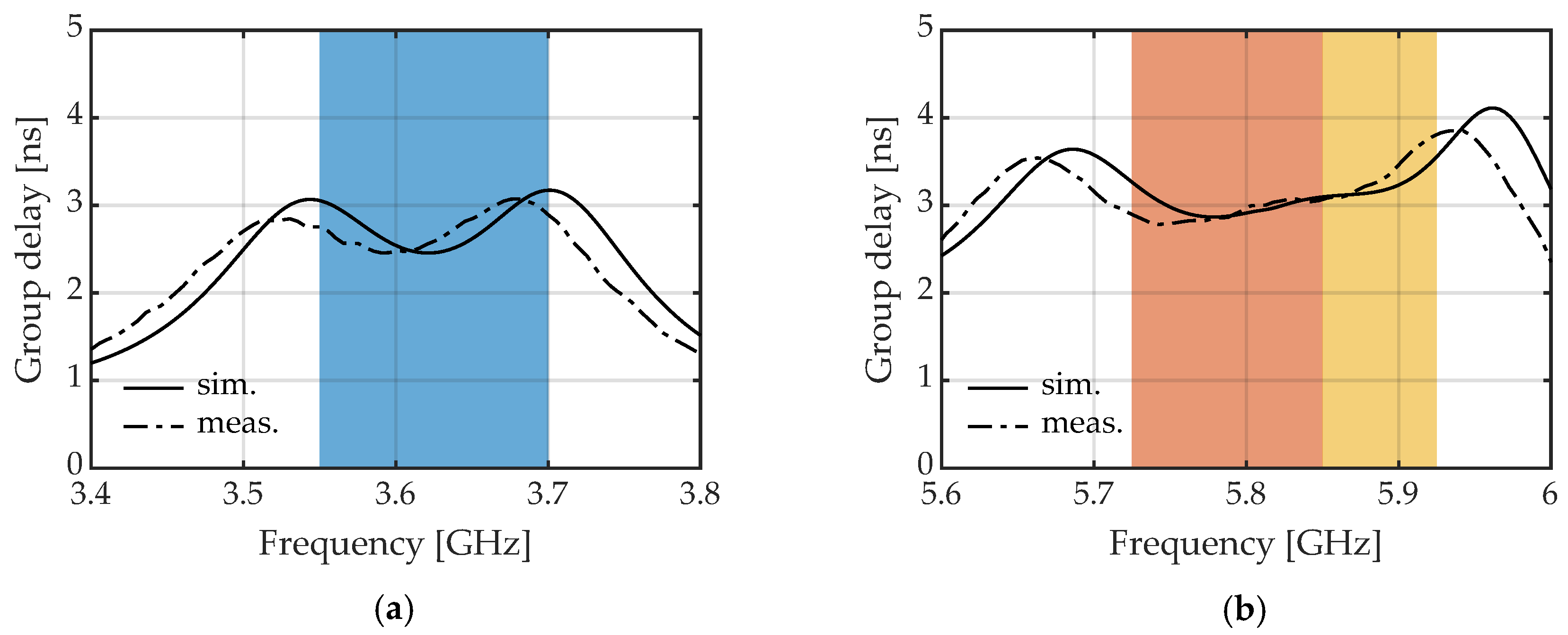
The measured and simulated group delays are shown in Figure 17. Similar to Figure 15, the 5G NR n48, U-NII-3, and U-NII-4 frequency bands are indicated by blue, orange, and yellow rectangles, respectively. Very good agreement between simulation and measurement is also observed here. Moreover, the measured in-band group delay variation is extremely low, exhibiting values of only 0.62 ns and 1.00 ns for the lower and upper passband, respectively. This is important because a low group delay ripple in the passband suggests that the filter maintains excellent linearity across different frequencies [69].
Table 2 provides a comparison with some dual-band BPFs reported in the recent literature. This comparison focuses on SIW-based filters that combine hybrid and MMR-based design strategies. Observe that the filter proposed in this paper is the first one that leverages hybrid technology in a folded SIW structure. Moreover, it provides best-in-class inter-band rejection within a reasonably compact footprint.

5. Conclusions

We have proposed a novel dual-band BPF based on shielded and folded QMSIW multimode cavities. Combining the merits of hybrid and MMR-based design strategies with a folded structure, this topology offers great design flexibility within a compact footprint. Additionally, by incorporating IDC-structured ESRR elements into the GCPW feed lines, suppression of the second higher-order mode is achieved. This results in excellent inter-band rejection. The proposed filter has been fabricated, and its effectiveness has been experimentally validated, showing low group delay variation and steep roll-off rates. It is particularly well-suited for next-generation IoT applications, such as the in-dashboard integration of wireless systems within self-driving cars, for several reasons. First, it supports a diverse combination of cellular and non-cellular as well as licensed and unlicensed frequency bands, namely, 5G NR n48 (3.55–3.70 GHz), U-NII-3 (5.725–5.850 GHz), U-NII-4 (5.850–5.925 GHz), and 5.8 GHz ISM (5.725–5.875 GHz). These bands are specifically useful for V2X communications. Second, the filter’s superior inter-band rejection ensures reliable operation in the presence of out-of-band electromagnetic interference. Finally, its compact size and compatibility with standard PCB manufacturing processes facilitate seamless integration and cost-effective mass production.

Author Contributions

Conceptualization, N.C., K.Y.K., J.V. and H.R.; methodology, N.C., K.Y.K., J.V. and H.R.; software, N.C.; validation, N.C.; formal analysis, N.C.; investigation, N.C.; resources, J.V. and H.R.; data curation, N.C.; writing—original draft preparation, N.C.; writing—review and editing, K.Y.K., J.V. and H.R.; visualization, N.C.; supervision, J.V. and H.R.; project administration, J.V. and H.R.; funding acquisition, J.V. and H.R. All authors have read and agreed to the published version of the manuscript.

Funding

This research was supported in part by the Flemish Research Foundation (FWO), grant number SBO S001521N.

Data Availability Statement

The raw data supporting the conclusions of this article will be made available by the authors on request.

Conflicts of Interest

The authors declare no conflicts of interest. The funders had no role in the design of the study; in the collection, analyses, or interpretation of data; in the writing of the manuscript; or in the decision to publish the results.

References

  1. Al-Fuqaha, A.; Guizani, M.; Mohammadi, M.; Aledhari, M.; Ayyash, M. Internet of Things: A Survey on Enabling Technologies, Protocols, and Applications. IEEE Commun. Surv. Tutorials 2015, 17, 2347–2376. [Google Scholar] [CrossRef]
  2. Ejaz, W.; Anpalagan, A.; Imran, M.A.; Jo, M.; Naeem, M.; Qaisar, S.B.; Wang, W. Internet of Things (IoT) in 5G Wireless Communications. IEEE Access 2016, 4, 10310–10314. [Google Scholar] [CrossRef]
  3. Qadir, Z.; Le, K.N.; Saeed, N.; Munawar, H.S. Towards 6G Internet of Things: Recent Advances, Use Cases, and Open Challenges. ICT Express 2023, 9, 296–312. [Google Scholar] [CrossRef]
  4. Vaezi, M.; Azari, A.; Khosravirad, S.R.; Shirvanimoghaddam, M.; Azari, M.M.; Chasaki, D.; Popovski, P. Cellular, Wide-Area, and Non-Terrestrial IoT: A Survey on 5G Advances and the Road Toward 6G. IEEE Commun. Surv. Tutorials 2022, 24, 1117–1174. [Google Scholar] [CrossRef]
  5. Zhang, J.; Liu, Q.; Zhou, D.; Zhang, D. Single-and Triple-Band Bandpass Filters Using Novel Perturbed Isosceles Right-Angled Triangular SIW Cavities. IET Microwav. Antennas Propag. 2021, 15, 241–252. [Google Scholar] [CrossRef]
  6. Chu, P.; Hong, W.; Tuo, M.; Zheng, K.L.; Yang, W.W.; Xu, F.; Wu, K. Dual-Mode Substrate Integrated Waveguide Filter With Flexible Response. IEEE Trans. Microw. Theory Tech. 2016, 65, 824–830. [Google Scholar] [CrossRef]
  7. Basit, A.; Khattak, M.I.; Al-Hasan, M.; Nebhen, J.; Jan, A. Design and Analysis of a Compact GSM/GPS Dual-Band Bandpass Filter Using a T-Shaped Resonator. J. Electromagn. Eng. Sci. 2022, 22, 138–145. [Google Scholar] [CrossRef]
  8. Zhang, G.; Basit, A.; Khan, M.I.; Daraz, A.; Saqib, N.; Zubir, F. Multi Frequency Controllable In-Band Suppressions in a Broad Bandwidth Microstrip Filter Design for 5G Wi-Fi and Satellite Communication Systems Utilizing a Quad-Mode Stub-Loaded Resonator. Micromachines 2023, 14, 866. [Google Scholar] [CrossRef] [PubMed]
  9. Basit, A.; Daraz, A.; Khan, M.I.; Zubir, F.; AlQahtani, S.A.; Zhang, G. Design and Modelling of a Compact Triband Passband Filter for GPS, WiMAX, and Satellite Applications with Multiple Transmission Zero’s. Fractal Fract. 2023, 7, 511. [Google Scholar] [CrossRef]
  10. Nwajana, A.O.; Obi, E.R. A Review on SIW and Its Applications to Microwave Components. Electronics 2022, 11, 1160. [Google Scholar] [CrossRef]
  11. Li, P.; Chu, H.; Chen, R.S. Design of Compact Bandpass Filters Using Quarter-Mode and Eighth-Mode SIW Cavities. IEEE Trans. Components Packag. Manuf. Technol. 2017, 7, 956–963. [Google Scholar] [CrossRef]
  12. Azad, A.R.; Mohan, A. Single-and Dual-Band Bandpass Filters Using a Single Perturbed SIW Circular Cavity. IEEE Microw. Wirel. Components Lett. 2019, 29, 201–203. [Google Scholar] [CrossRef]
  13. Lai, Q.; Fumeaux, C.; Hong, W.; Vahldieck, R. Characterization of the Propagation Properties of the Half-Mode Substrate Integrated Waveguide. IEEE Trans. Microw. Theory Tech. 2009, 57, 1996–2004. [Google Scholar]
  14. Cheng, Y.; Hong, W.; Wu, K. Half Mode Substrate Integrated Waveguide (HMSIW) Directional Filter. IEEE Microw. Wirel. Components Lett. 2007, 17, 504–506. [Google Scholar] [CrossRef]
  15. Iqbal, A.; Tiang, J.J.; Lee, C.K.; Mallat, N.K.; Wong, S.W. Dual-Band Half Mode Substrate Integrated Waveguide Filter With Independently Tunable Bands. IEEE Trans. Circuits Syst. II Express Briefs 2019, 67, 285–289. [Google Scholar] [CrossRef]
  16. Weng, M.H.; Tsai, C.Y.; Chen, D.L.; Chung, Y.C.; Yang, R.Y. A Bandpass Filter Using Half Mode SIW Structure With Step Impedance Resonator. Electronics 2020, 10, 51. [Google Scholar] [CrossRef]
  17. Iqbal, A.; Jiat Tiang, J.; Kin Wong, S.; Alibakhshikenari, M.; Falcone, F.; Limiti, E. Multimode HMSIW-Based Bandpass Filter With Improved Selectivity for Fifth-Generation (5G) RF Front-Ends. Sensors 2020, 20, 7320. [Google Scholar] [CrossRef]
  18. Zhang, L.; Wu, A.; Zhang, P.; Zhang, Z. Triangular Cavity Multi-Passband HMSIW Filter Based on Odd-Even Mode Analysis. Electronics 2021, 10, 2927. [Google Scholar] [CrossRef]
  19. He, Z.; You, C.J.; Leng, S.; Li, X.; Huang, Y.M. Compact Bandpass Filter with High Selectivity Using Quarter-Mode Substrate Integrated Waveguide and Coplanar Waveguide. IEEE Microw. Wirel. Components Lett. 2017, 27, 809–811. [Google Scholar] [CrossRef]
  20. Eom, S.; Memon, M.U.; Lim, S. Frequency-Switchable Microfluidic CSRR-Loaded QMSIW Band-Pass Filter Using a Liquid Metal Alloy. Sensors 2017, 17, 699. [Google Scholar] [CrossRef]
  21. Wang, X.; Zhu, X.W.; Jiang, Z.H.; Hao, Z.C.; Wu, Y.W.; Hong, W. Analysis of Eighth-Mode Substrate-Integrated Waveguide Cavity and Flexible Filter Design. IEEE Trans. Microw. Theory Tech. 2019, 67, 2701–2712. [Google Scholar] [CrossRef]
  22. Li, L.; Wu, Z.; Yang, K.; Lai, X.; Lei, Z. A Novel Miniature Single-Layer Eighth-Mode SIW Filter With Improved Out-of-Band Rejection. IEEE Microw. Wirel. Components Lett. 2018, 28, 407–409. [Google Scholar] [CrossRef]
  23. Weng, X.; Xu, K.D.; Fan, H. Wideband Bandpass Filters Based on Eighth-Mode Substrate Integrated Waveguide and Microstrip Resonators. In IEEE Transactions on Circuits and Systems II: Express Briefs; IEEE: Piscataway, NJ, USA, 2023. [Google Scholar]
  24. Azad, A.R.; Mohan, A. A Compact Sixteenth-Mode Substrate Integrated Waveguide Bandpass Filter With Improved Out-of-Band Performance. Microw. Opt. Technol. Lett. 2017, 59, 1728–1733. [Google Scholar] [CrossRef]
  25. Azad, A.R.; Mohan, A. Sixteenth-Mode Substrate Integrated Waveguide Cavity Filters. Int. J. RF Microw. Comput.-Aided Eng. 2018, 28, e21603. [Google Scholar] [CrossRef]
  26. Wang, X.; Zhu, X.W.; Tian, L.; Liu, P.; Hong, W.; Zhu, A. Design and Experiment of Filtering Power Divider Based on Shielded HMSIW/QMSIW Technology for 5G Wireless Applications. IEEE Access 2019, 7, 72411–72419. [Google Scholar] [CrossRef]
  27. Pradhan, N.C.; Subramanian, K.S.; Barik, R.K.; Cheng, Q.S. A Shielded-QMSIW-Based Self-Diplexing Antenna for Closely Spaced Bands and High Isolation. IEEE Antennas Wirel. Propag. Lett. 2021, 20, 2382–2386. [Google Scholar] [CrossRef]
  28. Zheng, Z.; Tan, X.; Li, D.; Chen, Q. A Single-Layer Dual-Band Shielded HMSIW Bandpass Filter Using Single SIW Cavity. AEU-Int. J. Electron. Commun. 2022, 154, 154337. [Google Scholar] [CrossRef]
  29. Sieganschin, A.; Tegowski, B.; Jaschke, T.; Jacob, A.F. Compact Diplexers with Folded Circular SIW Cavity Filters. IEEE Trans. Microw. Theory Tech. 2020, 69, 111–118. [Google Scholar] [CrossRef]
  30. Che, W.; Geng, L.; Deng, K.; Chow, Y.L. Analysis and Experiments of Compact Folded Substrate-Integrated Waveguide. IEEE Trans. Microw. Theory Tech. 2008, 56, 88–93. [Google Scholar] [CrossRef]
  31. Huang, L.; Cha, H.; Zhang, S. Compact Wideband-Folded Ridge Substrate-Integrated Waveguide Filter. IEEE Microw. Wirel. Components Lett. 2020, 30, 241–244. [Google Scholar] [CrossRef]
  32. Jones, T.R.; Daneshmand, M. Miniaturized Folded Ridged Half-Mode and Quarter-Mode Substrate Integrated Waveguides for Filter Design. IEEE Trans. Microw. Theory Tech. 2019, 67, 3414–3426. [Google Scholar] [CrossRef]
  33. Jones, T.R.; Daneshmand, M. Miniaturized Folded Ridged Quarter-Mode Substrate Integrated Waveguide RF MEMS Tunable Bandpass Filter. IEEE Access 2020, 8, 115837–115847. [Google Scholar] [CrossRef]
  34. Dhwaj, K.; Li, X.; Shen, Z.; Qin, S. Cavity Resonators Do the Trick: A Packaged Substrate Integrated Waveguide, Dual-Band Filter. IEEE Microw. Mag. 2015, 17, 58–64. [Google Scholar] [CrossRef]
  35. Lee, B.; Koh, B.; Nam, S.; Lee, T.H.; Lee, J. Band-Switchable Substrate-Integrated Waveguide Resonator and Filter. IEEE Trans. Microw. Theory Tech. 2017, 66, 147–156. [Google Scholar] [CrossRef]
  36. Chen, X.P.; Wu, K.; Li, Z.L. Dual-Band and Triple-Band Substrate Integrated Waveguide Filters with Chebyshev and Quasi-Elliptic Responses. IEEE Trans. Microw. Theory Tech. 2007, 55, 2569–2578. [Google Scholar] [CrossRef]
  37. Esmaeili, M.; Bornemann, J. Substrate Integrated Waveguide Triple-Passband Dual-Stopband Filter Using Six Cascaded Singlets. IEEE Microw. Wirel. Components Lett. 2014, 24, 439–441. [Google Scholar] [CrossRef]
  38. Zhou, K.; Zhou, C.X.; Xie, H.W.; Wu, W. Synthesis Design of SIW Multiband Bandpass Filters Based on Dual-Mode Resonances and Split-Type Dual-and Triple-Band Responses. IEEE Trans. Microw. Theory Tech. 2018, 67, 151–161. [Google Scholar] [CrossRef]
  39. Liu, Q.; Zhou, D.; Lv, D.; Zhang, D.; Zhang, J.; Zhang, Y. Multi-Layered Dual-Mode Substrate Integrated Waveguide Bandpass Filter With Input and Output Ports Located on Same Substrate Layer. IET Microwav. Antennas Propag. 2019, 13, 2641–2648. [Google Scholar] [CrossRef]
  40. Zhou, K.; Zhou, C.X.; Wu, W. Substrate-Integrated Waveguide Dual-Mode Dual-Band Bandpass Filters With Widely Controllable Bandwidth Ratios. IEEE Trans. Microw. Theory Tech. 2017, 65, 3801–3812. [Google Scholar] [CrossRef]
  41. Zhou, K.; Zhou, C.X.; Wu, W. Resonance Characteristics of Substrate-Integrated Rectangular Cavity and Their Applications to Dual-Band and Wide-Stopband Bandpass Filters Design. IEEE Trans. Microw. Theory Tech. 2017, 65, 1511–1524. [Google Scholar] [CrossRef]
  42. Zhou, K.; Zhou, C.X.; Wu, W. Dual-Mode Characteristics of Half-Mode SIW Rectangular Cavity and Applications to Dual-Band Filters With Widely Separated Passbands. IEEE Trans. Microw. Theory Tech. 2018, 66, 4820–4829. [Google Scholar] [CrossRef]
  43. Zhou, K.; Zhou, C.X.; Wu, W. Substrate-Integrated Waveguide Dual-Band Filters with Closely Spaced Passbands and Flexibly Allocated Bandwidths. IEEE Trans. Components, Packag. Manuf. Technol. 2018, 8, 465–472. [Google Scholar] [CrossRef]
  44. Xie, H.W.; Zhou, K.; Zhou, C.X.; Wu, W. Substrate-Integrated Waveguide Triple-Band Bandpass Filters Using Triple-Mode Cavities. IEEE Trans. Microw. Theory Tech. 2018, 66, 2967–2977. [Google Scholar] [CrossRef]
  45. Xie, H.W.; Zhou, K.; Zhou, C.X.; Wu, W. Compact SIW Diplexers and Dual-Band Bandpass Filter With Wide-Stopband Performances. IEEE Trans. Circuits Syst. II Express Briefs 2020, 67, 2933–2937. [Google Scholar] [CrossRef]
  46. Han, Y.K.; Deng, H.W.; Zhu, J.M.; Xing, S.b.; Han, W. Compact Dual-Band Dual-Mode SIW Balanced BPF With Intrinsic Common-Mode Suppression. IEEE Microw. Wirel. Components Lett. 2021, 31, 101–104. [Google Scholar] [CrossRef]
  47. Yang, X.L.; Zhu, X.W.; Wang, X. Dual-Band Substrate Integrated Waveguide Filters Based on Multi-Mode Resonator Overlapping Mode Control. IEEE Trans. Circuits Syst. II Express Briefs 2023. [Google Scholar] [CrossRef]
  48. Li, D.; Luo, W.; Chen, X.; Liu, Y.; Xu, K.D.; Chen, Q. Miniaturized Dual-/Tri-/Quad-Band Bandpass Filters Using Perturbed Multi-Mode SIW Cavity. IEEE Trans. Components Packag. Manuf. Technol. 2023, 13, 1685–1693. [Google Scholar] [CrossRef]
  49. Azad, A.R.; Mohan, A. Substrate Integrated Waveguide Dual-Band and Wide-Stopband Bandpass Filters. IEEE Microw. Wirel. Components Lett. 2018, 28, 660–662. [Google Scholar] [CrossRef]
  50. Zhang, H.; Kang, W.; Wu, W. Dual-Band Substrate Integrated Waveguide Bandpass Filter Utilising Complementary Split-Ring Resonators. Electron. Lett. 2018, 54, 85–87. [Google Scholar] [CrossRef]
  51. Liu, B.G.; Lyu, Y.P.; Zhu, L.; Cheng, C.H. Compact Single- and Dual-Band Filters on Hexa-Modes Half-Mode Substrate Integrated Waveguide Resonator With Loaded H-Shaped Slot. IEEE Microw. Wirel. Components Lett. 2020, 30, 1129–1132. [Google Scholar] [CrossRef]
  52. Zheng, Y.; Dong, Y. Dual-Band, Dual-Mode, Microstrip Resonator Loaded, Compact Hybrid SIW Bandpass Filter. In Proceedings of the 2021 IEEE MTT-S International Microwave Symposium (IMS), Atlanta, GA, USA, 7–25 June 2021; IEEE: Piscataway, NJ, USA, 2021; pp. 50–53. [Google Scholar]
  53. Zhu, Y.; Dong, Y. A Compact Dual-Band Quasi-Elliptic Filter Based on Hybrid SIW and Microstrip Technologies. IEEE Trans. Circuits Syst. II Express Briefs 2021, 69, 719–723. [Google Scholar] [CrossRef]
  54. Zheng, Y.; Wang, Z.; Dong, Y. Compact, Dual-Band, and Hybrid Filter Based on Combline and Substrate Integrated Waveguide Resonators. Int. J. RF Microw. Comput.-Aided Eng. 2022, 32, e22919. [Google Scholar] [CrossRef]
  55. Pradhan, N.C.; Koziel, S.; Barik, R.K.; Pietrenko-Dabrowska, A.; Karthikeyan, S.S. Miniaturized Dual-Band SIW-Based Bandpass Filters Using Open-Loop Ring Resonators. Electronics 2023, 12, 3974. [Google Scholar] [CrossRef]
  56. Farzami, F.; Khaledian, S.; Stutts, A.C.; Smida, B.; Erricolo, D. Embedded Split Ring Resonator Tunable Notch Band Filter in Microstrip Transmission Lines. IEEE Access 2022, 10, 37294–37304. [Google Scholar] [CrossRef]
  57. Bozzi, M.; Georgiadis, A.; Wu, K. Review of Substrate-Integrated Waveguide Circuits and Antennas. IET Microw. Antennas Propag. 2011, 5, 909–920. [Google Scholar] [CrossRef]
  58. Pozar, D.M. Microwave Engineering; John Wiley & Sons: Hoboken, NJ, USA, 2011. [Google Scholar]
  59. Xu, F.; Wu, K. Guided-Wave and Leakage Characteristics of Substrate Integrated Waveguide. IEEE Trans. Microw. Theory Tech. 2005, 53, 66–73. [Google Scholar]
  60. Agneessens, S.; Rogier, H. Compact Half Diamond Dual-Band Textile HMSIW On-Body Antenna. IEEE Trans. Antennas Propag. 2014, 62, 2374–2381. [Google Scholar] [CrossRef]
  61. Agneessens, S. Coupled Eighth-Mode Substrate Integrated Waveguide Antenna: Small and Wideband With High-Body Antenna Isolation. IEEE Access 2017, 6, 1595–1602. [Google Scholar] [CrossRef]
  62. Han, W.; Yang, F.; Ouyang, J.; Yang, P. Low-Cost Wideband and High-Gain Slotted Cavity Antenna Using High-Order Modes for Millimeter-Wave Application. IEEE Trans. Antennas Propag. 2015, 63, 4624–4631. [Google Scholar] [CrossRef]
  63. Claus, N.; Verhaevert, J.; Rogier, H. High-Performance Air-Filled Multiband Antenna for Seamless Integration Into Smart Surfaces. IEEE Antennas Wirel. Propag. Lett. 2021, 20, 2260–2264. [Google Scholar] [CrossRef]
  64. Ko, S.W.; Chae, H.; Han, K.; Lee, S.; Seo, D.W.; Huang, K. V2X-Based Vehicular Positioning: Opportunities, Challenges, and Future Directions. IEEE Wirel. Commun. 2021, 28, 144–151. [Google Scholar] [CrossRef]
  65. Noor-A-Rahim, M.; Liu, Z.; Lee, H.; Khyam, M.O.; He, J.; Pesch, D.; Moessner, K.; Saad, W.; Poor, H.V. 6G for Vehicle-to-Everything (V2X) Communications: Enabling Technologies, Challenges, and Opportunities. Proc. IEEE 2022, 110, 712–734. [Google Scholar] [CrossRef]
  66. Yang, X.L.; Zhu, X.W.; Wang, X. Dual-Band Substrate Integrated Waveguide Filters With Perturbed Circular Cavity. IEEE Microw. Wirel. Components Lett. 2021, 32, 293–296. [Google Scholar] [CrossRef]
  67. Rezaee, M.; Attari, A.R. Realisation of New Single-Layer Triple-Mode Substrate-Integrated Waveguide and Dual-Mode Half-Mode Substrate-Integrated Waveguide Filters Using a Circular Shape Perturbation. IET Microw. Antennas Propag. 2013, 7, 1120–1127. [Google Scholar] [CrossRef]
  68. Hong, J.S.G. Microstrip Filters for RF/Microwave Applications; John Wiley & Sons: Hoboken, NJ, USA, 2004; Chapter 8. [Google Scholar]
  69. Hu, S.; Hu, Y.; Zheng, H.; Zhu, W.; Gao, Y.; Zhang, X. A Compact 3.3–3.5 GHz Filter Based on Modified Composite Right-/Left-Handed Resonator Units. Electronics 2019, 9, 1. [Google Scholar] [CrossRef]
Figure 1. Evolution towards the SF-QMSIW: (a) square cavity with the electric sidewalls synthesized by rows of vias with diameter d and spacing s, (b) conventional QMSIW cavity, (c) F-QMSIW cavity, and (d) SF-QMSIW cavity with added guard trace and guard gap. The top and bottom figures represent the top view and cross-sectional side view along A A , respectively. For the folded structures, the septum gap in the septum layer is indicated by a white hatched pattern.
Electronics 13 01921 g001
Figure 2. Overview of the simulated electric (E-field) and magnetic (H-field) mode profiles for the first three resonant modes in an unfolded QMSIW (Figure 1b) and an SF-QMSIW cavity (Figure 1d). A red color represents the maximal field strength. A deep blue color indicates the minimal value. For the SF-QMSIW, the septum gap is indicated by a white hatched pattern. The inductive window’s initial center location in the design process is situated at a distance x w from the cavity’s back electric wall. This is further explained in Section 3.3.1.
Electronics 13 01921 g002
Figure 3. Simulated electric field vectors within the cross-section along B B in Figure 2, with (a) Mode 1, (b) Mode 2, and (c) Mode 3. Large red arrows represent maximal field strengths. Small blue arrows indicate minimal field strengths. The region of the septum gap is indicated by a dashed rectangle.
Electronics 13 01921 g003
Figure 4. Conceptual evolution from two SF-QMSIW building blocks (Cavity 1 and Cavity 2) to the proposed dual-band filter topology, where both cavities are positioned back-to-back. Cavity 2 is an identical copy of Cavity 1, but mirrored along the indicated mirror line. They are separated by a row of metallic vias with diameter δ and spacing σ . These vias constitute the shared folding wall for both cavities. Similar to Figure 1, the septum gaps are indicated by white hatched patterns.
Electronics 13 01921 g004
Figure 5. Exploded view of the proposed dual-band bandpass filter, with semitransparent metal layers (indicated by M1, M2, M3, and M4). For better visualization, not all brass nuts and bolts are shown. In addition, the grounding vias are made invisible. Inter-resonator coupling is obtained through the circled inductive coupling window and the CPW coupling trace. The former is exploited to control the coupling for the lower passband, whereas the latter is applied to control the coupling for the upper passband.
Electronics 13 01921 g005
Figure 6. Topology of the proposed dual-band bandpass filter. It shows the metal layers of Figure 5 and some detailed insets: (a) M1, (b) M2, (c) M3, and (d) M4. (e) Detail A is the feed entering the cavity. (f) Detail B is the inductive coupling window with the CPW coupling trace. (g) Detail C is the section of ESRRs in the feed lines. All layers are depicted from the top perspective, and the grounding vias are displayed.
Electronics 13 01921 g006
Figure 7. Flowchart illustrating the design process. The depicted steps are further explained below.
Electronics 13 01921 g007
Figure 8. The starting topology for the design process: (a) geometry, with the feeds on opposite metal layers (i.e., Feed 1 on M1 and Feed 2 on M4, or vice versa), and (b) its simulated transmission characteristic | S 21 | (in dB). As indicated by the dashed lines, the feed offset is initially zero ( o f = 0 ). The inductive coupling window with width w w is represented by a hatched pattern. Its center is initially located at the distance x w from the cavity’s back electric wall (Figure 2), i.e., c w = a / 4 = a / ( 4 2 ) .
Electronics 13 01921 g008
Figure 9. Simulated effect of the feed offset o f on (a) the transmission characteristic | S 21 | (in dB) of the starting topology in Figure 8a, and (b) the external quality factor for each mode.
Electronics 13 01921 g009
Figure 10. Simulated effect of the window width w w on (a) the reflection coefficient | S 11 | (dot-dashed lines) and transmission coefficient | S 21 | (solid lines) in dB, and (b) the coupling coefficient for Mode 1.
Electronics 13 01921 g010
Figure 11. Simulated reflection coefficient | S 11 | (dot-dashed lines) and transmission coefficient | S 21 | (solid lines), in dB, for variations of the coupling trace parameters: (a) variation of the coupling trace length l t , (b) variation of the window’s center location c w , (c) variation of the coupling trace’s slot width w t in the frequency range from 2 GHz to 7 GHz, (d) zoomed in to the frequency range from 5.5 GHz to 6.5 GHz, (e) variation of the coupling trace separation s t in the frequency range from 2 GHz to 7 GHz, and (f) zoomed in to the frequency range from 5.5 GHz to 6.5 GHz.
Electronics 13 01921 g011
Figure 12. Simulated outcomes for the intermediate result in the design process (Filter I in Figure 7): (a) reflection coefficient | S 11 | (solid line) and transmission coefficient | S 21 | (dot-dashed line), in dB. E-fields at the indicated frequency points, i.e., at (b) frequency A, (c) frequency B, (d) frequency C, and (e) frequency D. H-fields at the indicated frequency points, i.e., at (f) frequency A, (g) frequency B, (h) frequency C, and (i) frequency D. A red color represents the maximal field strength. A deep blue color indicates the minimal value.
Electronics 13 01921 g012
Figure 13. Simulated reflection coefficient | S 11 | (solid line) and transmission coefficient | S 21 | (dot-dashed line), in dB, for (a) the filter without ESRRs, (b) the stand-alone ESRR section, and (c) the filter with ESRRs (Filter II in Figure 7). The gray area indicates the region outside of which the reflection coefficient of the ESRR section is below −10 dB. The blue areas denote the lower and upper passbands, which are nearly unaffected by the application of the ESRRs. In this simulation, the filter is assumed to be lossless, and rows of vias are replaced by solid sheets of PEC.
Electronics 13 01921 g013
Figure 14. Photographs of the assembled prototype: (a) top view, (b) bottom view, and (c) the prototype connected to the VNA.
Electronics 13 01921 g014
Figure 15. Simulated (solid lines) and measured (dashed lines) reflection coefficient | S 11 | (red lines) and transmission coefficient | S 21 | (blue lines), in dB. The relevant frequency bands, namely, 5G NR n48 (3.55–3.70 GHz), U-NII-3 (5.725–5.850 GHz), and U-NII-4 (5.850–5.925 GHz), are indicated by blue, orange, and yellow rectangles, respectively. In this simulation, all losses are included as well as the actual rows of vias.
Electronics 13 01921 g015
Figure 16. Simulated loss contributions to the transmission characteristic of Filter III, for (a) the lower passband, and (b) the upper passband. The borders of both passbands are indicated by dashed lines.
Electronics 13 01921 g016
Figure 17. Simulated (solid lines) and measured (dot-dashed lines) group delays (in ns), for (a) the lower passband, and (b) the upper passband. The relevant frequency bands, namely, 5G NR n48 (3.55–3.70 GHz), U-NII-3 (5.725–5.850 GHz), and U-NII-4 (5.850–5.925 GHz), are indicated by blue, orange, and yellow rectangles, respectively.
Electronics 13 01921 g017
Table 2. Comparison with some reported hybrid multimode SIW-based dual-band BPFs.
Ref.StructureNo. of Cav. No. of TZs f 1 / f 2 [GHz] k 0 * Order
I/II
FBW I/II [%]IL I/II [dB]Rejection [dB]/ f 1 Size [ λ g 2 ] §
[7] Microstrip technology - 4 0.85/1.57 1.85 1/1 16.8/3.5 0.98/1.11 >44/1.29–1.45 0.01
[40]Two-layer stacked PCB
SIW + GCPW coupling line
4 5 12.0/17.01.424/46.9/3.31.16/2.32>25/1.08–1.341.16
[41]Single-layer PCB
SIW + microstrip coupling lines
6 5 12.0/17.01.424/45.1/2.71.39/2.47>30/1.05–1.382.89
[42]Single-layer PCB
HMSIW/QMSIW + IDC structure
6 4 5.0/8.51.704/46.3/7.82.02/1.82>24/1.12–1.521.10
[43]Single-layer PCB
SIW + GCPW coupling line
6 4 20.0/21.51.084/42.4/2.52.84/2.03>18/1.03–1.065.66
[48]Single-layer PCB
SIW + slotline perturbations
1 2 8.3/10.91.312/22.4/4.71.90/1.71>30/1.04–1.181.06
[49]Single-layer PCB
SIW + CPW coupling line
2 1 10.1/13.71.362/22.9/4.8 #1.80/1.40>25/1.06–1.161.13
[50]Single-layer PCB
SIW + CSRRs
1 4 7.9/8.91.132/23.4/3.91.50/1.90>19/1.03–1.081.39
[51]Single-layer PCB
HMSIW + H-slot resonator
1 2 7.8/11.71.503/314.3/10.71.44/2.41>20/1.15–1.240.47
[53]Single-layer PCB
SIW + microstrip resonators
2 4 8.1/10.01.244/49.1/6.21.74/2.21>48/1.09–1.141.40
[54]Single-layer PCB
SIW + combline resonators
2 3 9.4/13.21.412/316.5/9.90.57/1.67>29/1.14–1.240.56
This
work
Two-layer stacked PCB
Folded QMSIW + CPW coupling line
253.6/5.81.612/36.4/5.32.37/3.74>38/1.17–1.480.71
Abbreviations: CSRR = complementary split-ring resonator; No. of cav. = number of cavities; No. of TZs = number of transmission zeros. * k 0 is defined as the ratio of the upper passband’s center frequency f 2 to the lower passband’s center frequency f 1 . Unless specified otherwise, the FBW mentioned here is the 3 dB FBW. The inter-band rejection between the lower and upper passbands is expressed in the format ’>X/ab’, with X being the rejection in dB that is maintained over the frequency range from a f 1 to b f 1 (with f 1 representing the center frequency of the lower passband). § The size is expressed in terms of the occupied surface area λ g 2 , with λ g being the guided wavelength at the lower passband’s center frequency f 1 . # In this work, the 1 dB FBW is reported.
Disclaimer/Publisher’s Note: The statements, opinions and data contained in all publications are solely those of the individual author(s) and contributor(s) and not of MDPI and/or the editor(s). MDPI and/or the editor(s) disclaim responsibility for any injury to people or property resulting from any ideas, methods, instructions or products referred to in the content.