Abstract
Statistical simulation is a necessary step in integrated circuit design since it provides a realistic picture of the circuit’s behavior in the presence of manufacturing process variations. When some of the circuit components lack an accurate analytical model, as is often the case for emerging semiconductor devices or ones working at cryogenic temperatures, an approximation model is necessary. Such models are usually based on a lookup table or artificial neural network individually fitted to measurement data. If the number of devices available for measurement is limited, so is the number of approximation model instances, which renders impossible a reliable statistical circuit simulation. Approximation models using the device’s physical parameters as inputs have been reported in the literature but are only useful if the end user knows the statistical distributions of those parameters, which is not always the case. The solution proposed in this work uses a type of artificial neural network called the variational autoencoder that, when exposed to a small sample of I-V curves under process variations, captures their essential features and subsequently generates an arbitrary number of similarly disturbed curves. No knowledge of the underlying physical sources of these variations is required. The proposed generative model trained on as few as 20 instances of a MOSFET is shown to precisely reproduce the period and power consumption distributions of a ring oscillator built with these MOSFETs.
1. Introduction
Statistical simulation, a.k.a. Monte Carlo simulation, is an essential step in integrated circuit design as it provides insight into the circuit’s behavior under process variations. Several hundred simulations are usually necessary to capture the statistical properties of the circuit’s crucial parameters like speed or power consumption. Reliable statistical simulation is only possible with models capable of faithfully reproducing the variability in the electrical characteristics of components due to process disturbances. In the case of mature semiconductor manufacturing processes, such statistical models are included in the process design kit (PDK). The crucial parameters of these models, e.g., effective gate length or carrier mobility, are random variables whose covariance matrix is identified in the fab as part of the process monitoring.
This is unfortunately not the case with experimental semiconductor devices, which usually lack accurate analytical models. The same is usually true of devices fabricated with stable processes but working under extreme conditions, for example, at cryogenic temperatures. Device models found in the PDKs are usually valid within a relatively narrow temperature range with no accuracy guarantee outside this range. Worse still, the very nature of commonly used analytical models precludes their use at extreme temperatures due to incomplete or inadequate modeling of the underlying physics and, in some cases, severe numerical problems like an intrinsic carrier concentration being smaller than the smallest double precision number available on the simulation platform [1].
The usual workaround involves the use of approximation models, typically based on lookup tables [2,3,4,5] or artificial neural networks [6,7] individually fitted to measurement data. Prior to the design of a circuit, a number of test structures must be manufactured for electrical characterization. The approximation model is then individually fitted to the measurement data obtained from each device. In the case of emerging devices, the number of instances available for measurement is usually limited. For devices operating at cryogenic temperatures, the limiting factor is usually not the number of test structures as such but the throughput of the cooler necessary to bring them to the target temperature. As a result, the number of instances of the approximation model may be too small to enable a statistical simulation of large circuits.
To circumvent this limitation, a number of parametric approximation models have been proposed that take into account the actual values of disturbed process parameters. Such models require training, i.e., their internal parameters must be optimized so as to make the model general enough to correctly reproduce the I-V curves of any device as long as the process perturbations are contained within a given range. The model introduced in [8] is fitted to I-V data for the nominal device as well as to all “corner” devices, i.e., ones having one process parameter assuming its minimum or maximum value. I-V curves for other devices can then be obtained by interpolating between those extreme cases. This interpolation is done on a linear scale above the threshold voltage and on a log scale in deep subthreshold. In moderate inversion, the weighted average of these two approaches is used. In [9], a lookup table–based model is provided for the nominal (i.e., deviation-free) device, while the I-V curves of disturbed devices are obtained by transforming the output of this nominal model with highly nonlinear functions of and . The parameters of those nonlinear functions are assumed to be linear or quadratic functions of the process-parameter deviations. Once the coefficients of those linear and quadratic functions are identified, it is very easy to reproduce I-V curves of a device, as long as the actual values of disturbed process parameters are known for this device. The authors of [10] use an artificial neural network (ANN) to model the behavior of a nanosheet FET. The network’s inputs include, apart from the device’s terminal voltages, also selected design and process parameters like gate length or nanosheet thickness. A similar approach has been adopted in [11]. The most conceptually advanced works use ANNs known as autoencoders (a brief description of this architecture can be found in Section 2) to learn the nonlinear relationships between selected process parameters and I-V curves of p-i-n diodes [12] or I-V and C-V curves of FinFETs [13].
All the models presented in the above paragraph use as their inputs the actual values of process parameters for particular devices. This poses two problems. One is that using such a model for statistical simulation necessitates prior knowledge of the statistical distributions of process parameters. While these data are available internally at the semiconductor fab, they are very unlikely to be disclosed to outsiders. A more serious problem is that training such a model requires the actual values of process parameters for each of the devices whose I-V curves the model learns to reproduce. This is a severe limitation, especially in the case of nanometer-scale devices, because reliable measurements of physical parameters like gate length, channel doping level, etc., in a statistically significant population of such devices are costly and time consuming. Whereas fabs use specially designed test structures to routinely monitor most of these parameters in mature processes, such structures may not exist for experimental devices. Alternatively, the training data may be obtained from TCAD simulations, where the designer is in control of all the device parameters. TCAD tools, however, are highly configurable in terms of how (and if at all) particular physical phenomena are to be modeled. As a result, it is not known how faithfully the TCAD output reproduces the response of an actual device.
The approach presented in this work requires no assumption as to the sources of process variations or even their statistical distributions. All that is required is a representative sample of characteristics, preferably coming from current–voltage measurements rather than TCAD simulations. The proposed approach is based on generative modeling, a machine learning technique in which a model learns to generate new samples resembling the training data [14]. The training examples are treated as observations of a multivariate random variable whose distribution must be discovered and modeled. This distribution may be arbitrarily complex; in particular, no assumptions as to normality are made. Once the training is completed, the model may be used to generate “synthetic” data points by sampling from this distribution. One of the earliest applications of generative modeling is the creation of images of non-existent persons’ faces, where an image is treated as a random vector, each of whose components represent the intensity of a distinct pixel. In the presented work, each component of the data vector is the device’s drain current for a given bias . The entire data vector is thus a family of I-V curves of a single device sampled at predefined bias points.
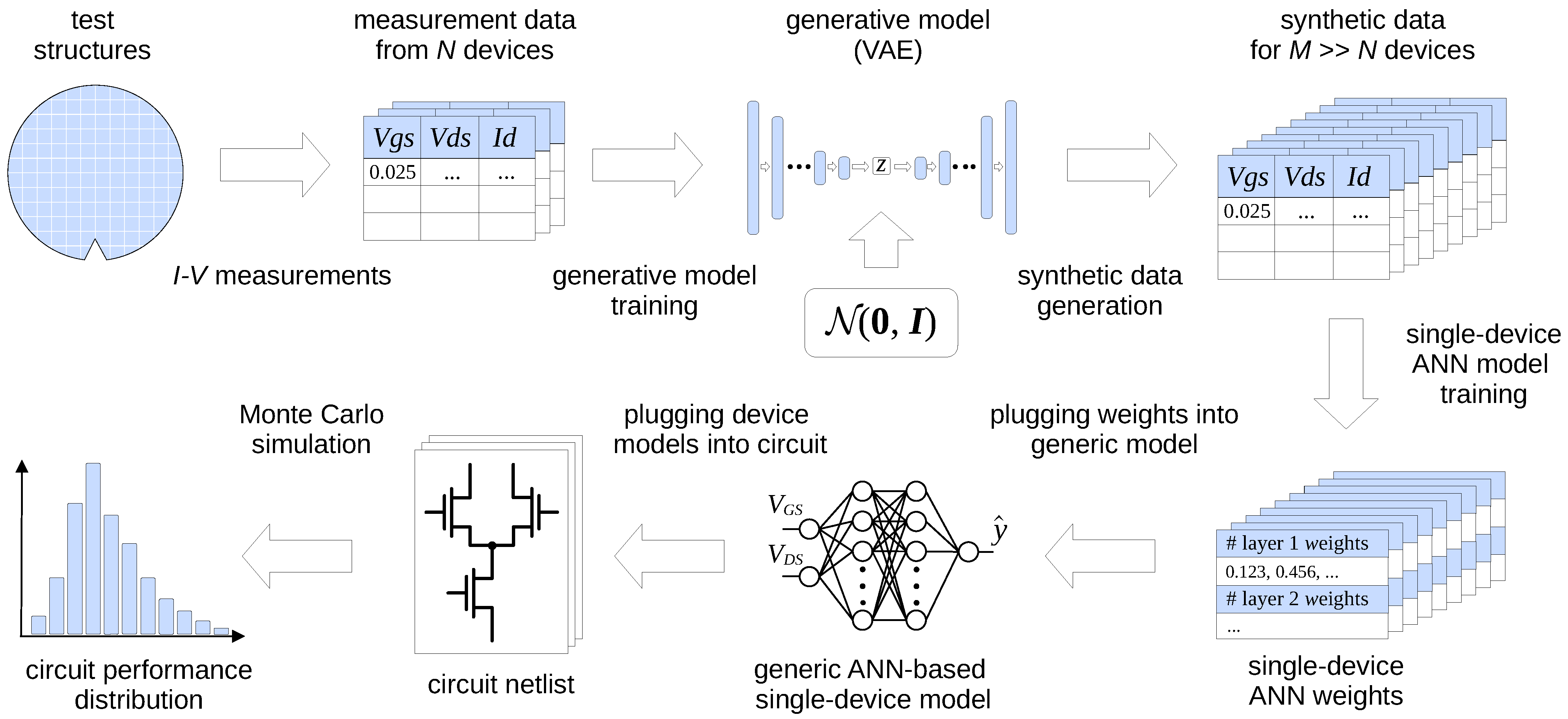
The trained model can then be used to generate data of this kind in much larger quantities (thousands or more) than the size of the training set (under a hundred). This procedure can be seen as a case of data augmentation, where a small set of real data is used to generate synthetic data points to build a dataset large enough for a given application (see, e.g., [15,16]). Since each data point is just a vector of discrete samples for a single device, an ANN-based model must be subsequently fitted to those samples to produce a continuous representation of the device’s I-V curves for Spice simulation. The entire workflow is shown in Figure 1.
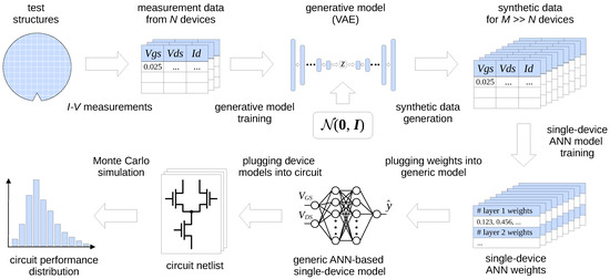
Figure 1.
Details of the proposed procedure from test structure I-V measurements through synthetic I-V data generation to statistical circuit simulation.
2. Autoencoders and Variational Autoencoders: Theoretical Background
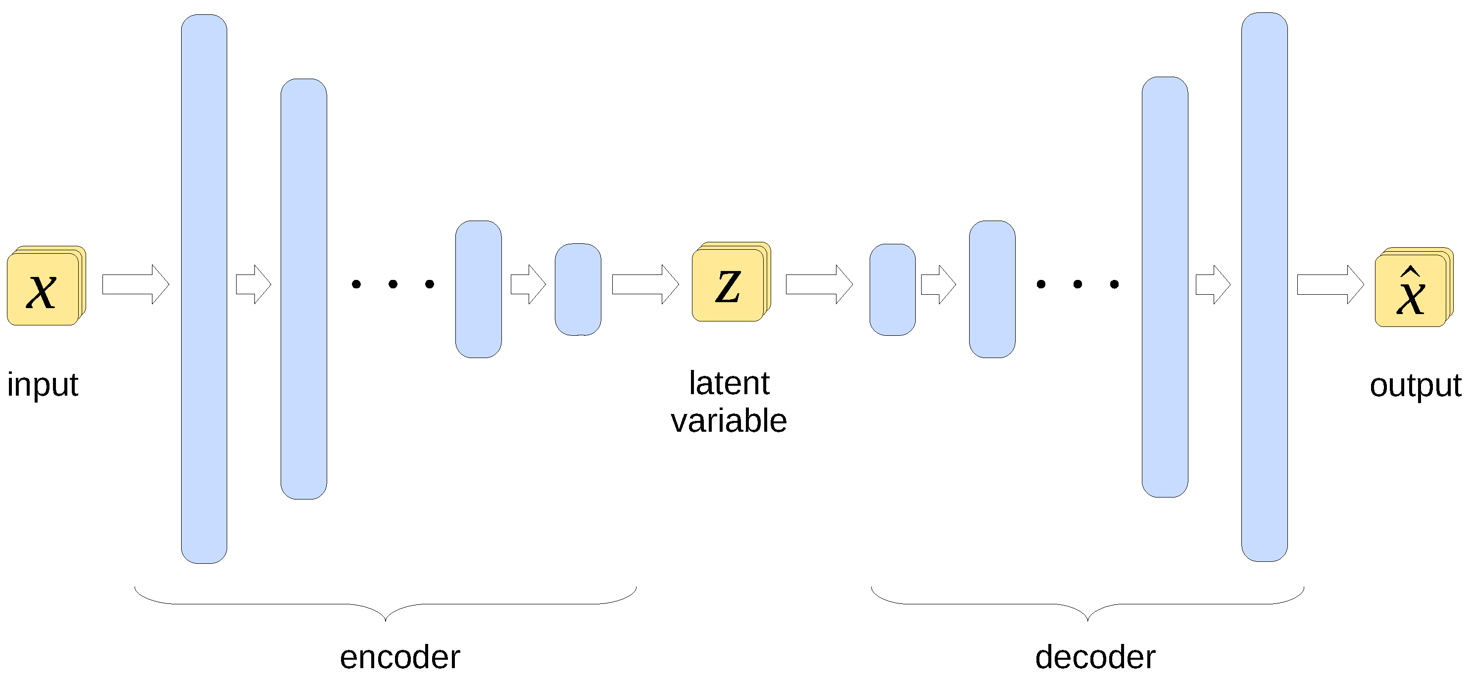
An autoencoder is a type of ANN used to find a lower-dimensional representation of its input data. The architecture of a typical autoencoder is sketched conceptually in Figure 2.
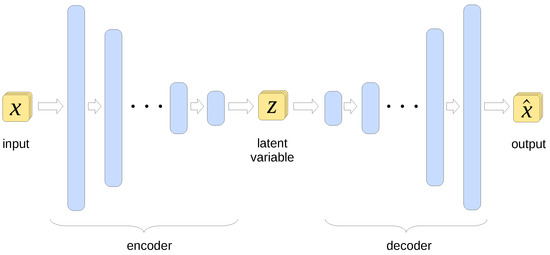
Figure 2.
Architecture of an autoencoder. The blue bars represent layers of units (artificial neurons). The bar sizes reflect the varying number of units in subsequent layers, translating into the dimension of data processed by each layer.
The high-dimensional input data vector is first propagated through subsequent layers of artificial neurons (a.k.a. units) in the part denoted as encoder, with each layer containing fewer units than its predecessor. This gradually reduces the dimensionality of the processed data, which can be seen as a form of lossy compression. The vector at the encoder output is referred to as the latent representation of the original data or just latent variable. This representation is subsequently processed by the block denoted as decoder, gradually increasing its dimensionality until it reaches the size of the original input vector. The training process involves minimizing the difference between the autoencoder’s input and its output. This forces the encoder part to produce a latent representation that preserves the essential features of the input data at the expense of less important features and noise.
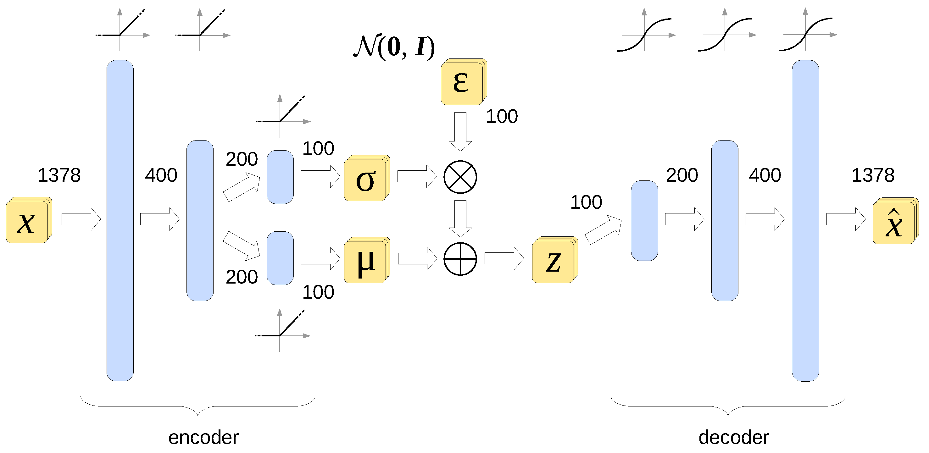
A variational autoencoder (VAE) is an extension of this concept, with the latent variable being forced during the training process to follow a known statistical distribution, usually the multidimensional standard normal distribution [17]. The architecture of the VAE used in this work is shown in Figure 3.

Figure 3.
Architecture of the variational autoencoder used in this work. Also shown are the activation functions of all layers as well as the dimensions of the data vector at each stage. All layers are fully connected.
To achieve this goal, the VAE is trained so as to minimize the following loss function:
, referred to as the reconstruction error, is the mean squared error between the encoder input and decoder output . In the context of this paper, is some function of the drain current (to be detailed in Section 3.2), and “mean” denotes an average taken over all the values of and as well as over all the observations in the minibatch. denotes the Kullback–Leibler divergence, i.e., a measure of dissimilarity between two statistical distributions, defined as
The Kullback–Leibler divergence is a non-negative quantity dropping to zero if and only if distributions P and Q are identical. In our case, is the standard normal distribution and is treated as the target. On the other hand, results from processing the input variable with the encoder. Since the encoder is a neural network with trainable parameters (weights (The term “weights” is used throughout this paper as shorthand for both weights and biases of ANN units)), may be shaped almost at will. Making a component of the loss function subject to minimization brings as close as possible to the standard normal distribution as the training progresses. The encoder is thus trained to transform the multidimensional input variable into a lower-dimensional latent standard normal variable . The decoder, on the other hand, is trained to reverse this process, i.e., to transform into an approximation of the VAE’s input . The essential feature of these transformations is that if two input vectors are close in value, they are supposed to produce similar values of . Furthermore, since the decoder is trained to reverse the transformation performed by the encoder, similar values of are transformed into similar values of . Thus, the decoder learns to perform a smooth, albeit highly nonlinear, interpolation between training examples.
Once the VAE is trained, the encoder may be discarded. The decoder is then stimulated with a random variable drawn from the multidimensional standard normal distribution. If a value of is used that has never appeared at the decoder’s input during the training phase, the decoder will produce an output that is not identical with any of its training examples and yet shares their essential statistical properties. This way, the decoder stimulated with a source or random vectors drawn from can be used as a generator of a multivariate random variable whose statistical distribution, although not given in an analytical form, is inferred from the training data. For this reason, VAEs are widely used as generative models. While their original application was generating artificial faces, they are used in other fields like text processing [18], generating audio signals [19], creating level maps for video games [20], or mapping high-dimensional search spaces into lower-dimensional ones in order to facilitate optimization [21]. However, no information regarding the use of VAEs in semiconductor device modeling has been reported in the literature.
In this work, a VAE-based model is used to generate I-V curves of a MOSFET with given nominal channel dimensions and manufactured in a process subject to perturbations. Please note that the variations in process parameters need not be known explicitly to successfully train the VAE. Also, the latent vector cannot be treated as values of any particular process parameters. In other words, no reverse engineering is performed, and the confidentiality of the process-related data is not compromised.
3. Experimental Setup
To prove the usability of the VAE as a generative model of MOSFET I-V characteristics, a series of numerical experiments was performed. “Reference” samples used to train the model were generated using Spice simulation. The number of samples obtained this way was much greater than if they came from measurements of fabricated structures. This enabled a detailed visualization of histograms of selected circuit performances for subsequent comparison with the result obtained with the proposed model. Anyway, the source of reference data (measurement vs. simulation) does not influence the workflow presented below.
3.1. Benchmark Circuit
The benchmark used to evaluate the proposed approach was a 5-stage ring oscillator (RO) built with nominally identical inverters. The performances of interest were oscillation period and power consumption. Both these figures depend on the “driving capability” of devices forming the inverters. The conventional figure of merit expressing a transistor’s driving capability is , defined as the drain-current value corresponding to both the drain and gate biased with the nominal supply voltage. As shown in Figure 4, this point is never reached, or even approached, during normal operation of a ring oscillator or clocked digital circuit. This stresses the importance of statistical characterization of a device across a wide range of biases rather than just collecting the statistics of or any other single figure of merit.
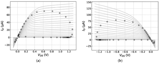
Figure 4.
The circles represent samples collected at 5 ps intervals during a single oscillation period from one n-channel and one p-channel MOSFET (Figures (a) and (b), respectively), plotted against the respective device’s output curves. The top curve corresponds to V (oscillator supply voltage); the spacing between curves is mV.
The inverters analyzed in this experiment were built with minimum-length 130 nm-node MOSFETs with a channel width of 180 nm in the n-channel devices and 680 nm in the p-channel transistors. The channel widths were chosen so as to make the inverter’s threshold voltage equal to exactly half of the supply voltage V. Three device parameters have been assumed to be subject to Gaussian variations: channel length L, threshold voltage , and source/drain resistance . The mean values and standard deviations of those parameters are summarized in Table 1. The variation is used here as a substitute for deviations in a number of process parameters like gate material work function, gate dielectric permittivity, and the profile of threshold-adjust implant as well as halo/pocket implants.

Table 1.
Mean values and standard deviations of the Gaussian distributions of the device parameters used in the ring oscillator experiment.
Two Monte Carlo experiments were conducted on such ring oscillators. In the reference simulations, the BSIM 3v3 MOSFET model was used [22]. Then, it was replaced by ANN-based generated models. The model generation details are given in the subsequent subsections. Since the current version of the generative model only produces I-V data but not yet the C-V data, the ANN-based models had to somehow use the same terminal capacitances as BSIM models for fair comparison of dynamic properties of both models. To this end, the voltage-dependent BSIM capacitances had to be replaced with such fixed values as to assure the same oscillation period. The network of fixed capacitances used in each inverter is shown in Figure 5.
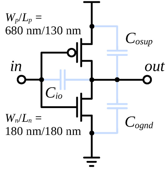
Figure 5.
Architecture of each stage of the ring oscillator. The values of the equivalent capacitances are fitted separately for each supply voltage value.
represents the sum of gate-to-channel and gate-to-drain overlap capacitances of both devices. represents the drain-to-substrate capacitance of the n-channel device shown in the figure plus the gate-to-source overlap capacitance of the n-channel device in the next stage. plays a similar role in the p-channel devices. The values of those three equivalent capacitances have been tuned so as to produce a waveform identical with the one obtained with the BSIM capacitances enabled. Since MOSFET capacitances are highly voltage dependent, this procedure had to be repeated separately every time the supply voltage had been changed. The extracted equivalent capacitances were subsequently used both in the reference Monte Carlo simulations (using BSIM models) and, later, in the simulations with the proposed ANN-based models.
3.2. VAE-Based Generative Model of MOSFET I-V Data
The architecture of the model used to generate MOSFET I-V data is presented in Figure 3. The model has been implemented in Python using the Pytorch library [23]. A single data point in the training set was the family of samples from a single device. was swept from 0 V to V with a fixed step of 25 mV, while was swept from 50 mV to V with a 50 mV step. The procedure for p-channel devices was identical, but all the voltages were negative. Thus, each device was described with numbers.
Using as the VAE input works fine for above the threshold voltage . However, values below the threshold are many orders of magnitude smaller, so they have hardly any contribution to the training loss function. As a consequence, the VAE does not even attempt to minimize the reconstruction error in subthreshold. A common solution is to make the ANN reproduce the logarithm of rather than itself. Such a transformation, however, brings the above- and below-threshold values to the same order of magnitude and, as a consequence, almost equalizes the relative error across the whole range. This is not desirable because relative-error levels that are acceptable for the off-current are too high for the on-current. Therefore, in this work, the subthreshold regime has been slightly deprioritized by defining each component of the VAE input vector in the following way:
where the normalizing current fA. This value was chosen because it is an order of magnitude below the smallest current observed in the dataset. Therefore, this choice of guarantees that the argument of the logarithm in (3) is always greater than unity, which leads to positive logarithm values.
Various variants of the VAE architecture have been tested, namely,
- Number of layers in both decoder and encoder ranging from three to five.
- The number of units in the encoder’s input layer and decoder’s output layer varying between 100 and 800, with all the other layers modified accordingly.
- The following combinations of activation functions in the decoder and encoder:
- –
- ReLU (Rectified Linear Unit) in all layers,
- –
- sigmoid in all layers,
- –
- sigmoid in the last layer, ReLU in the rest,
- –
- ReLU in the last layer, sigmoid in the rest.
- Convolutional layers instead of fully connected ones.
The parameters of the final VAE can be found in Figure 3. All the layers are fully connected. While convolutional layers are commonly used in VAEs whose goal is generation of images, this approach turned out to produce extremely noisy results in our case. The probable reason is the small size of the training sets used in this experiment. Please note that the key point of the proposed generative model is its ability to be trained on data from devices that cannot be easily characterized in large quantities either due to their experimental character or because of the extreme conditions in which they operate. As a result, the training datasets used in this work are several orders of magnitude smaller than those used to train convolutional neural networks presented in the literature (for example, in applications described in Section 2.2 of [20], training sets of cases have been used).
The final encoder architecture consists of three layers, whose output vectors have a length of 400, 200, and 100, respectively, with the last number being the size of the latent variable z. All the units in the encoder have the ReLU activation function. The layers in the decoder expand the latent variable to 200, 400, and finally 1378 dimensions. All the units in the decoder have the sigmoid activation function. The batch size used in training was 25, except for the smallest training set consisting of 20 examples, where the batch size had to be reduced to 5. Increasing the batch size over 25 items led to greater reconstruction errors.
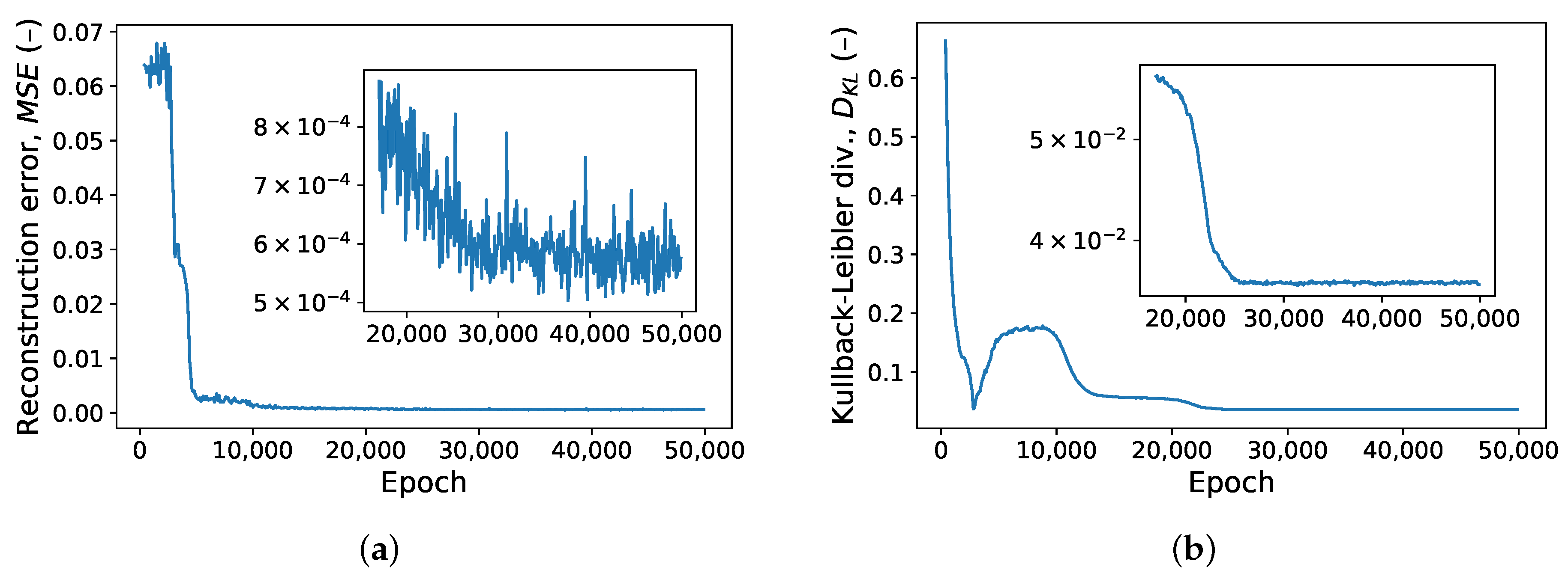
A validation set of 1000 devices was used all through the training process to monitor both components of the loss, i.e., the reconstruction error and Kullback–Leibler divergence. Typical learning curves for those two error components are shown in Figure 6. The training was interrupted after both error components saturated. This happened after 5000 to epochs, with smaller training sets requiring more epochs. (An epoch marks the point in an ANN training process where each training example has been used exactly once. Multiple epochs are usually required, with the dataset randomly shuffled between them). The entire process took about five minutes on a desktop computer with computations offloaded to an NVIDIA GeForce GTX 1660 SUPER GPU.

Figure 6.
(a) VAE reconstruction error and (b) Kullback–Leibler divergence (KLD) on the validation dataset evaluated in the training phase every 100 epochs. The insets show that the KLD saturates after approximately epochs, while the reconstruction error takes approximately twice as long to reach its minimum.
The optimal contribution of Kullback–Leibler divergence in the loss function (see Equation (1)) was experimentally found to be . Larger values of excessively prioritized the normality of the latent variable over reconstruction accuracy. The I-V curves reconstructed by the decoder in this case either showed excessive ripples or, while preserving satisfactory smoothness, deviated heavily from the input data. On the other hand, reducing below did not visibly improve the quality of reconstructed I-V curves while making the latent-variable distribution significantly deviate from , thus precluding later use of the decoder as a source of I-V curves sharing the statistical properties with the training data.
After training, the VAE was once again used to encode a subset of the validation dataset. The Henze–Zirkler test for multivariate normality was subsequently performed on the latent variable to make sure its distribution was sufficiently close to normal [24]. The test passed over of the time, which shows that the latent variable is indeed close to normal.
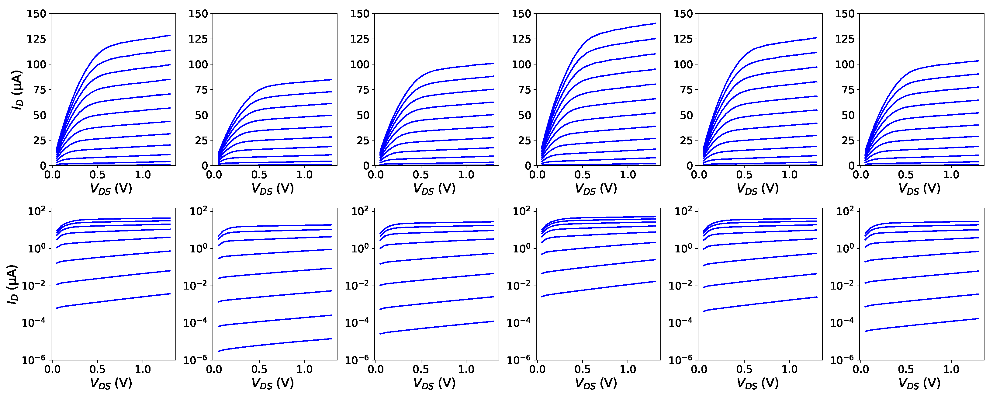
Figure 7 shows example I-V curves generated by a VAE trained on a dataset of 50 devices and subsequently stimulated with six standard normal vectors. The curves are qualitatively similar to actual MOSFET curves (presented in Figure 4a) both on the linear scale (top row) and logarithmic scale (bottom row). Ripples are very small and are further smoothed out at the next stage, where ANN-based approximation models are fitted individually to the I-V curves of each device (see the following Section).
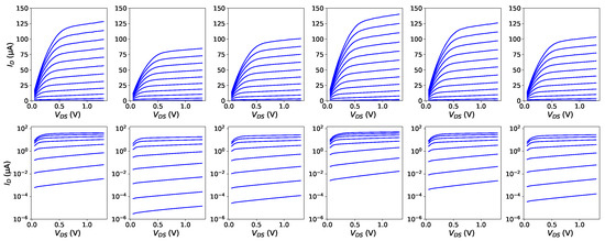
Figure 7.
Example sets of I-V curves generated by the presented VAE plotted on the linear (top row) and logarithmic scale (bottom row). The curves correspond to bias ranges (top) and (bottom) with a step of 100 mV.
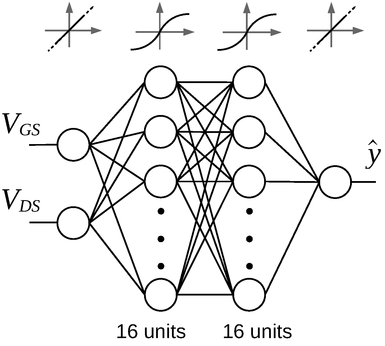
3.3. ANN-Based Models of Single Devices
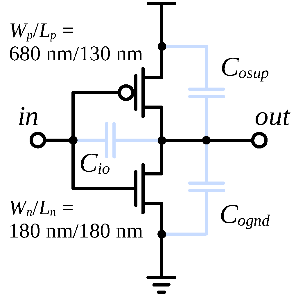
The VAE presented in the previous Section generates a device’s I-V response as a set of discrete points. To make this model usable, some interpolation between them is necessary. The approach taken in this work uses ANNs fitted individually to every device. These ANNs, whose architecture is presented in Figure 8, were composed of the following layers:

Figure 8.
Architecture of the fully-connected ANN used to model individual devices. Also shown are the activation functions of all the layers and the sizes of hidden layers.
- Input layer: 2 linear units receiving and as their inputs.
- First hidden layer: 16 sigmoid units.
- Second hidden layer: 16 sigmoid units.
- Output layer: 1 linear unit producing response (see below).
For reasons outlined in Section 3.2, the ANN output was a function of the logarithm of the device drain current . This, however, posed a problem at , which takes place at . Therefore, this particular bias was not used in the training set. To make the model correctly reproduce a MOSFET’s behavior at zero drain-to-source bias anyway, it is common to train the ANN using the following expression (see, e.g., [7,10,11]):
At the inference stage, when the model is used in the simulator to produce a response , this expression is solved for :
which forces at . This approach has been adopted in this work. However, like in the VAE presented in Section 3.2, it resulted in excessive prioritization of the subthreshold region, leading to unacceptably high error levels above the threshold. This effect was reversed by using the following sigmoid weighting function:
where V for n-channel devices and V for p-channel devices. Finally, (4) and (6) were combined to form the loss function used at the training stage:
The ANN training was performed in Pytorch. The training of ANN models of individual devices can be greatly sped up by exploiting the relative similarity of the I-V responses of all the devices of the same channel type and size, which implies similar values of the weights of their models. This allows reusing the weights of the first successfully trained model as an initial guess in training the models of all the subsequent devices of the same type. While training the ANN model from scratch lasts on average 31 s per device on a desktop computer, this time is reduced to s when reusing a previously generated model as the initial guess. Thus, this simple technique provides a speedup of almost times.
The model of individual devices (referred to as the single-device model) is split in two parts. A generic Verilog-AMS file is common to all devices, while weights, distinct to individual devices, are stored in separate files included in the main file during simulation. These two parts can then be loaded into a circuit simulator like Synopsys HSPICE® (used in this experiment) or Cadence Spectre®. For every device instance and every Monte Carlo run, a new set of weights is read into the generic model.
4. Results
The setup presented in the previous section was used in a series of Monte Carlo experiments to assess the feasibility of the proposed approach. Of particular interest was the influence of the training set size on the accuracy of reproducing the statistical distribution of the RO period and power consumption. Training sets of 20, 50, 150, and 500 instances were tried for each device type. In a real-world setting, the proposed generative model will have to be trained based on measurement data coming from a relatively small set of test structures. This is in contrast to more “conventional” tasks like image generation, where a model is trained on datasets containing thousands or tens of thousands of images. By way of example, the training dataset of the MNIST database of images of handwritten digits frequently used as a benchmark for many machine learning algorithms, including generative models, contains 6000 images of each digit.
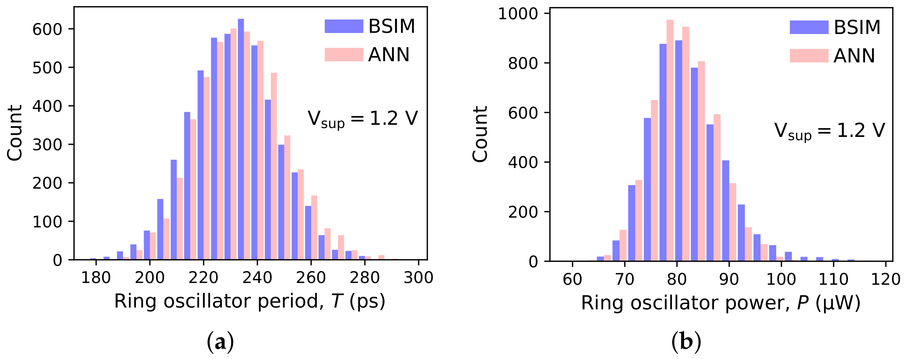
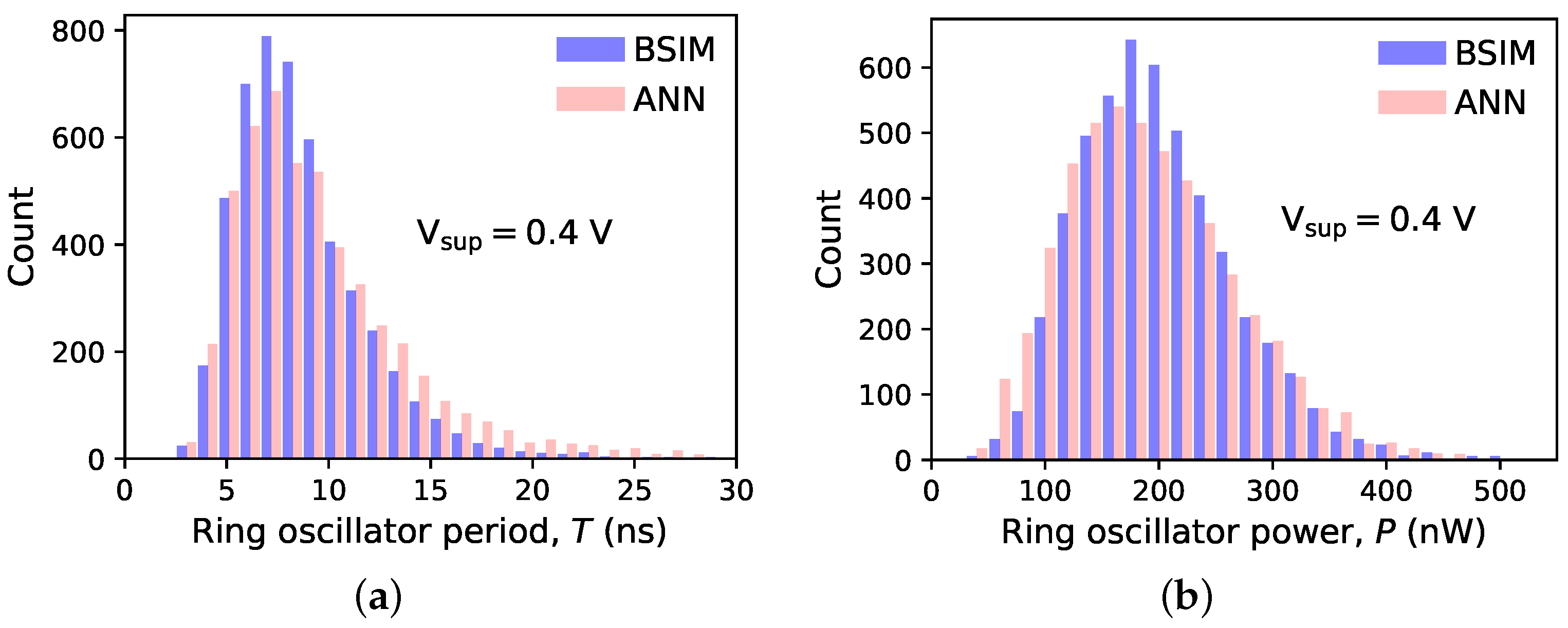
Two experiments were run, differing in the ring oscillator supply voltage. In the first experiment, the nominal supply voltage for the 130 nm MOSFET node V was used. In the other, was reduced to V, which corresponds to devices operating slightly above the threshold voltage or, for strong positive deviations in , in subthreshold (see Table 1 for mean values and standard deviations of ). A total of 5000 ROs were generated in either experiment, each with unique ANN-based models of n-channel and p-channel devices. By way of reference, another 5000 ROs were simulated with BSIM models. Histograms of the RO period and power consumption are presented in Figure 9 ( V) and Figure 10 ( V).

Figure 9.
Histograms of (a) period and (b) power consumption of 5000 ring oscillators described in Section 3.1. The ANN-based device models were generated by VAEs trained using 50 instances per device type. BSIM results serve as a reference.
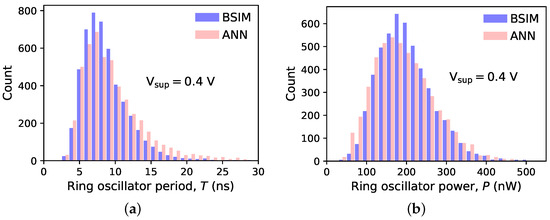
Figure 10.
Histograms of the (a) period and (b) power consumption of 5000 ring oscillators with devices operating in moderate inversion ( V). The ANN-based device models were generated by VAEs trained using 50 instances per device type. BSIM results serve as a reference.
As shown in Figure 9 and Figure 10, the statistical distributions of the oscillation period and power consumption display a significant skewness. This is especially true at lower supply voltages, i.e., with devices working in weak and moderate inversion, where the relationship between the drain current and the parameters subject to variations (mostly channel length and threshold voltage) is close to exponential. Such distributions cannot be accurately described with just the mean value and standard deviation. More information is conveyed by percentiles. The X-th percentile, here denoted as , is defined as the value that is not exceeded by the random variable more often than X-percent of the time. Thus, is the median, while is the value exceeded only by the top cases. Selected percentiles of the RO period and power for both values of are given in Table 2.
Table 2.
Selected percentiles of the ring oscillator period and power consumption based on 5000 Monte Carlo Spice runs. BSIM results (bottom row) serve as a reference. Other results were obtained with the proposed procedure using a generative model trained on datasets of varying sizes.
5. Discussion
The histograms of the ring oscillator period and power consumption obtained with the proposed model are in good agreement with BSIM-based simulations. Thus, the generative model reproduces well the statistical properties of the I-V curves of devices used for its training. The agreement is satisfactory even for near-threshold operation ( V), where the relationship between the perturbed device parameters and the drain current is close to exponential, i.e., strongly nonlinear. As a result, the values of period and power span an entire order of magnitude, and their distributions show a pronounced skewness. The numerical data presented in Table 2 show that even the top percentiles and , corresponding to the long right tails, can be predicted with a reasonable accuracy. This is important because the right tails of the power and period distributions directly influence the parametric yield of a digital circuit. For training sets of 150 devices, all percentiles are estimated within 5 percent of their true value (and in most cases within 2 percent). For training sets of 20 and 50 devices, the errors are closer to 10 percent and, for , sometimes larger. It must be remembered, however, that is defined as the value that is exceeded only by 1 percent of the population. Estimating this quantity with a model trained on just 20 or 50 observations is necessarily prone to error. Still, the number of training cases used in this experiment is several orders of magnitude smaller than what is normally used in image-generation applications. Unlike images of faces, digits, or other objects, MOSFET drain current plotted in the space forms a relatively smooth surface. Also, differences between individual cases are quite subtle. Thus, a relatively small set of training examples may capture all the necessary statistical properties of the entire population. Interestingly, there is no clear relationship between the accuracy of period and power estimation and training set size. An increase in error seems to occur when both go below 50 cases and above 150 cases.
Please note that the I-V curves were sampled on a fixed uniform grid. Lowering the RO operating voltage from V to V means that samples corresponding to two-thirds of biases and the same proportion of biases were left unused. Still, even in such conditions, the histograms obtained with the proposed model look very close to those coming from the BSIM simulations.
A single RO simulation took an average of 161 ms with the BSIM model and 886 ms with the ANN-based model. Thus, the currently used Verilog-AMS-based implementation of the proposed model is approximately times slower than BSIM. One may expect that implementing the model directly in the simulator source code would significantly speed up the simulation.
To sum up, the proposed method seems attractive because I-V characterization of 20–50 transistors is often feasible even in cases of emerging devices or ones working in a cryogenic cooler.
Currently, the proposed model only generates I-V data. It can be extended to also include MOSFET transcapacitances, defined as:
where i and j denote device terminals. This, however, would mean a significant increase in the size of the VAE input layer and, as a consequence, other layers. In the simplest case of a three-terminal device like the FinFET or the gate-all-around MOSFET, one must consider six transcapacitances: , , , , , and (the source terminal serves as a reference, so its potential is fixed). For a bulk MOSFET, where the substrate must be considered as another terminal, the number of transcapacitances grows to 12. Please note that one cannot dedicate separate VAEs to each of those capacitances because correlation between their statistical distributions would be lost. Therefore, a single VAE is needed. Its input vector, in addition to the data used in the presented work, will also contain , , etc. The generative model in its current form takes single minutes to train. Including transcapacitances in the training set, and thus expanding the ANN layer sizes by an order of magnitude, would likely increase the training time to many hours, which still is not a prohibitive task.
Author Contributions
Conceptualization, D.K.; methodology, D.K.; software, D.K.; validation, D.K.; formal analysis, D.K.; investigation, D.K.; resources, D.K.; data curation, D.K.; writing—original draft preparation, D.K.; writing—review and editing, D.K.; visualization, D.K.; supervision, D.K.; project administration, G.K.; funding acquisition, G.K. All authors have read and agreed to the published version of the manuscript.
Funding
This research was funded by the National Centre for Research and Development of Poland, grant QUANTERAII/1/80/SIQCI/2022.
Institutional Review Board Statement
Not applicable.
Data Availability Statement
Datasets available on request.
Conflicts of Interest
The authors declare no conflicts of interest. The funders had no role in the design of the study; in the collection, analyses, or interpretation of the data; in the writing of the manuscript; or in the decision to publish the results.
Abbreviations
The following abbreviations are used in this manuscript:
| ANN | Artificial neural network |
| KLD | Kullback–Leibler divergence |
| MOSFET | Metal-oxide-semiconductor field-effect transistor |
| MSE | Mean squared error |
| PDK | Process design kit |
| RO | Ring oscillator |
| VAE | Variational autoencoder |
References
- Beckers, A.; Jazaeri, F.; Enz, C. Cryogenic MOS Transistor Model. IEEE Trans. Electron Devices 2018, 65, 3617–3625. [Google Scholar] [CrossRef]
- Kimura, M.; Inoue, S.; Shimoda, T. Table Look-Up Model of Thin-Film Transistors for Circuit Dimulation Using Spline Interpolation with Transformation by y = x + log(x). IEEE Trans. Comput.-Aided Des. Integr. Circuits Syst. 2002, 21, 1101–1104. [Google Scholar] [CrossRef]
- Yang, B.; McGaughy, B. An Essentially Non-Oscillatory (ENO) High-Order Accurate Adaptive Table Model for Device Modeling. In Proceedings of the 41st Design Automation Conference, San Diego, CA, USA, 7–11 June 2004; pp. 864–867. [Google Scholar]
- Bourenkov, V.; McCarthy, K.; Mathewson, A. MOS table models for circuit simulation. IEEE Trans. Comput.-Aided Des. Integr. Circuits Syst. 2005, 24, 352–362. [Google Scholar] [CrossRef]
- Thakker, R.A.; Sathe, C.; Sachid, A.B.; Shojaei Baghini, M.; Ramgopal Rao, V.; Patil, M.B. A Novel Table-Based Approach for Design of FinFET Circuits. IEEE Trans. Comput.-Aided Des. Integr. Circuits Syst. 2009, 28, 1061–1070. [Google Scholar] [CrossRef]
- Xu, J.; Gunyan, D.; Iwamoto, M.; Horn, J.M.; Cognata, A.; Root, D.E. Drain-Source Symmetric Artificial Neural Network-Based FET Model with Robust Extrapolation Beyond Training Data. In Proceedings of the 2007 IEEE/MTT-S International Microwave Symposium, Honolulu, HI, USA, 3–8 June 2007; pp. 2011–2014. [Google Scholar] [CrossRef]
- Wang, J.; Kim, Y.H.; Ryu, J.; Jeong, C.; Choi, W.; Kim, D. Artificial Neural Network-Based Compact Modeling Methodology for Advanced Transistors. IEEE Trans. Electron Devices 2021, 68, 1318–1325. [Google Scholar] [CrossRef]
- Wang, J.; Xu, N.; Choi, W.; Lee, K.H.; Park, Y. A Generic Approach for Capturing Process Variations in Lookup-Table-Based FET Models. In Proceedings of the 2015 International Conference on Simulation of Semiconductor Processes and Devices (SISPAD), Washington, DC, USA, 9–11 September 2015; pp. 309–312. [Google Scholar] [CrossRef]
- Kasprowicz, D. Table-Based Model of a Dual-Gate Transistor for Statistical Circuit Simulation. IEEE Trans. Comput.-Aided Des. Integr. Circuits Syst. 2019, 38, 1493–1500. [Google Scholar] [CrossRef]
- Woo, S.; Jeong, H.; Choi, J.; Cho, H.; Kong, J.T.; Kim, S. Machine-Learning-Based Compact Modeling for Sub-3-nm-Node Emerging Transistors. Electronics 2022, 11, 2761. [Google Scholar] [CrossRef]
- Lyu, Y.; Chen, W.; Zheng, M.; Yin, B.; Li, J.; Cai, L. Machine Learning-Assisted Device Modeling With Process Variations for Advanced Technology. IEEE J. Electron Devices Soc. 2023, 11, 303–310. [Google Scholar] [CrossRef]
- Mehta, K.; Raju, S.S.; Xiao, M.; Wang, B.; Zhang, Y.; Wong, H.Y. Improvement of TCAD Augmented Machine Learning Using Autoencoder for Semiconductor Variation Identification and Inverse Design. IEEE Access 2020, 8, 143519–143529. [Google Scholar] [CrossRef]
- Mehta, K.; Wong, H.Y. Prediction of FinFET Current-Voltage and Capacitance-Voltage Curves Using Machine Learning With Autoencoder. IEEE Electron Device Lett. 2021, 42, 136–139. [Google Scholar] [CrossRef]
- Foster, D.; Friston, K. Generative Deep Learning: Teaching Machines to Paint, Write, Compose, and Play; O’Reilly Media, Incorporated: Sebastopol, CA, USA, 2023. [Google Scholar]
- Shorten, C.; Khoshgoftaar, T.M. A Survey on Image Data Augmentation for Deep Learning. J. Big Data 2019, 6, 60. [Google Scholar] [CrossRef]
- Gao, J.; Heng, F.; Yuan, Y.; Liu, Y. A novel machine learning method for multiaxial fatigue life prediction: Improved adaptive neuro-fuzzy inference system. Int. J. Fatigue 2024, 178, 108007. [Google Scholar] [CrossRef]
- Kingma, D.P.; Welling, M. Auto-Encoding Variational Bayes. In Proceedings of the 2nd International Conference on Learning Representations, ICLR 2014, Banff, AB, Canada, 14–16 April 2014; Conference Track Proceedings. 2014. Available online: http://arxiv.org/abs/1312.6114v10 (accessed on 6 March 2023).
- Miao, Y.; Yu, L.; Blunsom, P. Neural Variational Inference for Text Processing. In Proceedings of the ICML, New York, NY, USA, 19–24 July 2016; Volume 48, pp. 1727–1736. [Google Scholar]
- Karamatlı, E.; Cemgil, A.T.; Kırbız, S. Audio Source Separation Using Variational Autoencoders and Weak Class Supervision. IEEE Signal Process. Lett. 2019, 26, 1349–1353. [Google Scholar] [CrossRef]
- Mak, H.W.L.; Han, R.; Yin, H.H.F. Application of Variational AutoEncoder (VAE) Model and Image Processing Approaches in Game Design. Sensors 2023, 23, 3457. [Google Scholar] [CrossRef] [PubMed]
- Touloupas, K.; Sotiriadis, P.P. Mixed-Variable Bayesian Optimization for Analog Circuit Sizing through Device Representation Learning. Electronics 2022, 11, 3127. [Google Scholar] [CrossRef]
- Cheng, Y.; Hu, C. MOSFET Modeling and BSIM3 User’s Guide; Kluwer Academic Publishers: Norwell, MA, USA, 1999. [Google Scholar]
- Pytorch Library for Deep Learning in Python. Available online: https://pytorch.org (accessed on 6 March 2023).
- Henze, N.; Zirkler, B. A Class of Invariant Consistent Tests for Multivariate Normality. Commun. Stat.-Theory Methods 1990, 19, 3595–3617. [Google Scholar] [CrossRef]

Disclaimer/Publisher’s Note: The statements, opinions and data contained in all publications are solely those of the individual author(s) and contributor(s) and not of MDPI and/or the editor(s). MDPI and/or the editor(s) disclaim responsibility for any injury to people or property resulting from any ideas, methods, instructions or products referred to in the content. |
© 2024 by the authors. Licensee MDPI, Basel, Switzerland. This article is an open access article distributed under the terms and conditions of the Creative Commons Attribution (CC BY) license (https://creativecommons.org/licenses/by/4.0/).