Article

Design of a Sigma-Delta Analog-to-Digital Converter Cascade Decimation Filter

1
School of Microelectronics, Tianjin University, Tianjin 300072, China
2
Tianjin Key Laboratory of Imaging and Sensing Microelectronics, Tianjin 300072, China
*
Author to whom correspondence should be addressed.
Electronics 2024, 13(11), 2090; https://doi.org/10.3390/electronics13112090
Submission received: 1 April 2024 / Revised: 20 May 2024 / Accepted: 21 May 2024 / Published: 27 May 2024

Abstract

:
As the current mainstream high-precision ADC architecture, sigma-delta ADC is extensively employed in a wide range of domains and applications. This paper presents the design of a highly efficient cascaded digital decimation filter for sigma-delta ADCs, emphasizing the suppression of high folding band noise and the achievement of a flat passband. Additionally, this study addresses the critical balance between filter performance and power consumption. An inserting zero (IZ) filter is incorporated into a cascaded integrator comb (CIC) filter to enhance aliasing suppression. The IZ filter and compensation filter are optimized using the particle swarm optimization (PSO) algorithm to achieve greater noise attenuation and smaller passband ripple. The designed filter achieves a noise attenuation of 93.4 dB in the folding band and exhibits an overall passband ripple of 0.0477 dB within a bandwidth of 20 KHz. To decrease the power consumption in the filter design, polyphase decomposition has been applied. The filter structure is implemented on an FPGA, processing a 5-bit stream from a 64-times oversampling rate and third-order sigma-delta modulator. The signal-to-noise ratio (SNR) of the output signal reaches 91.7 dB. For ASIC design, the filter utilizes 180 nm CMOS technology with a power consumption of 0.217 mW and occupies a layout area of 0.72 mm2. The post-layout simulation result indicates that the SNR remains at 91.7 dB.

1. Introduction

As semiconductor technology continues to advance rapidly, the demand for high-precision signal acquisition and processing is on the rise. Sigma-delta ADCs are widely used in aerospace, biomedical, and other fields due to their high-resolution characteristics. The complete sigma-delta ADC is composed of two parts, including the modulator and the decimation filter. The modulator uses noise shaping and oversampling techniques to improve the SNR [1,2], while the latter filters out the out-of-band noise and downsamples the oversampling rate data to Nyquist frequency. To achieve a high decimation rate, a single-stage decimation filter often requires thousands of orders, which consumes huge resources, and it is difficult to meet the requirements of high stopband suppression and flat passband. Therefore, the common sigma-delta ADC digital decimation filter is usually a cascade structure of a CIC filter, compensation filter, and FIR filter [3,4,5].
In the cascaded filter structure, a cascaded integrator comb (CIC) filter is often employed as the initial stage for achieving high-rate decimation. However, CIC filters are prone to the issue of passband attenuation, necessitating the integration of a compensation filter design to mitigate this limitation [4]. In addition, the reduced sampling rate may introduce aliasing noise in the folding band of the CIC [6], which will degrade the signal quality after decimation. To improve the aliasing suppression of folding bands, researchers often focus on sharpened CIC filters (SCIC filters) [7,8,9] and IZ filters [10,11]. The SCIC usually adopts the method of adding more filter orders, which consumes more resources and requires higher design requirements for the post-stage compensation filter. The authors of [7] presented methods based on minimax error criterion to design an SCIC filter. In [8], compensators with a low number of coefficients are proposed based on maximally flat error criterion. The method in [9] uses linear programming optimization technology to obtain a SCIC filter with no need of compensate filters. The IZ filter widens the folding band by adding zeros in order to obtain better noise suppression ability. The authors of [10] proposed a modified CIC filter in which zeros are sufficiently separated to increase the width of the folding bands. In [11], aliasing suppression is improved by separating and inserting zeros. To achieve a more flexible design, the IZ filter is used to improve aliasing suppression ability.
Apart from the aliasing problem in folding bands, CIC filters also suffer from significant passband attenuation, necessitating the introduction of compensating filter design [12,13,14]. The magnitude response of the compensation filter is an upward trend to compensate the CIC filter with a downward trend. The authors of [12] presented a compensate filter that is a cascade of two sinusoidal form multiplier-less filters. In [13], the PSO algorithm is applied in the improvement of integer programming for designing CIC compensators. For an SCIC filter designed using the minimax technique, a compensation filter with a multiphase decomposition structure is designed in [14].
To meet the high-performance requirements of sigma-delta ADC decimation filters, a cascade structure of decimation filters with strong aliasing suppression and low passband ripple is designed. The cascade filter consists of a CIC filter, a compensation filter, and a half-band filter. To address the issue of insufficient aliasing suppression in the folding band of the CIC filter, zero interpolation is employed to enhance the anti-aliasing capability of the CIC filter. The novelty of this work lies in the application of the PSO algorithm to optimize the coefficient configuration of the filter; aliasing suppression is further strengthened, and better passband flatness is achieved. In addition, low power consumption is obtained by applying polyphase decomposition in filter design.

2. Digital Decimation Filter Architecture

The front-end circuit of the decimation filter designed in this paper is a third-order, single-loop, 5-bit, quantized sigma-delta modulator. Operating with a clock frequency of 2.56 MHz, this modulator samples and quantizes analog signals with an oversampling ratio of 64. The decimation filter consists of three stages; the first stage is a CIC filter, the second stage is a CIC compensation filter, and the last stage is a half-band filter. Specifically, the 2.56 MHz 5-bit quantized data stream generated by the modulator initially passes through the CIC filter, where it undergoes a 32-times downsampling to 80 KHz. Next, these downsampled data are processed by the compensation filter, which does not perform further downsampling but instead compensates for the passband attenuation introduced by the CIC filter. Finally, the half-band filter executes a two-times downsampling on the 80 KHz stream originating from the compensation filter, effectively restoring it to the Nyquist frequency. The complete process described above is shown in Figure 1.

2.1. CIC Decimation Filter

CIC filters are characterized by a simple structure with all filter coefficients set to one. This attribute eliminates the need for multipliers in the hardware implementation, rendering them highly suitable for high-rate decimation filtering as the initial stage in a cascaded filter structure. The transfer function of a traditional CIC filter is as follows:
H ( z ) = 1 M 1 z M 1 z 1 K
In Formula (1), M is the decimation factor of the CIC filter, and K is the order of the CIC filter, which is usually determined by the order of the front-end modulator. Assuming that the modulator order is L, K is usually L + 1 in order to maintain a high noise suppression level [15].
The traditional CIC filter transfer function can be rewritten as follows:
H K ( z ) = 1 M j = 0 M 1 z j K = 1 M F ( z ) K
Taking the second-order CIC filter as an example, F(z) has the following:
F 2 ( z ) = 1 + 2 z 1 + + M z ( M 1 ) + + 2 z [ 2 ( M 1 ) 1 ] + z 2 ( M 1 )
By solving F2(z), we can see that the polynomial has M − 1 pairs of overlapped zeros. It can be known from [10] that broadening the CIC amplitude–frequency response curve in the folding band can effectively improve the ability to suppress aliasing noise. In this paper, we use a method that first disperses the zeros of the CIC filter and then inserts zeros into the folding band to achieve this goal.
In order to disperse the zeros of the traditional CIC filter, the middle term coefficient M in Formula (3) can be adjusted, denoted as follows:
F 2 ( z ) = 1 + 2 z 1 + + M z ( M 1 ) + + 2 z [ 2 ( M 1 ) 1 ] + z 2 ( M 1 )
where M′ is the adjusted value of the coefficient M. According to the theory of [16], in order to ensure that the roots of the polynomial after solving are all on the unit circle (that is, to ensure the stability of the system), each root of the polynomial needs to be real, and its value must be on the interval [–2, 2]. In order to reduce the resource overhead and facilitate the hardware implementation of the filter coefficient, this paper selects the second-order CIC filter for zero dispersion, and M’ is selected as (M − 0.5), then the filter transfer function is as follows:
I 1 ( z ) = 1 M 1 z M 1 z 1 2 2 1 z ( M 1 )
In order to insert zeros into the folding band, the zero points on the unit circle need to be deflected to a certain extent. For single-order CIC filters, there are the following:
H b ( z ) = 1 M j = 0 M 1 z j = 1 M j = 0 M 1 z j z M 1 = 1 M G ( z ) z M 1
Therefore, finding the root of the CIC filter is to solve for G(z). To deflect the zero of G(z), consider the polynomial GIZ(z) as follows:
G I Z ( z ) = 1 + α ( z + z 2 + + z M 2 ) + z M 1
According to study [17], in order to make the root of GIZ(z) solution on the unit circle, α must satisfy the following range:
2 M 2 α 2
In order to further broaden the amplitude–frequency response curve of the folding band, we choose to take the zeros of the traditional CIC filter as a center and insert zeros in both the left and right parts within the scope of the folding band. It can be obtained that the transfer function of this part of the filter is as follows:
I 2 ( z ) = 1 + B 1 i = 1 M 2 2 z i + z ( M 2 1 ) × 1 + B 2 i = 1 M 2 2 z i + z ( M 2 1 )
The IZ filter transfer function is as follows:
I ( z ) = I 1 ( z ) × I 2 ( z )
In addition, the hierarchical implementation and order reduction of traditional CIC filters are implemented to reduce computational complexity and save hardware resources. The transfer functions of the two-stage CIC filter are as follows:
H 1 ( z ) = 1 M 1 1 z M 1 1 z 1 K 1
H 2 ( z ) = 1 M 2 1 z M 2 1 z 1 K 2
where M1, K1, M2, and K2 are the decimation factors and orders of the two-stage CIC filters, respectively. The first stage of the proposed CIC filter is used for higher multiple decimation. The second stage works at a lower frequency and makes a greater contribution to the first folding band of CIC. Therefore, the IZ filter and the second-stage CIC are mix-designed, and M in Formulas (5) and (9) takes the value of M2. The CIC filter transfer function after zero interpolation is as follows:
H I ( z ) = H 1 ( z ) H 2 ( z M 1 ) I ( z M 1 )
The selection of four design parameters (M1, K1, M2, K2) for the two-stage CIC filter is generally a balance among resource consumption, folding band aliasing suppression ability, and power consumption. The following principles should be observed:
(1)
The decimation factor of the former stage should be higher than that of the latter stage to reduce the resource and power consumption of the IZ filter, which has a more complex structure.
(2)
Increasing the CIC order can improve the anti-aliasing characteristics of the CIC filter.
(3)
According to Formula (9), the obtained decimation multiple of the latter stage CIC should be more than three.
The filter design parameters selected in this paper are M1 = 8, K1 = 4, M2 = 4, and K2 = 3. Taking B1 = 3/2, B2 = 1/2 in (9) as an example, a pole-zero plot is shown in Figure 2. It can be seen that by adding the IZ filter, the zeros of the traditional CIC filter have been separated and new zeros have been added. The amplitude–frequency characteristic is shown in Figure 3 (the pink dashed lines indicates the range of the folding band, same in Figure 6); the folding band of the CIC filter is effectively expanded, and the attenuation of the folding band is increased by 13 dB.
Additionally, this paper adopts the method of polyphase decomposition [18] to improve the basic structure of the IZ filter and reduces the number of adders of the IZ filter from 12 to 9. Furthermore, the advance of the decimation multiple allows the post-stage filter to operate at a lower frequency, effectively reducing power consumption. The overall structure of the CIC filter is shown in Figure 4, where Pi′(z)(i = 0, 1, 2, 3, 4) represents the polynomial after polyphase decomposition.

2.2. Compensation Filter

Passband attenuation is another crucial issue associated with CIC filters, alongside folding band aliasing. As illustrated in Figure 3, the attenuation at the passband edge for a traditional fourth-order CIC filter is approximately −3.6 dB, whereas the proposed filter shows an attenuation of around −6.9 dB. This level of attenuation is insufficient for low-pass filtering within the desired bandwidth. Therefore, a CIC compensation filter is necessary to address and compensate for the passband attenuation. The amplitude–frequency response of the CIC filter can be derived from its transfer function, as follows:
H ( e j ω ) = 1 M sin ( ω M / 2 ) sin ( ω / 2 ) K
This formula is often referred to as the sinc function. To compensate for the passband attenuation of CIC, the amplitude–frequency response of the CIC compensation filter needs to be equal to or close to the inverse function of the CIC amplitude–frequency response, that is, the inverse sinc function, as follows:
H I n v ( e j ω ) = M sin ( ω / 2 ) sin ( ω M / 2 ) K
In order to achieve a better compensation effect with less resource overhead, we adopt a fourth- to second-order cascade compensation filter structure, whose response expressions are as follows:
C 1 ( e j ω M ) = 1 + A 1 sin 4 ( ω M / 2 )
C 2 ( e j ω M ) = 1 + A 2 sin 2 ( ω M / 2 )
where A1 and A2 determine the passband characteristics of the compensated CIC filter. From Formulas (16) and (17), the system transfer function of the compensation filter can be obtained by applying the trigonometric function and Euler equation, respectively, as follows:
C 1 ( z ) = 2 4 A 1 [ 1 + z 4 4 ( z 1 + z 3 ) + ( 2 + 2 2 ) z 2 ] + z 2
C 2 ( z ) = 2 2 [ ( 1 + 2 z 1 z 2 ) A 2 + 2 2 z 1 ]
C ( z ) = C 1 ( z ) × C 2 ( z )
Taking A1 = 1 and A2 = 0.5 as an example, the amplitude–frequency response of the compensation filter can be obtained, as shown in Figure 5. It can be observed that the cascade structure exhibits superior compensation characteristics compared to a single fourth-order/second-order compensation filter. Additionally, the presence of the coefficients offers greater flexibility for subsequent optimization.

2.3. Coefficient Optimization of CIC and Compensation Filter

In IZ filter design, according to [19], when the coefficients of IZ filter are set to B1 = 3/2 and B2 = 1/2, two zeros are inserted into the middle positions of the left and right parts of the folding band, effectively improving the aliasing suppression capability of the folding band. In order to obtain better anti-aliasing performance, the PSO algorithm [20,21,22] is applied in this paper to optimize coefficients B1 and B2. The PSO algorithm is inspired by the foraging behavior of birds. Its core concept can be summarized as follows: each particle in the swarm moves gradually within a defined search space. For each step the particle takes, the algorithm calculates the objective function value at the particle’s current position and shares this information with all particles in the swarm. The particles then continue to move, and the algorithm recalculates the objective function values iteratively until an optimal solution is found.
Based on the above ideas, the basic model of the PSO algorithm can be established, which is described as follows:
(1)
Specify the scope and objective function of the algorithm. The initial particle is created in the range and given the initial particle size, position (solution of the objective function), and initial velocity (iteration step size). In order to better simulate the natural environment, the position and initial velocity are assigned randomly. Among these, the maximum that can be achieved by the initial velocity is the difference between the upper and lower boundary values of the position.
(2)
Calculate the objective function value of each particle at the initial position and store it as the individual historical optimal value. At the same time, the initial position of the particle is stored as the individual historical optimal solution.
(3)
Each particle shares the individual historical optimal value and the individual historical optimal solution to the entire particle swarm. The speed and position of each particle after receiving this information are updated.
(4)
Calculate the objective function value of each particle in the updated position, compare it with the previous position, and update the individual history optimal value and individual history optimal solution.
(5)
Update the group’s historical optimal value and the group’s historical optimal solution.
(6)
Continue to iterate until the end condition of the algorithm is met, and the optimal solution is output.
The PSO algorithm used in this paper can be represented using the particleswarm (fun, nvars, lb, ub) function. The purpose of this function is to find a vector x that minimizes the value of the objective function fun, where fun represents the function value; nvars represents the dimension of fun; and lb and ub represent the lower and upper thresholds of each particle, respectively. Set the IZ filter coefficients B1 and B2 as x to be solved, set the stopband attenuation in the first folding band as the objective function fun, and set the range of B1 and B2 to lb, ub, and the following expression can be obtained:
x = [ B 1 , B 2 ] f u n = H 1 ( e j ω ) H 2 ( e j ω M 1 ) I ( e j ω M 1 ) l b = [ B 1 min , B 2 min ] u b = [ B 1 max , B 2 max ]
With the aim of avoiding overlapping the zero points of the IZ filter and CIC filter, resulting in a narrow folding band, the zero interpolation points of the IZ filter are set in the left and right parts of the folding band, respectively. At the same time, considering the precision loss of hardware implementation and the problem of register bit width expansion, the precision of x, lb and ub is set to one decimal place. Therefore, B1min = −1, B2min = 1.1, B1max = 0.9, and B2max = 2. We find B1 = 0.2 and B2 = 1.1. The coefficients are quantified with 13 bits full precision, and the optimized amplitude–frequency response is shown in Figure 6. The folding band attenuation reached 93.4 dB, which is reduced by 51.6 dB compared with the traditional fourth-order CIC filter.
Similarly, the PSO algorithm can also be used to optimize the compensation filter coefficient, set the compensation filter coefficients A1 and A2 as x to be solved, set the passband ripple as the objective function fun, and set the range of A1 and A2 as lb, ub; the expression can be obtained as follows:
x = [ A 1 , A 2 ] f u n = H 1 ( e j ω ) H 2 ( e j ω M 1 ) I ( e j ω M 1 ) C ( e j ω M ) l b = [ A 1 min , A 2 min ] u b = [ A 1 max , A 2 max ]
To attain a more effective compensation outcome, the accuracy of x, lb and ub is set to four decimal places, and A1 = 1.5265, A2 = 1.1252 is obtained. The coefficients are solved using the 8-bit signed power of two (SPT) [23], and the coefficients are obtained as shown in Table 1.
The in-band magnitude response before and after the SPT solution is shown in Figure 7 (the pink dashed lines indicates the range of the passband, same in Figure 7, Figure 9, Figure 14 and Figure 16). In addition, the small figure in Figure 7 shows the enlarged passband ripple condition; the ripple after full precision compensation reaches 0.0467 dB, and the ripple after SPT solution compensation is 0.0469 dB, with an error of 0.0002 dB.
Table 2 shows the magnitude characteristic of several CIC schemes and compensation filters. It can be seen that under the same decimation factor, the CIC and its compensation filters designed in this paper achieve higher folding band attenuation and lower passband ripple.

2.4. Half-Band Filter

The infinite impulse response (FIR) filter is one of the most commonly employed decimation filters, owing to its characteristic of a linear phase response. Its transfer function is typically defined as follows:
H ( z ) = n = 0 N h ( n ) z n
where N is the FIR filter order and h(n) is the filter coefficient. The half-band filter is a special FIR filter; its coefficients are even symmetric, and the odd-order coefficients are zero, so it is very suitable for efficient two-times decimation. In addition, the passband and stopband of the half-band filter are symmetric with respect to π/2, as follows:
ω p + ω s   =   π
where ωp is the passband cutoff frequency and ωs is the stopband initial frequency. Since ωp is in the π/2 range, there is no aliasing in the passband of the half-band filter. The input frequency of the half-band filter designed in this paper is 80 KHz, the passband cutoff frequency is 17 KHz, the stopband initial frequency is 23 KHz, and the transition bandwidth is 6 KHz. As the last stage of the cascade filter structure, the passband ripple of the half-band filter needs to reach a low level, so the design goal is determined to achieve a passband ripple of less than 0.005 dB and a stopband attenuation of more than 80 dB. If the minimum stopband attenuation is set to 85 dB and the half-band filter is designed using the equiripple method [24], the filter order is 66 and the max passband ripple is 0.001. As hardware limitations prevent realizing filter coefficients with complete precision, it becomes necessary to quantize the original half-band filter coefficients at a fixed-point representation. For a half-band filter with an FIR structure, the relationship between quantization bit B and the maximum stopband attenuation δ is as follows [25]:
δ s max 20 log 10 ( 2 B N )
where N is the length of the filter, and the relationship with the order of the filter is: N = K + 1. For the half-band filter designed in this paper, with 85 dB as the maximum stopband attenuation and 67 as the filter length, the maximum bit can be concluded from Formula (25) to be 20.18 bits. The increase in quantization bits is associated with elevated hardware consumption, necessitating the use of a minimal number of quantized bits to achieve the desired filter performance. Different quantization bits are implemented, and the results are depicted in Figure 8. As illustrated in the figure, for quantization numbers exceeding 16 bits, the stopband attenuation of the half-band filter exceeds 80 dB, satisfying the design criteria. Therefore, 16-bit quantization is used for the half-band filter coefficients in this paper. The overall amplitude–frequency characteristic of the decimation filter is shown in Figure 9, and the passband ripple is 0.0477.
Based on the observation that approximately half of the coefficients in the half-band filter are zero and exhibit symmetry, this paper adopts a polyphase decomposition structure to mitigate resource and power consumption. As depicted in Figure 10, the structure is divided into two branches. The first branch carries out the downsampling calculation of the non-zero coefficient. Because of the symmetry of the coefficient, the same coefficient is used for two multiplications, which saves half of the coefficient register cost. The function of the second branch is to add the filter intermediate coefficient missed by the first branch to the calculation path. In order to ensure the correct phase of this branch, a delay unit needs to be added before the decimation operation. The proposed structure can effectively reduce the number of registers. In addition, the advance of the decimation operation makes the half-band filter operate at a lower frequency, which effectively reduces power consumption.
In order to further reduce resource consumption, the multiplier unit is converted into a shift adder unit. For displacement addition, the computational complexity mainly depends on the filter coefficient, that is, the number of ones in the binary code word after each coefficient is quantized in multiple bits, also known as Hamming weight. Canonic signed digit (CSD) is a common multi-bit encoding method that uses {1 0 −1} to represent binary data, for example, 1000_1111 will be encoded as 1001_000(−1). It can be seen that the CSD encoding effectively reduces the weight of Hamming compared to ordinary binary code. The half-band filter coefficients designed in this paper are encoded using CSD, which can effectively reduce resource consumption in the process of hardware implementation.

3. Simulation, FPGA Verification, and ASIC Design
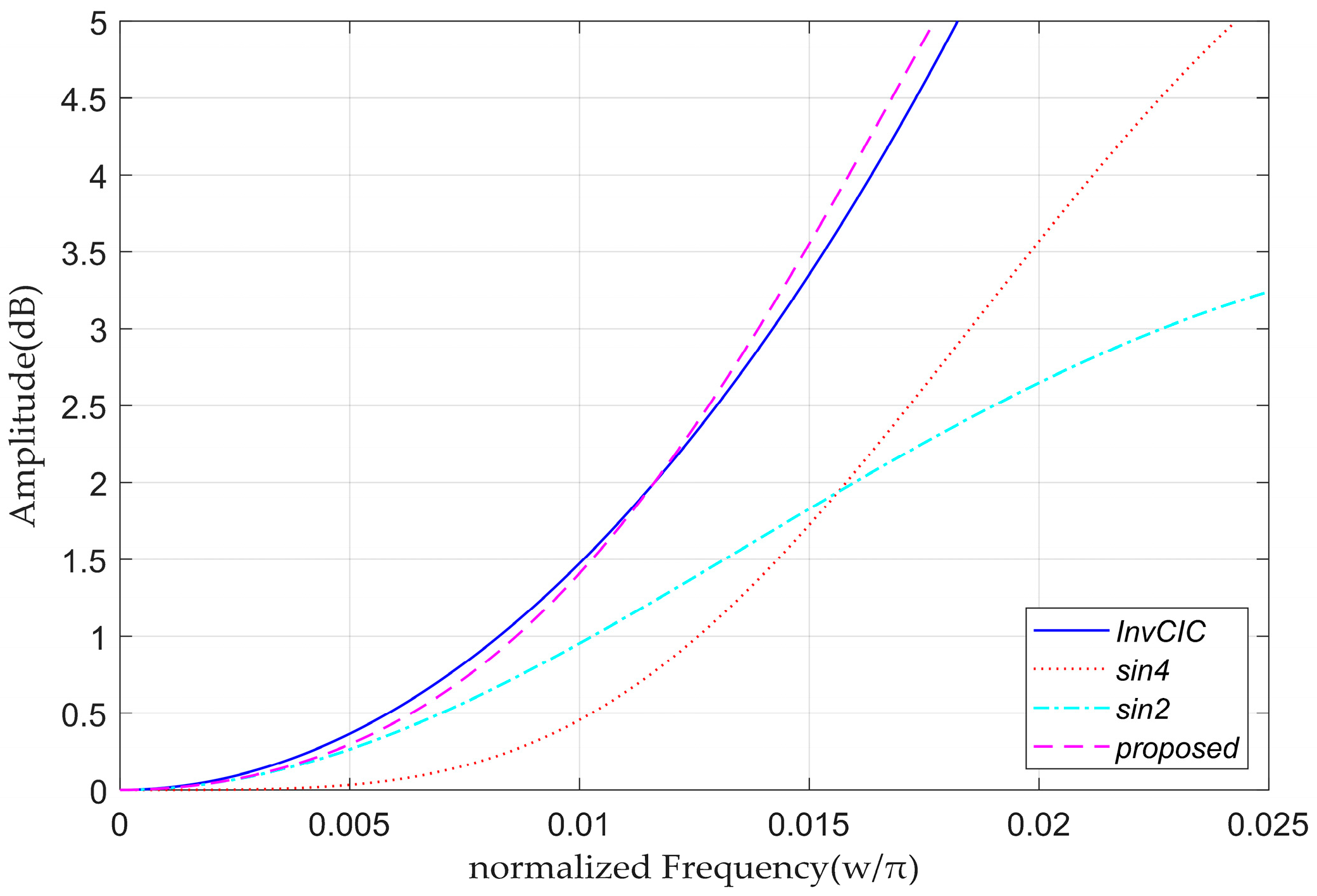
In this section, we adopt a systematic approach to realize the proposed design. The methodology adheres to a three-step framework that begins with modeling and simulation, progresses to FPGA verification, and culminates in ASIC design.

3.1. Simulation

Models for the modulator and digital decimation filter are constructed utilizing the MATLAB R2023b’s Simulink simulation platform. Figure 11 illustrates a single-loop third-order sigma-delta modulator with a feedforward path, employing the DWA technique to mitigate nonlinearity issues in the feedback DAC. The green module represents the DWA module, and the orange module signifies the quantizer within the modulator. Figure 12 depicts the schematic diagram of the complete sigma-delta ADC system model, incorporating the modulator model shown in Figure 11 along with the proposed design.
To verify functional correctness, simulations are conducted using a 781 Hz ideal sine wave as the system input. The resulting waveforms at each stage are shown in Figure 13, arranged from bottom to top as follows: modulator output, CIC filter output, compensation filter output, and half-band filter output. Figure 13 demonstrates that the digital decimation filter successfully reconstructs the sine signal from a high sampling rate to a lower sampling frequency, effectively removing high-frequency noise. Additionally, the output waveform of the decimation filter exhibits a noticeable delay, which is attributable to the filter’s inherent response delay.
To assess the performance of the proposed design, an FFT analysis is performed on the modulator output and filter output, resulting in the signal spectrum shown in Figure 14. The modulator output signal achieved an SNR of 99.95 dB, while the digital filter output signal reached 99.92 dB. The SNR loss is 0.03 dB, which is less than the overall ripple of 0.0477 dB, thereby satisfying the design requirements.

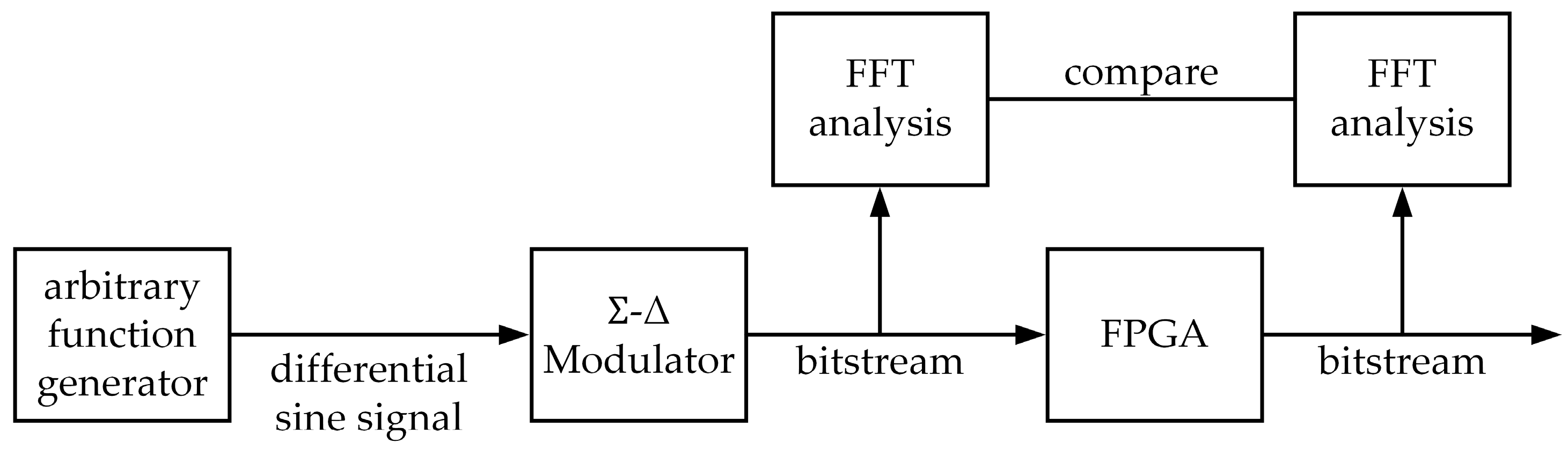
3.2. FPGA Verification

We constructed the test system shown in Figure 15 to validate the proposed design by analyzing and comparing the signals before and after digital downsampling. The main components of this system are a sigma-delta modulator chip test board and an FPGA test board. The architecture of the sigma-delta modulator chip is consistent with the modeling, fabricated using SMIC CMOS 180 nm technology with a voltage of 1.8 V. This chip requires a differential sine signal input [26] with a common-mode level of 0.9 V and outputs a 5-bit quantized bitstream at 2.56 MHz. In this test system, an arbitrary function generator is used to generate the required analog signals, while a logic analyzer synchronously samples and stores the modulator’s output bitstream.
Performing FFT analysis on the obtained bitstream file allows for obtaining the magnitude response of the modulator chip output signal containing high-frequency noise, which is depicted in Figure 16, with an SNR of 91.70 dB.
The FPGA implementation is conducted on a self-developed Xilinx Artix-7 series XC7A35T- 2FTG256 FPGA test board. The synthesis and implementation steps are performed using Vivado 2019.2, and the resource utilization of each module is detailed in Table 3, with total slice LUT resource consumption at 18% (3749/20,800) and total slice register resource consumption at 6% (2497/41,600). After writing the generated bitstream file to the FPGA, the FPGA test board is connected to the modulator chip test board for joint testing. The photograph of the complete test system is shown in Figure 17. The programmable linear DC power supply is employed to power the testing system (with the modulator chip test board powered by 5 V and the FPGA test board by 12 V). To enable real-time data acquisition, the 40 kHz, 24-bit parallel bitstream output from the digital filter is converted to serial data and transmitted to a PC via a serial port at a baud rate of 1.5 Mbps. The processed data is then subjected to FFT analysis, resulting in the signal spectrum shown in Figure 18, with an SNR of 91.66 dB. Table 4 presents the results obtained from testing the input signals across various frequencies. The table shows that the SNR loss after digital decimation filtering is consistently less than 0.04 dB, which meets the design requirements for passband ripple.

3.3. ASIC Design

To assess the ASIC performance of the proposed design for the future implementation of a complete sigma-delta ADC design, the SMIC 180 nm CMOS process is employed to carry out the digital backend flow, which primarily includes logical synthesis and layout design. During the logical synthesis stage, the RTL code of the design is transformed into a gate-level netlist utilizing the design compiler (DC) tool. Subsequently, the encounter tool is employed for layout design, leading to the layout presented in Figure 19, with an area of 0.72 mm2. The distribution of each filter module on the layout is depicted in Figure 19a, while the final layout with metal layer is depicted in Figure 19b. Furthermore, the modulator output signal bit stream file of 781 Hz obtained in the modulator testing phase is utilized as input for the post-simulation of the circuit, resulting in an SNR of 91.69 dB. A power analysis is then conducted using the PrimeTime PX (PTPX) tool, which results in a power consumption of 0.217 mW. Table 5 shows the performance parameters of several decimation filters. The blue module, along with the adjacent pink module above it, represents the CIC filter. The yellow and purple modules signify the compensation filter. The rightmost pink module denotes the half-band filter. The modules that have not been specifically mentioned are designated as other auxiliary components. It can be seen that under the same process and similar performance parameters, the cascade filter structure proposed in this paper achieves lower power consumption.

4. Conclusions

To meet the requirements for high attenuation in the folding band and low passband ripple in digital decimation filters for sigma-delta ADCs, this paper presents a design of a three-stage cascade decimation filter. The filter structure enhances folding band aliasing suppression by inserting an IZ filter into the CIC filter. The second stage compensates the passband attenuation of the CIC filter by using a structure of a fourth- to second-order compensation filter. The third stage employs a half-band filter for efficient two-times downsampling. Based on this architecture, the coefficients of the IZ filter and compensation filter are optimized by using the PSO algorithm. The folding band attenuation and overall passband ripple are 93.4 dB and 0.0477 dB respectively. The filter design is deployed on an FPGA test board and tested with a third-order, 5-bit, sigma-delta modulator chip. The output SNR of the filter reaches 91.7 dB. The ASIC design of the filter is carried out using 180 nm CMOS technology. The layout area is 0.72 mm2, the power consumption is 0.217 mW, and the SNR obtained from the post-layout simulation is 91.7 dB.

Author Contributions

Conceptualization, M.Y. and Z.L.; formal analysis, Y.Z.; investigation, Z.L.; project administration, M.Y. and Y.Z.; resources, M.Y. and Y.Z.; software, Z.L.; supervision, Y.Z.; visualization, Z.L.; writing manuscript, M.Y. and Z.L.; review and editing, M.Y., Z.L. and Y.Z. All authors have read and agreed to the published version of the manuscript.

Funding

This research received no external funding.

Data Availability Statement

Data are contained within the article.

Conflicts of Interest

The authors declare no conflicts of interest.

References

  1. Liu, L.; Li, D.; Ye, Y.; Chen, L.; Wang, Z. A 95dB SNDR audio ΔΣ modulator in 65 nm CMOS. In Proceedings of the 2011 IEEE Custom Integrated Circuits Conference (CICC), San Jose, CA, USA, 19–21 September 2011; pp. 1–4. [Google Scholar]
  2. Zhu, L.; Tong, X. A 1-V 92.28-dB DR Sigma-Delta Modulator for Sensing Applications. In Proceedings of the 2022 7th International Conference on Integrated Circuits and Microsystems (ICICM), Xi’an, China, 28–31 October 2022; pp. 657–661. [Google Scholar]
  3. Qian, Z.B.; Yan, W. Low Resource Consumption Design of Digital Decimation Filter. Acta Sci. Nat. Univ. Pekin. 2018, 54, 315–319. [Google Scholar]
  4. Luo, L.; Li, X.Y.; Zeng, J.Q.; Xu, Z.X. Design of 24-bit Delta-Sigma A/D digital decimation filter. J. Beijing Jiaotong Univ. 2016, 40, 45–49. [Google Scholar]
  5. Li, D.; Chen, Z.; Liu, X.; Shen, Z.; Xing, Y.; Wan, P. Digital Decimation Filter Design for a 3rd-Order Sigma-Delta Modulator with Achieving 129 dB SNR. In Proceedings of the 2021 IEEE 15th International Conference on Anti-counterfeiting, Security, and Identification (ASID), Xiamen, China, 29–31 October 2021; pp. 187–190. [Google Scholar]
  6. Fernandez-Vazquez, A.; Dolecek, G.J. Passband and stopband CIC improvement based on efficient IIR filter structure. In Proceedings of the 2010 53rd IEEE International Midwest Symposium on Circuits and Systems, Seattle, WA, USA, 1–4 August 2010; pp. 765–768. [Google Scholar]
  7. Molnar, G.; Dudarin, A.; Vucic, M. Minimax design of multiplierless sharpened CIC filters based on interval analysis. In Proceedings of the 2016 39th International Convention on Information and Communication Technology, Electronics and Microelectronics (MIPRO), Opatija, Croatia, 30 May–3 June 2016; pp. 94–98. [Google Scholar]
  8. Molnar, G.; Dudarin, A.; Vucic, M. Design and multiplierless realization of maximally flat sharpened-CIC compensators. IEEE Trans. Circuits Syst. II Express Briefs 2017, 65, 51–55. [Google Scholar] [CrossRef]
  9. Gautam, D.; Khare, K.; Shrivastava, B.P. A novel approach for optimal design of sample rate conversion filter using linear optimization technique. IEEE Access 2021, 9, 44436–44441. [Google Scholar] [CrossRef]
  10. Dolecek, G.J.; Dolecek, L. Exploiting features of symmetric polynomials for improved comb filter design. In Proceedings of the 2016 Signal Processing: Algorithms, Architectures, Arrangements, and Applications (SPA), Poznan, Poland, 21–23 September 2016; pp. 26–29. [Google Scholar]
  11. Dolecek, G.J. Design of comb decimation filter with improved aliasing rejection and compensated passband. In Proceedings of the 2021 IEEE 32nd International Conference on Microelectronics (MIEL), Nis, Serbia, 12–14 September 2021; pp. 255–258. [Google Scholar]
  12. Jovanovic Dolecek, G.; Baez, R.G.; Molina Salgado, G.; De La Rosa, J.M. Novel multiplierless wideband comb compensator with high compensation capability. Circuits Syst. Signal Process. 2017, 36, 2031–2049. [Google Scholar] [CrossRef]
  13. Xu, L.; Yang, W.; Tian, H. Design of wideband CIC compensator based on particle swarm optimization. Circuits Syst. Signal Process. 2019, 38, 1833–1846. [Google Scholar] [CrossRef]
  14. Neeraja, P.; Bindiya, T.; Raghu, C. Low Power Implementation of Compensated and Sharpened CIC Decimation Filter. In Proceedings of the 2022 IEEE 9th Uttar Pradesh Section International Conference on Electrical, Electronics and Computer Engineering (UPCON), Prayagraj, India, 2–4 December 2022; pp. 1–6. [Google Scholar]
  15. Cao, J.; Liu, Y.; Jiang, B.; Liu, X. The design and implementation of sigma delta ADC digital decimation filter. In Proceedings of the 2013 International Conference on Information Science and Cloud Computing Companion, Guangzhou, China, 7–8 December 2013; pp. 335–338. [Google Scholar]
  16. Konvalina, J.; Matache, V. Palindrome-polynomials with roots on the unit circle. Comptes Rendus Math. 2004, 26, 39. [Google Scholar]
  17. Botta, V. Some results on zeros of palindromic and perturbed polynomials of even degree. Proceeding Ser. Braz. Soc. Comput. Appl. Math. 2015, 3. [Google Scholar] [CrossRef]
  18. Nadar, N.; Mehta, M.; Bhat, K.; Mendes, J.; Chaudhari, R. Hardware implementation of pipelined FFT using polyphase decomposition. In Proceedings of the 2021 International Conference on Recent Trends on Electronics, Information, Communication & Technology (RTEICT), Bangalore, India, 27–28 August 2021; pp. 339–343. [Google Scholar]
  19. Dolecek, G.J. Improving comb alias rejection by exploiting certain class of palindromic polynomials. In Proceedings of the 2017 European Conference on Circuit Theory and Design (ECCTD), Catania, Italy, 4–6 September 2017; pp. 1–4. [Google Scholar]
  20. Kennedy, J.; Eberhart, R. Particle swarm optimization. In Proceedings of the Proceedings of ICNN’95-international conference on neural networks, Perth, WA, Australia, 27 November–1 December 1995; pp. 1942–1948. [Google Scholar]
  21. Mezura-Montes, E.; Coello, C.A.C. Constraint-handling in nature-inspired numerical optimization: Past, present and future. Swarm Evol. Comput. 2011, 1, 173–194. [Google Scholar] [CrossRef]
  22. Gad, A.G. Particle swarm optimization algorithm and its applications: A systematic review. Arch. Comput. Methods Eng. 2022, 29, 2531–2561. [Google Scholar] [CrossRef]
  23. Dudarin, A.; Molnar, G.; Vucic, M. Optimum multiplierless sharpened cascaded-integrator-comb filters. Digit. Signal Process. 2022, 127, 103564. [Google Scholar] [CrossRef]
  24. Zahradnik, P.; Vlcek, M. Equiripple approximation of half-band FIR filters. IEEE Trans. Circuits Syst. II Express Briefs 2009, 56, 941–945. [Google Scholar] [CrossRef]
  25. Ifeachor, E.C.; Jervis, B.W. Digital Signal Processing: A Practical Approach; Pearson Education: London, UK, 2002. [Google Scholar]
  26. IEEE Std 1241-2023; IEEE Standard for Terminology and Test Methods for Analog-to-Digital Converters. Available online: https://ieeexplore.ieee.org/document/10269815 (accessed on 6 October 2023).
  27. Zhong, Y.Q.; Tian, Y.; Li, J.X.; Liu, M.; Zhang, X.; Meng, Z.; Chen, H.; Yan, Y. Design of Low cost ∑△ ADC digital decimation filter. Microelectron. Comput. 2021, 38, 59–65. [Google Scholar]
Figure 1. Signal downsampling process of digital decimation filter.
Electronics 13 02090 g001
Figure 2. Pole-zero plot of HI(z).
Electronics 13 02090 g002
Figure 3. Magnitude responses of the proposed filter and 4th-order CIC filter.
Electronics 13 02090 g003
Figure 4. Overall structure of proposed CIC filter.
Electronics 13 02090 g004
Figure 5. Magnitude responses of InvCIC, 4th-order/2nd-order and the proposed compensation filter.
Electronics 13 02090 g005
Figure 6. Magnitude response of CIC filter before and after coefficient was optimized.
Electronics 13 02090 g006
Figure 7. Magnitude response of proposed CIC filter before and after compensation, including an enlarged view of passband ripple before and after the SPT solution.
Electronics 13 02090 g007
Figure 8. Magnitude response of half-band filters with different quantization bit widths.
Electronics 13 02090 g008
Figure 9. Magnitude response of proposed cascade decimation filter structure with the consideration of filter coefficient quantization.
Electronics 13 02090 g009
Figure 10. Proposed structure of half-band filter.
Electronics 13 02090 g010
Figure 11. Simulink model of the modulator.
Electronics 13 02090 g011
Figure 12. Simulink model of the sigma-delta ADC system.
Electronics 13 02090 g012
Figure 13. Output signals of the modulator, CIC filter, compensation filter, and half-band filter.
Electronics 13 02090 g013
Figure 14. FFT results. (a) Magnitude response of the modulator model output signal; (b) magnitude response of the decimation filter model output signal.
Electronics 13 02090 g014
Figure 15. Schematic of the test system.
Electronics 13 02090 g015
Figure 16. Magnitude response of modulator output signal.
Electronics 13 02090 g016
Figure 17. Photograph of the modulator–FPGA test system.
Electronics 13 02090 g017
Figure 18. Magnitude response of FPGA output signal.
Electronics 13 02090 g018
Figure 19. Layout of cascade decimation filters. (a) Distribution of decimation filter modules on the layout; (b) layout of decimation filters with metal layer.
Electronics 13 02090 g019
Table 1. Coefficient of full accuracy and coefficient after SPT solution.
Raw CoefficientsSPT SolutionSPT Coefficients
A1 = 1.52651 + 2−1 + 2−6 + 2−7 + 2−8A1s = 1.52734375
A2 = 1.12521 + 2−3A2s = 1.125
Table 2. Magnitude characteristic comparison of similar works.
Ref.[12][8][14]This Work
Decimation factor32323232
Minimum attenuation in dB41.882.57993.4
Maximum passband ripple in dB0.0670.09-0.0469
Table 3. Resource utilization of the hardware of the proposed design.
Modules after Vivado SynthesisSlice LUTsSlice Registers
Top3749 out of 20,8002497 out of 41,600
Clock module6 out of 20,8007 out of 41,600
CIC module1660 out of 20,800968 out of 41,600
4th-order compensation module540 out of 20,800120 out of 41,600
2nd-order compensation module128 out of 20,80063 out of 41,600
Half-band module1415 out of 20,8001339 out of 41,600
Table 4. SNR of multiple frequency signals before and after digital downsampling filtering.
Input signal frequency in Hz 111478110682298473010,223
Modulator output SNR in dB91.6791.7091.4491.4591.2190.68
FPGA output SNR in dB91.6491.6691.4191.4391.1990.65
1 The input signal frequency is selected to meet the requirements of coherent sampling.
Table 5. Comparison of similar works.
Ref.[3][4][27]This Work
Sampling frequency in KHz3072409632002560
Oversampling factor6410246464
Bandwidth in KHz21.622520
SNR in dB87.2154-91.7
Chip technology node in nm130180180180
Area in mm20.14640.40.72
Power in mW1.73205.30.217
Disclaimer/Publisher’s Note: The statements, opinions and data contained in all publications are solely those of the individual author(s) and contributor(s) and not of MDPI and/or the editor(s). MDPI and/or the editor(s) disclaim responsibility for any injury to people or property resulting from any ideas, methods, instructions or products referred to in the content.

