
CMOS IC Solutions for the 77 GHz Radar Sensor in Automotive Applications

 , , , and
Abstract
:1. Introduction
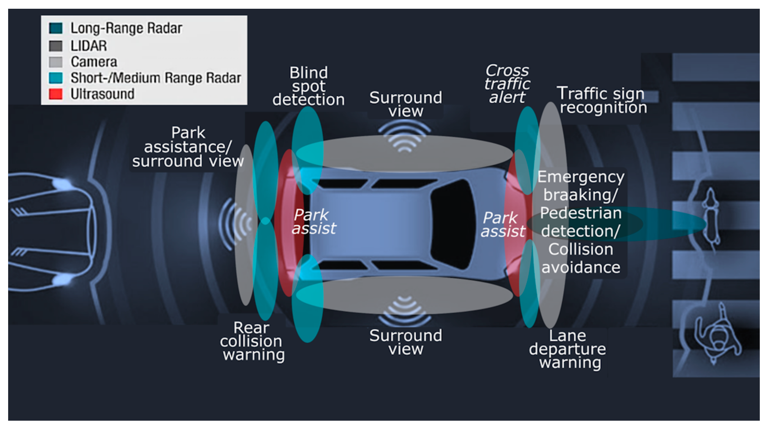
2. System Analysis
3. Overview of 28 nm FD-SOI Technology
4. CMOS ICs for 77 GHz Automotive Radar
4.1. Design of 77 GHz Receiver with TX Leakage Suppression
4.2. Design of 77 GHz Transmitter for Automotive Radar Sensors
4.3. Transformer-Based VCO
5. Conclusions
Author Contributions
Funding
Conflicts of Interest
References
- Kukkala, V.K.; Tunnell, J.; Pasricha, S.; Bradley, T. Advanced driver-assistance systems: A path toward autonomous vehicles. IEEE Consum. Electron. Mag. 2018, 7, 18–25. [Google Scholar] [CrossRef]
- Hung, C.; Lin, A.T.; Peng, B.C.; Wang, H.; Hsu, J.L.; Lu, Y.J.; Hsu, W.; Zhan, J.H.C.; Juan, B.; Lok, C.H.; et al. Toward automotive surround-view radars. In Proceedings of the 2019 IEEE International Solid-State Circuits Conference-(ISSCC), San Francisco, CA, USA, 17–21 February 2019; pp. 162–164. [Google Scholar]
- Chen, L.; Zhang, L.; Wang, Y. A 26.4-dB gain 15.82-dBm 77-GHz CMOS power amplifier with 15.9% PAE using transformer-based quadrature coupler network. IEEE Microw. Wirel. Compon. Lett. 2020, 30, 78–81. [Google Scholar] [CrossRef]
- Pekarik, J.J.; Adkisson, J.; Gray, P.; Liu, Q.; Camillo-Castillo, R.; Khater, M.; Jain, V.; Zetterlund, B.; DiVergilio, A.; Tian, X.; et al. A 90 nm SiGe BiCMOS technology for mm-wave and high-performance analog application. In Proceedings of the IEEE Bipolar/BiCMOS Circuits and Technology Meeting, Coronado, CA, USA, 28 September–1 October 2014; pp. 92–95. [Google Scholar]
- Trotta, S.; Wintermantel, M.; Dixon, J.; Moeller, U.; Jammers, R.; Hauck, T.; Samulak, A.; Dehlink, B.; Shun-Meen, K.; Li, H.; et al. An RCP packaged transceiver chipset for automotive LRR and SRR systems in SiGe BiCMOS technology. IEEE Trans. Microw. Theory Tech. 2012, 60, 778–794. [Google Scholar] [CrossRef]
- Chevalier, P.; Avenier, G.; Ribes, G.; Montagné, A.; Canderle, E.; Céli, D.; Derrier, N.; Deglise, C.; Durand, C.; Quémerais, T.; et al. A 55 nm triple gate oxide 9 metal layers SiGe BiCMOS technology featuring 320 GHz fT/370 GHz fMAX HBT and high Q millimeter-wave passives. In Proceedings of the 2014 IEEE International Electron Devices Meeting, San Francisco, CA, USA, 15–17 December 2014; pp. 3.9.1–3.9.3. [Google Scholar]
- Joseph, A.; Jain, V.; Ong, S.N.; Wolf, R.; Lim, S.F.; Singh, J. Technology positioning for mm-wave applications: 130/90 nm SiGe BiCMOS vs. 28 nm RFCMOS. In Proceedings of the 2018 IEEE BiCMOS and Compound Semiconductor Integrated Circuits and Technology Symposium (BCICTS), San Diego, CA, USA, 15–17 October 2018; pp. 18–21. [Google Scholar]
- Belfiore, F.; Calcagno, A.; Borgonovo, G.; Castro, M.G.; Pisasale, A.; Platania, M.; Vinciguerra, M.; Alessi, G.; Burgio, C.; Leonardi, S.; et al. A 76 to 81GHz packaged transceiver for automotive radar with FMCW modulator and ADC. In Proceedings of the 2017 European Radar Conference (EURAD), Nuremberg, Germany, 11–13 October 2017; pp. 143–146. [Google Scholar]
- Arai, T.; Usugi, T.; Murakami, T.; Kishimoto, S.; Utagawa, Y.; Kohtani, M.; Ando, I.; Matsunaga, K.; Arai, C.; Yamaura, S. A 77-GHz 8RX3TX transceiver for 250-m long-range automotive radar in 40-nm CMOS technology. IEEE J. Solid-State Circuits 2021, 56, 1332–1344. [Google Scholar] [CrossRef]
- Giannini, V.; Goldenberg, M.; Eshraghi, A.; Maligeorgos, J.; Lim, L.; Lobo, R.; Welland, D.; Chow, C.K.; Dornbusch, A.; Dupuis, T.; et al. A 192-virtual-receiver 77/79 GHz GMSK code-domain MIMO radar system-on-chip. In Proceedings of the 2019 IEEE International Solid-State Circuits Conference—(ISSCC), San Francisco, CA, USA, 17–21 February 2019; pp. 164–166. [Google Scholar]
- Ginsburg, B.P.; Subburaj, K.; Samala, S.; Ramasubramanian, K.; Singh, J.; Bhatara, S.; Murali, S.; Breen, D.; Moallem, M.; Dandu, K.; et al. A multimode 76-to-81GHz automotive radar transceiver with autonomous monitoring. In Proceedings of the 2018 IEEE International Solid-State Circuits Conference—(ISSCC), San Francisco, CA, USA, 11–15 February 2018; pp. 158–160. [Google Scholar]
- Cathelin, A. Fully depleted silicon on insulator devices CMOS: The 28-nm node is the perfect technology for analog, RF, mmW, and mixed-signal system-on-chip integration. IEEE Solid-State Circuits Mag. 2017, 9, 18–26. [Google Scholar] [CrossRef]
- Pan, D.; Duan, Z.; Wu, B.; Wang, Y.; Huang, D.; Gui, P.; Sun, L. A digitally controlled CMOS receiver with 14 dBm P1dB for 77 GHz automotive radar. In Proceedings of the 2019 IEEE International Symposium on Circuits and Systems (ISCAS), Sapporo, Japan, 26–29 May 2019; pp. 1–4. [Google Scholar]
- Lou, L.; Tang, K.; Chen, B.; Guo, T.; Wang, Y.; Wang, W.; Fang, Z.; Liu, Z.; Zheng, Y. A 253 mW/channel 4TX/4RX pulsed chirping phased-array radar TRX in 65 nm CMOS for X-band synthetic-aperture radar imaging. In Proceedings of the 2018 IEEE International Solid-State Circuits Conference—(ISSCC), San Francisco, CA, USA, 11–15 February 2018; pp. 160–162. [Google Scholar]
- Avenier, G.A.; Diop, M.; Chevalier, P.; Troillard, G.; Loubet, N.; Bouvier, J.; Depoyan, L.; Derrier, N.; Buczko, M.; Leyris, C.; et al. 0.13 m SiGe BiCMOS technology fully dedicated to mm-wave applications. IEEE J. Solid-State Circuits 2009, 44, 2312–2321. [Google Scholar] [CrossRef]
- Skolnik, M.I. Introduction to Radar Systems; MacGraw-Hill: New York, NY, USA, 2001. [Google Scholar]
- Lee, J.; Li, Y.-A.; Hung, M.-H.; Huang, S.-J. A fully-integrated 77-GHz FMCW radar transceiver in 65-nm CMOS technology. IEEE J. Solid-State Circuits 2010, 45, 2746–2756. [Google Scholar] [CrossRef]
- Australian Communication Authority. A Review of Automotive Radar Systems-Devices and Regulatory Frameworks; Document SP 4/01; Australian Communication Authority: Canberra, Austra, 2001.
- Medra, A.; Guermandi, D.; Vaesen, K.; Brebels, S.; Bourdoux, A.; Van Thillo, W.; Wambacq, P.; Giannini, V. An 80 GHz low-noise amplifier resilient to the TX spillover in phase-modulated continuous-wave radars. IEEE J. Solid-State Circuits 2016, 51, 1141–1153. [Google Scholar] [CrossRef]
- Lin, K.; Wang, Y.E.; Pao, C.-K.; Shih, Y.-C. A Ka-band FMCW radar front-end with adaptive leakage cancellation. IEEE Microw. Theory Tech. 2006, 54, 4041–4048. [Google Scholar] [CrossRef]
- Papotto, G.; Nocera, C.; Finocchiaro, A.; Parisi, A.; Cavarra, A.; Castorina, A.; Ragonese, E.; Palmisano, G. A 27-mW W-band radar receiver with effective TX leakage suppression in 28-nm FD-SOI CMOS. IEEE Trans. Microw. Theory Tech. 2021, 69, 4132–4141. [Google Scholar] [CrossRef]
- Papotto, G.; Parisi, A.; Finocchiaro, A.; Nocera, C.; Cavarra, A.; Castorina, A.; Palmisano, G. A W-Band Transmitter for Automotive Radar Sensors in 28-nm FD-SOI CMOS. IEEE Trans. Microw. Theory Tech. 2023, 71, 4577–4587. [Google Scholar] [CrossRef]
- Jia, H.; Kuang, L.; Zhu, W.; Wang, Z.; Ma, F.; Wang, Z.; Chi, B. A 77 GHz frequency doubling two-path phased-array FMCW transceiver for automotive radar. IEEE J. Solid-State Circuits 2016, 51, 2299–2311. [Google Scholar] [CrossRef]
- Hsiao, R.Y.H.; Chang, Y.C.; Tsai, C.H.; Huang, T.Y.; Aloui, S.; Huang, D.J.; Chen, Y.H.; Tsai, P.H.; Kao, J.C.; Lin, Y.H.; et al. A 77-GHZ 2T6R transceiver with injection-lock frequency sextupler using 65-nm CMOS for automotive radar system application. IEEE Trans. Microw. Theory Tech. 2016, 64, 3031–3048. [Google Scholar] [CrossRef]
- Texas Instruments. 76-GHz to 81-GHz High-Performance Automotive MMIC. May 2017. Available online: https://www.ti.com/product/AWR1243 (accessed on 23 May 2024).
- Carter, R.; Mazurier, J.; Pirro, L.; Sachse, J.U.; Baars, P.; Faul, J.; Grass, C.; Grasshoff, G.; Javorka, P.; Kammler, T.; et al. 22 nm FDSOI technology for emerging mobile, Internet-of-Things, and RF applications. In Proceedings of the 2016 IEEE International Electron Devices Meeting (IEDM), San Francisco, CA, USA, 3–7 December 2016; pp. 2.2.1–2.2.4. [Google Scholar]
- Nocera, C.; Cavarra, A.; Ragonese, E.; Papotto, G.; Palmisano, G. Down-converter solutions for 77-GHz automotive radar sensors in 28-nm FD-SOI CMOS technology. In Proceedings of the 2018 14th Conference on Ph.D. Research in Microelectronics and Electronics (PRIME), Prague, Czech Republic, 2–5 July 2018; pp. 153–156. [Google Scholar]
- Gomez, R.; Dutto, C.; Huard, V.; Clerc, S.; Bano, E.; Flatresse, P. Design methodology with body bias: From circuit to engineering. In Proceedings of the 2017 IEEE SOI-3D-Subthreshold Microelectronics Technology Unified Conference (S3S), Burlingame, CA, USA, 16–19 October 2017; pp. 1–4. [Google Scholar]
- Ragonese, E.; Papotto, G.; Nocera, C.; Cavarra, A.; Palmisano, G. CMOS Automotive Radar Sensors: mm-Wave Circuit Design Challenges. IEEE Trans. Circuits Syst. II Express Briefs 2022, 69, 2610–2616. [Google Scholar] [CrossRef]
- de Streel, G.; Stas, F.; Gurne, T.; Durant, F.; Frenkel, C.; Cathelin, A.; Bol, D. SleepTalker: A ULV 802.15.4a IR-UWB transmitter SoC in 28-nm FDSOI achieving 14 pJ/b at 27 Mb/s with channel selection based on adaptive FBB and digitally programmable pulse shaping. IEEE J. Solid-State Circuits 2017, 52, 1163–1177. [Google Scholar] [CrossRef]
- Mroszczyk, P.; Goodacre, J.; Pavlidis, V.F. Energy efficient flash ADC with PVT variability compensation through advanced body biasing. IEEE Trans. Circuits Syst. II Exp. Briefs 2019, 66, 1775–1779. [Google Scholar] [CrossRef]
- Böck, J.; Aufinger, K.; Boguth, S.; Dahl, C.; Knapp, H.; Liebl, W.; Manger, D.; Meister, T.F.; Pribil, A.; Wursthorn, J.; et al. SiGe HBT and BiCMOS process integration optimization within the DOTSEVEN project. In Proceedings of the IEEE Bipolar/BiCMOS Circuits and Technology Meeting, Boston, MA, USA, 26–28 October 2015; pp. 121–124. [Google Scholar]
- Cavarra, A.; Nocera, C.; Papotto, G.; Ragonese, E.; Palmisano, G. Transformer design for 77-GHz down-converter in 28-nm FD-SOI CMOS technology. In Applications in Electronics Pervading Industry, Environment and Society, Proceedings of the ApplePies 2018, Pisa, Italy, 26–27 September 2018; (Lecture Notes in Electrical Engineering); Springer: Cham, Switzerland, 2019; Volume 550, pp. 195–201. [Google Scholar]
- Spataro, S.; Salerno, N.; Papotto, G.; Ragonese, E. The effect of a metal PGS on the Q-factor of spiral inductors for RF and mm-wave applications. in a 28-nm CMOS technology. Wiley Int. J. RF Microw. Comput.-Aided Eng. 2020, 30, e223682. [Google Scholar] [CrossRef]
- Duan, Z.; Wu, B.; Wang, Y.; Fang, Y.; Li, Y.; Wu, Y.; Zhang, T.; Zhu, C.; Dai, Y.; Sang, L.; et al. A 76–81 GHz 2×8 MIMO Radar Transceiver with Broadband Fast Chirp Generation and 16-Antenna-in-Package Virtual Array. IEEE J. Solid-State Circuits 2023, 58, 3103–3112. [Google Scholar] [CrossRef]
- Park, J.; Ryu, H.; Ha, K.-W.; Kim, J.-G.; Baek, D. 76–81-GHz CMOS Transmitter with a Phase-Locked-Loop-Based Multichirp Modulator for Automotive Radar. IEEE Trans. Microw. Theory Tech. 2015, 63, 1399–1408. [Google Scholar] [CrossRef]
- Papotto, G.; Ragonese, E.; Nocera, C.; Finocchiaro, A.; Palmisano, G. Interference-Canceling RF Receiver Circuit, Corresponding System, radar Sensor System, Vehicle and Method. U.S. Patent US-11442142-B2, 12 September 2022. [Google Scholar]
- Nguyen, T.-K.; Kim, C.-H.; Ihm, G.-J.; Yang, M.-S.; Lee, S.-G. CMOS low-noise amplifier design optimization techniques. IEEE Trans. Microw. Theory Tech. 2004, 52, 1433–1442. [Google Scholar] [CrossRef]
- Finocchiaro, A.; Papotto, G.; Ragonese, E.; Palmisano, G. A 28-nm FD-SOI CMOS Variable-Gain Amplifier with Body-Bias-Based DC-Offset Cancellation for Automotive Radars. IEEE Trans. Circuits Syst. II Express Briefs 2019, 66, 1693–1697. [Google Scholar] [CrossRef]
- Parisi, A.; Papotto, G.; Ragonese, E.; Palmisano, G. A 1-V 7th-Order SC Low-Pass Filter for 77-GHz Automotive Radar in 28-nm FD-SOI CMOS. Electronics 2021, 10, 1466. [Google Scholar] [CrossRef]
- Nocera, C.; Papotto, G.; Palmisano, G. Two-Path 77-GHz PA in 28-nm FD-SOI CMOS for Automotive Radar Applications. Electronics 2022, 11, 1289. [Google Scholar] [CrossRef]
- Nocera, C.; Papotto, G.; Cavarra, A.; Ragonese, E.; Palmisano, G. A 13.5-dBm 1-V power amplifier for W-band automotive radar applications in 28-nm FD-SOI CMOS technology. IEEE Trans. Microw. Theory Tech. 2021, 69, 1654–1660. [Google Scholar] [CrossRef]
- Issakov, V.; Rimmelspacher, J.; Trotta, S.; Tiebout, M.; Hagelauer, A.; Weigel, R. A 52-to-67 GHz dual core push push VCO in 40-nm CMOS. Int. J. Microw. Wirless Technol. 2018, 14, 783–793. [Google Scholar] [CrossRef]
- Papotto, G.; Cavarra, A.; Palmisano, G. Frequency Multiplier Circuitry, Corresponding System and Vehicle. U.S. Patent Appl. 17838159, 10 June 2022. [Google Scholar]
- Song, J.; Cui, C.; Kim, S.; Kim, B.; Nam, S. A low-phase-noise 77-GHz FMCW radar transmitter with a 12.8-GHz PLL and a ×6 frequency multiplier. IEEE Microw. Wirel. Compon. Lett. 2016, 26, 540–542. [Google Scholar] [CrossRef]
- Chen, B.; Luo, W.; Wang, F.; Lin, Y.; Yan, N.; Xu, H. A 22.5-31.2-GHz continuously tuning frequency synthesizer with 8.7-GHz chirp for FMCW applications. IEEE Microw. Wirel. Compon. Lett. 2020, 30, 904–907. [Google Scholar] [CrossRef]
- Szilagyi, L.; Li, S.; Xu, X.; Testa, P.V.; Seidel, A.; Carta, C.; Ellinger, F. 37.2-to-42.0 GHz VCO with −93.4 dBc/Hz Phase Noise for FMCW Radar in 22 nm FDSOI. In Proceedings of the 16th European Microwave Integrated Circuits Conference (EuMIC), London, UK, 3–4 April 2022; pp. 221–224. [Google Scholar]
- Levantino, S.; Samori, C.; Zanchi, A.; Lacaita, A.L. AM-to-PM conversion in varactor-tuned oscillators. IEEE Trans. Circuits Syst. II Analog Digit. Signal Process. 2002, 49, 509–513. [Google Scholar] [CrossRef]
- Liu, X.; Luong, H.C. Analysis and Design of Magnetically Tuned W-Band Oscillators. IEEE Trans. Very Large Scale Integr. (VLSI) Syst. 2022, 30, 732–743. [Google Scholar] [CrossRef]
- Basaligheh, A.; Saffari, P.; Winkler, W.; Moez, K. A wide tuning range, low phase noise, and area efficient dual-band milli-meterwave CMOS VCO based on switching cores. IEEE Trans. Circuits Syst. I Reg. Pap. 2019, 66, 2888–2897. [Google Scholar] [CrossRef]
- Papotto, G.; Parisi, A.; Cavarra, A.; Palmisano, G. Voltage-Controlled Oscillator and Method for Using the Same. U.S. Patent US11689156-B1, 27 June 2023. [Google Scholar]
- Kuo, Y.-H.; Tsai, J.-H.; Huang, T.W. A 1.7-mW, 16.8% frequency tuning, 24-GHz transformer-based LC-VCO using 0.18-µm CMOS technology. In Proceedings of the 2009 IEEE Radio Frequency Integrated Circuits Symposium, Boston, MA, USA, 7–9 June 2009; pp. 79–82. [Google Scholar]
- Cavarra, A.; Papotto, G.; Parisi, A.; Finocchiaro, A.; Nocera, C.; Palmisano, G. Transformer-based VCO for W-band automotive radar applications. Electronics 2021, 10, 531. [Google Scholar] [CrossRef]


| [23] | [24] | [25] | This Work | |
|---|---|---|---|---|
| Technology | 65 nm CMOS | 65 nm CMOS | 45 nm CMOS | 28 nm SOI CMOS |
| Architecture | LNA-MIXER-VGA-LPF | LNA-MIXER | LNA-MIXER-VGA-LPF | MIXER-VGA-LPF |
| Operating frequency [GHz] | 77 | 77 | 77 | 77 |
| Power supply [V] | 1 (Down-converter) 1.2 (IF Baseband) | 1 | 1.3 (Down-converter) 1.8 (IF Baseband) | 1 |
| Power consumption [mW] | 30 (a) | 60 | - | 27 (a)(b) |
| Max gain [dB] | 101 | 32 | 48 | 75 |
| Gain variation [dB] | 53 | - | 24 | 42 |
| Gain step [dB] | 6 | - | 2 | 3 |
| IF bandwidth | 5 MHz | 300 MHz | 175 kHz ÷ 15 MHz | 50 kHz ÷ 20 MHz |
| Noise figure [dB] | 8 (@3 MHz) | 5.8 (@10 MHz) | 14 (@1 MHz) | 10.5 (@1 MHz) 8.2 (@10 MHz) |
| OP1dB [dBV] | - | −16 (IP1dB = −37 dBm) | −9 (IP1dB = −22 dBm) | −1.5 (IP1dB = −23.5 dBm) |
| Blocker immunity [dBm] | - | - | −8 | −9.5 |
| Reference | Technology | Features | Pout [dBm] | Pdc [mW] | Psat/Pdc [%] |
|---|---|---|---|---|---|
| [2] | 65 nm CMOS | 1-TX 1-RX | 13 | - | - |
| [9] | 40 nm CMOS | 3-TX 8-RX | 14.1 | - | - |
| [23] | 65 nm CMOS | 1-TX 1-RX | 13 | 175 | 11.4 |
| [24] | 65 nm CMOS | 2-TX 6-RX | 13.7 | 381 | 6 |
| [45] | 65 nm CMOS | 1-TX | 8.9 | 117 (1) | 6.8 |
| This work | 28 nm CMOS | 1-TX | 17.5 | 336 | 16.7 |
Disclaimer/Publisher’s Note: The statements, opinions and data contained in all publications are solely those of the individual author(s) and contributor(s) and not of MDPI and/or the editor(s). MDPI and/or the editor(s) disclaim responsibility for any injury to people or property resulting from any ideas, methods, instructions or products referred to in the content. |
© 2024 by the authors. Licensee MDPI, Basel, Switzerland. This article is an open access article distributed under the terms and conditions of the Creative Commons Attribution (CC BY) license (https://creativecommons.org/licenses/by/4.0/).
Share and Cite
Papotto, G.; Parisi, A.; Finocchiaro, A.; Nocera, C.; Cavarra, A.; Castorina, A.; Palmisano, G. CMOS IC Solutions for the 77 GHz Radar Sensor in Automotive Applications. Electronics 2024, 13, 2104. https://doi.org/10.3390/electronics13112104
Papotto G, Parisi A, Finocchiaro A, Nocera C, Cavarra A, Castorina A, Palmisano G. CMOS IC Solutions for the 77 GHz Radar Sensor in Automotive Applications. Electronics. 2024; 13(11):2104. https://doi.org/10.3390/electronics13112104
Chicago/Turabian StylePapotto, Giuseppe, Alessandro Parisi, Alessandro Finocchiaro, Claudio Nocera, Andrea Cavarra, Alessandro Castorina, and Giuseppe Palmisano. 2024. "CMOS IC Solutions for the 77 GHz Radar Sensor in Automotive Applications" Electronics 13, no. 11: 2104. https://doi.org/10.3390/electronics13112104
APA StylePapotto, G., Parisi, A., Finocchiaro, A., Nocera, C., Cavarra, A., Castorina, A., & Palmisano, G. (2024). CMOS IC Solutions for the 77 GHz Radar Sensor in Automotive Applications. Electronics, 13(11), 2104. https://doi.org/10.3390/electronics13112104