Article

Investigation of Hydrogen Flux Influence on InGaP Layer and Device Uniformity

1
Key Laboratory of Semiconductor Materials Science, Institute of Semiconductors, Chinese Academy of Sciences, Beijing 100083, China
2
College of Materials Science and Opto-Electronic Technology, University of Chinese Academy of Sciences, Beijing 100049, China
3
Beijing Key Laboratory of Low Dimensional Semiconductor Materials and Devices, Beijing 100083, China
*
Authors to whom correspondence should be addressed.
Electronics 2024, 13(11), 2109; https://doi.org/10.3390/electronics13112109
Submission received: 1 April 2024 / Revised: 23 May 2024 / Accepted: 27 May 2024 / Published: 29 May 2024

Abstract

:
In this study, we conduct a comprehensive examination of the influence of hydrogen (H2) carrier gas flux on the uniformity of epitaxial layers, specifically focusing on the InGaP single layer and the full structure of the InGaP/GaAs heterojunction bipolar transistor (HBT). The results show that an elevated flux of H2 carrier gas markedly facilitates the stabilization of layer uniformity. Optimal uniformity in epitaxial wafers is achievable at a suitable carrier gas flux. Furthermore, this study reveals a significant correlation between the uniformity of the InGaP single layer and the overall uniformity of HBT structures, indicating a consequential interdependence.

1. Introduction

III–V alloy semiconductors, known for their unique direct bandgap and superior electron mobility over silicon, have gained significant attention in optoelectronics and microelectronics. Their direct bandgap minimizes energy loss in photoelectronic conversion, enhancing efficiency. Moreover, their high electron drift rates enable faster electron transfer, which facilitates high speed in microelectronic devices [1,2,3,4,5]. Among these, InGaP stands out for its exceptional physical attributes. It not only has the advantages of direct bandgap for efficient photoelectronic conversion but also has remarkable electron mobility and stability. Additionally, the epitaxial growth conditions of InGaP influence its ordering and, consequently, its bandgap and other properties, expanding the possibilities of its application. These features render InGaP a versatile material in optoelectronics, including solar cells and detectors, and in high-frequency electronics like high-speed integrated circuits and microwave devices, offering vast application prospects [6,7,8,9,10,11,12,13,14,15]. In the field of heterojunction structures, InGaP/GaAs heterojunctions hold significant advantages over the traditional AlGaAs/GaAs heterojunctions. These benefits are due to the InGaP/GaAs heterojunction’s larger valence band offset and smaller conduction band offset, which collectively enhance current gain and device performance. In InGaP materials, the DX center is the complex of donor and defect. The formation of DX centers is significantly suppressed owing to the absence of aluminum (Al) and the low reactivity of indium (In). This reduction in DX centers markedly enhances the device’s reliability and stability. Moreover, InGaP/GaAs heterojunctions offer lower interfacial recombination rates and superior temperature stability, ensuring consistent performance in varied operating conditions. Beyond these physical properties, InGaP/GaAs heterojunctions excel in fabrication processes. Their high selectivity in etching allows for precise control over material morphology and structure. The heterojunction’s broad process tolerance ensures stable performance across different fabrication conditions. Coupled with high yields and a manufacturing process, these attributes facilitate large-scale production and applications, positioning InGaP/GaAs heterojunctions as a formidable choice in advanced semiconductor technologies [16,17,18,19,20,21,22,23,24,25,26]. The integration of large-size epitaxial wafers into semiconductor manufacturing significantly enhances production efficiency and material usage, thereby reducing the cost per unit area. In the fundamental current industrial landscape, which emphasizes high efficiency and cost-effectiveness, the adoption of large-size wafers is crucial. They not only streamline production but also minimize material waste across various processing stages, leading to substantial cost savings. Yet, the shift towards larger wafers introduces complexities in maintaining epitaxial uniformity. The expansion of wafer size complicates control over temperature gradients, gas flux, and reaction rates during epitaxy, potentially resulting in uneven thickness, composition, and crystal structure across the wafer. This variability can compromise product stability. To address these challenges, the development of advanced epitaxial techniques that ensure consistent high-quality growth on large wafers is a key focus in semiconductor research, underscoring its significance for future manufacturing innovations [27,28]. The study of large-sized InGaP and In0.49Ga0.51P/GaAs heterojunction bipolar transistor (HBT) epitaxial processes is therefore of fundamental importance. During the epitaxial growth of InGaP, achieving high-quality layers demands precise control over the experimental conditions, notably within a temperature range governed by mass transport. This specific range is favored because it minimizes external influences on the growth process. Here, the kinetics of epitaxial growth rely on the diffusion rate of reactants to the surface, making the growth rate independent of temperature fluctuations. This independence is crucial as it grants researchers the ability to finely adjust the process, specifically through the modulation of the flux and concentration of group III sources. Such adjustments enable the precise tuning of the growth rate, optimizing the epitaxial layer’s thickness, composition, and crystal structure, thereby enhancing the material’s overall quality. Furthermore, within this same temperature bracket, the growth rate can be effectively estimated through a straightforward boundary layer model, encapsulated by the following equation:
r g = C 0 P TMGa v / P 1 / 2
Here, C 0 represents a constant and P TMGa denotes the absolute partial pressure of TMGa, which is entirely depleted at the interface in the gas input stream. Additionally, v symbolizes the gas flux, while P refers to the system’s overall pressure. The aforementioned equations demonstrate that, at a constant growth pressure, the gas flux markedly affects the growth rate, which in turn critically influences the uniformity of the epitaxial wafer [29,30,31].
This study is governed by the gas flux, which is modulated by the total hydrogen (H2) carrier gas flux. Our research primarily targets the application of InGaP HBTs, with a specific emphasis on assessing the electrical uniformity of InGaP. This attribute is crucial for semiconductor performance, underpinning device stability and reliability. We evaluate the electrical uniformity of InGaP through the measurements of sheet resistance uniformity. Sheet resistance, a key indicator of material conductivity, serves as a direct measure of the epitaxial layer’s electrical stability and consistency. This approach allows us to quantify and ensure the performance criteria critical to the operational efficacy of InGaP HBTs.

2. Materials and Methods

This paper investigates the influence of the total H2 carrier gas flux on the epitaxial growth of the InGaP single layer and InGaP/GaAs HBT, using a uniform growth pressure of 25 mbar. We meticulously controlled the growth temperature, V/III ratio, and type and flux of source materials to guarantee the precision and reliability of our findings. Specifically, for the InGaP layer growth, we maintained the temperature at 650 °C and set the V/III ratio to 80, using trimethylgallium (TMGa) and trimethylindium (TMIn) as group III sources and arsenic hydride (AsH3) and phosphine hydride (PH3) as group V sources. Silicon hydride (SiH4) and carbon (C) were introduced as n-type and p-type dopants, respectively. All experiments were conducted on standard 6-inch GaAs substrates with a consistent growth duration of 1000 s. For HBT fabrication, common process and epitaxial wafers were used; the doping concentrations in the InGaAs cap and base regions exceeded 1 × 1019 cm−3, while the InGaP emitter region utilized a lower doping concentration of 1 × 1017 cm−3. In addition, the InGaP collector and semi-collector regions used doping concentrations of 1 × 1017 cm−3and 1 × 1018 cm−3, respectively. To assess the impact of various H2 carrier gas fluxes on epitaxial growth, we carried out a sequence of experiments across different fluxes, followed by an exhaustive characterization and analysis of the epitaxial wafers produced. A warm-wall reactor was used for epitaxial growth. Sheet resistance uniformity, a critical quality metric of the epitaxial wafer, was measured using sheet resistance measurement equipment (LEI-1510EC, Semilab, Budapest, Hungary) across 55 uniformly distributed measurement points on each 6-inch wafer. Furthermore, X-ray diffraction (XRD, PANatical X’Pert3MRD XL, Malvern Panalytical, Malvern, UK) measurement fitting provided thickness data, offering invaluable insights into the growth rate of the epitaxial layers. Direct current (DC) HBT devices were characterized using a semiconductor device parameter analyzer (B1505A, Keysight Technologies, Santa Rosa, CA, USA).

3. Results and Discussion

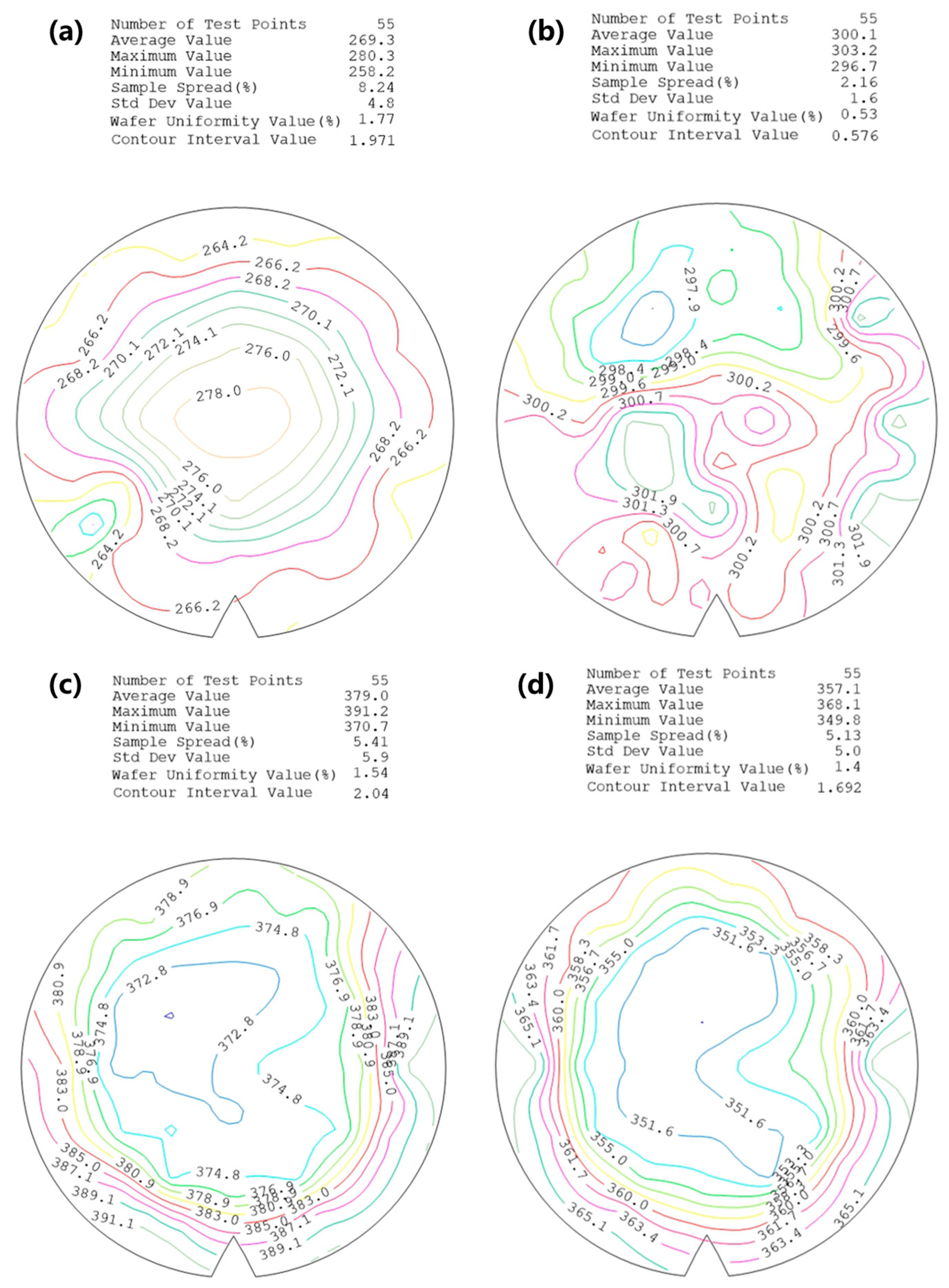
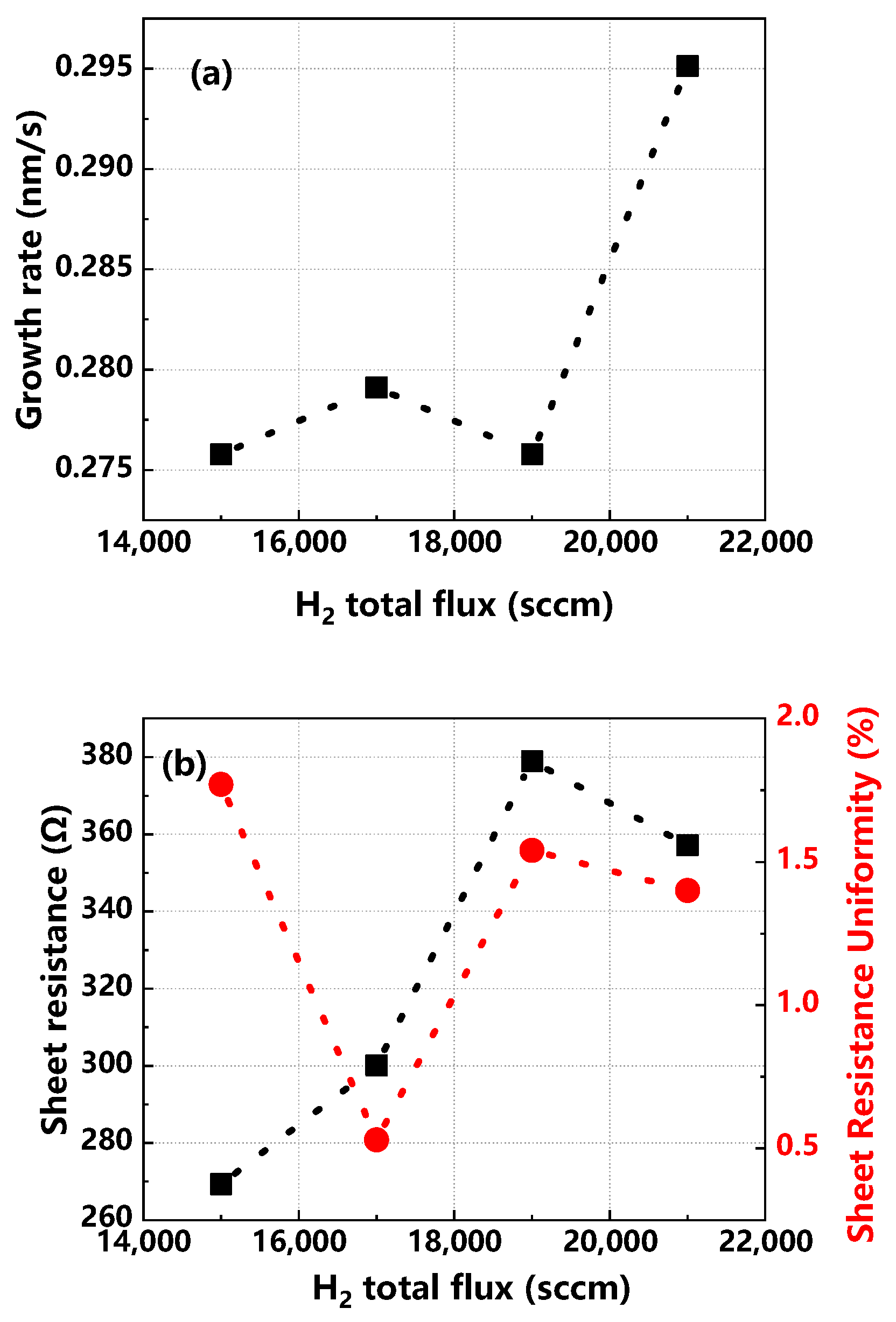
3.1. Influence of Total H2 Flux on the Uniformity of the InGaP Single Layer

In our research, we meticulously designed and executed a series of experiments to thoroughly examine the impact of varying H2 carrier gas fluxes on the electrical uniformity of InGaP epitaxial wafers. Given the critical role of carrier gas flux in determining the quality of epitaxial layer growth during the fabrication of semiconductor materials, understanding its effects is fundamental for material optimization and enhancing device dependability. Our experimental focus was on two primary growth parameters: the growth temperature and the V/III ratio. These parameters are instrumental in influencing the epitaxial layer’s crystal structure, uniformity, components, and doping levels. By setting the growth temperature and V/III ratio to 650 °C and 80, respectively, we aimed to isolate and assess the influence of H2 carrier gas flux variations on the epitaxial wafer’s electrical uniformity within a controlled and stable experimental framework.
To thoroughly investigate how varying H2 carrier gas fluxes affect epitaxial wafer performance, we selected four distinct fluxes for our study: 15,000 sccm, 17,000 sccm, 19,000 sccm, and 21,000 sccm. This range enabled us to observe the impact of H2 carrier gas flux variations on the uniformity of the epitaxial wafers effectively. Our experimental approach adhered strictly to the standard procedures for epitaxial wafer growth, ensuring uniform growth conditions across all samples. The specific growth parameters for each sample are detailed in Table 1. Sample-a to Sample-d correspond to H2 carrier gas flow rates of 21,000 sccm to 15,000 sccm, respectively. By evaluating the performance of these samples under identical measurement conditions, we were able to conduct a detailed analysis of how the total H2 carrier flux influences the electrical uniformity of InGaP epitaxial wafers. The insights gained from this analysis are instrumental in refining the epitaxial growth process and enhancing device performance.
Figure 1 presents the sheet resistance measurements for the InGaP epitaxial layers, observed under varying H2 fluxes. Figure 1a–d corresponds to the sheet resistance test results of Sample-a–Sample-d. As can be seen in Figure 1, Sample-b has the best sheet resistance uniformity, at 0.53%. Figure 2 illustrates the influence of H2 flux on the growth rate, sheet resistance, and uniformity of sheet resistance in InGaP.
Figure 2a demonstrates that with an increase in total H2 flux, there is generally an upward trend in growth rate, except for a notable dip at 19,000 sccm. This decrease is followed by a significant rise as the H2 flux progresses from 19,000 sccm to 21,000 sccm. The primary cause of this pattern is that a higher H2 flux enhances the delivery of growth precursors through the chamber, thereby accelerating the growth rate. However, this trend diverges from predictions made by the simple boundary layer model. A plausible explanation for this anomaly is the premature depletion of TMIn during InGaP’s epitaxial growth as TMGa and TMIn are introduced. As the total H2 flux increases, both TMGa and TMIn are expected to rise proportionately, exacerbating TMIn’s early depletion and, consequently, impacting the growth rate increase. While the simple boundary layer model does not fully account for the total H2 flux impact on growth rate, it does shed light on certain trends observed.
Figure 2b illustrates how variations in total H2 flux impact the sheet resistance of InGaP epitaxial wafers. The graph shows an initial increase in sheet resistance as H2 flux rises, followed by a slight decrease after a certain point. This trend can be attributed to the suppression of side reactions with increasing H2 flux, enhancing gas convection and diffusion within the growth chamber. These improved gas dynamics lead to more uniform reactant distribution on the substrate surface, minimizing concentration gradient-induced side reactions. Consequently, the pathway for unintentional dopants to be incorporated into the epitaxial layer is shortened, reducing unintended doping and, thus, increasing the sheet resistance of the layer. However, once the H2 flux reaches a specific threshold, further reductions in unintentional doping cease to be significant, leading to a stabilization in the rise of sheet resistance. Additionally, the intrinsic N-type character of InGaP may play a role; increased H2 flux leads to a lower V/III ratio on the substrate surface, thus diminishing available group III element sites. This effectively hampers the incorporation of N-type dopants, thereby elevating the sheet resistance of the epitaxial layer.
Figure 2b elucidates not only the effect of total H2 flux on the sheet resistance of epitaxial wafers but also its crucial impact on resistance uniformity. Sheet resistance uniformity, a vital metric for assessing epitaxial wafer performance stability, offers valuable insights for refining the growth process and boosting device quality. The data indicate that sheet resistance uniformity undergoes a nuanced evolution with increasing H2 flux, initially improving and then worsening before finally stabilizing. An initial enhancement in uniformity with moderate increases in H2 flux suggests better mixing and diffusion of source gases within the growth chamber, facilitating more consistent epitaxial growth. However, as H2 flux continues to rise, uniformity begins to diminish, possibly due to growth instabilities triggered by excessive flux, such as source gas concentration fluctuations or growth rate alterations, adversely impacting layer uniformity. Remarkably, at a H2 flux of 19,000 sccm, sheet resistance uniformity peaks at an optimum of 0.53%, indicating that an optimal H2 flux can lead to uniform epitaxial layer growth, laying the groundwork for devices with reliable performance. Furthermore, the impact of the H2 flux rate on uniformity exhibits distinct behaviors across different flux ranges. Below 19,000 sccm, sheet resistance uniformity varies more dramatically with flux changes, highlighting the flux’s pronounced effect on the growth process within this spectrum. Beyond 19,000 sccm, however, uniformity variation with flux diminishes and shows signs of improvement with further increases, suggesting that a higher flux stabilizes gas flow and mixing within the chamber, thereby minimizing growth inhomogeneities.
Our systematic investigation has unequivocally demonstrated the critical impact of total H2 flux on the uniformity of InGaP single-layer epitaxial wafers, underscoring it as a pivotal parameter in the epitaxial growth process. The experiments suggest that optimal H2 flux conditions are essential for achieving highly uniform epitaxial wafers. This conclusion is grounded in two main observations. First, at a constant chamber pressure, increasing H2 flux as a carrier gas enhances the substrate surface’s gas flow rate. This boost not only facilitates the transport of more growth precursors across the substrate but also ensures the timely removal of byproducts, thereby curtailing side reactions that could compromise epitaxial purity and uniformity. Second, uniform distribution of growth sources across the substrate, especially between its center and edges, is crucial for uniform epitaxial growth. A higher H2 flux enhances this distribution, mitigating the impact of gas-phase precursors’ depletion on layer uniformity. However, an excessively high H2 flux may lead to underutilized growth precursors and alter the V/III ratio due to the differential decomposition rates of V sources, affecting the epitaxial layer’s structural and electrical characteristics negatively. Therefore, optimizing the H2 flux, alongside other parameters like growth temperature and V/III ratio, is fundamental for producing high-quality, uniform InGaP epitaxial wafers. This study not only lays a solid experimental foundation but also provides theoretical insights for refining the InGaP epitaxial growth process, offering valuable guidance for the fabrication of superior InGaP-based electronic devices. Future research will delve further into the interplay between H2 flux and other growth parameters, aiming for a more precise and efficient epitaxial growth methodology [32,33,34,35,36,37,38].

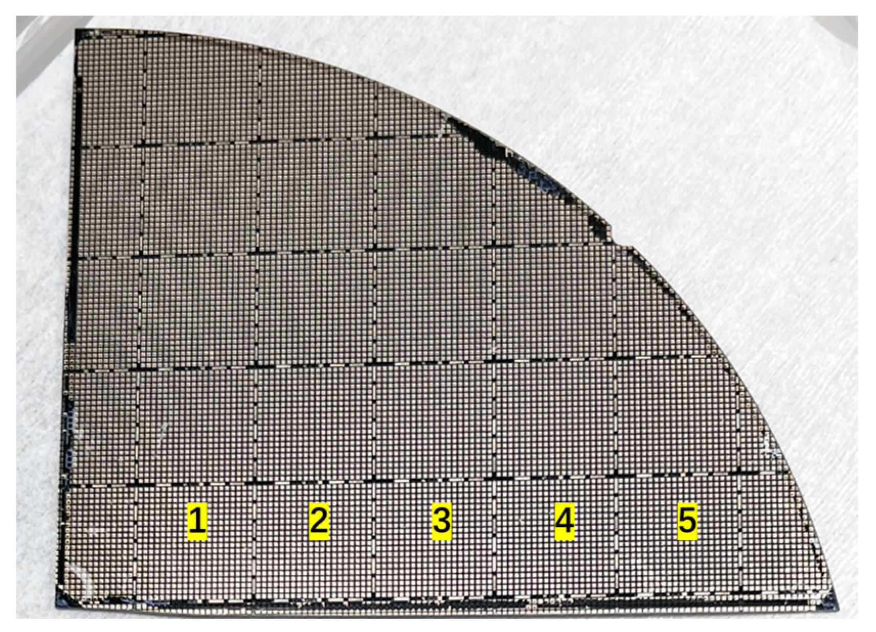
3.2. Impact of Total H2 Flux on the Uniformity of InGaP/GaAs HBTs

Based on the results of the experiment in the previous section, we focused on a specific hydrogen (H2) flux range, from 15,000 sccm to 19,000 sccm, to advance our investigation into the epitaxial growth of InGaP/GaAs HBT structures. This selection was aimed at thoroughly examining the influence of H2 flux on the uniformity of our epitaxial wafers. Throughout these experiments, we adhered to strict growth parameters for the InGaP layer, as outlined in Table 2, while the conditions for the subsequent layers remained constant to guarantee the consistency and reliability of our findings. We successfully developed InGaP/GaAs HBT structures under various H2 flux conditions. Following this, a standard processing protocol was applied to transform these epitaxial wafers into HBT devices. Notably, to directly assess the uniformity of the epitaxial layers, we sidestepped any processing steps, like device encapsulation, which might obscure our observations. The devices were measured in their raw form using a combination of a probing station and a semiconductor parameter analyzer. This direct approach allowed us to precisely evaluate epitaxial wafer uniformity, ensuring that our results were both accurate and reliable, providing a clear picture of the impact of H2 flux on epitaxial layer consistency.
Following the epitaxial growth of InGaP/GaAs HBT structures and device fabrication, we embarked on an in-depth evaluation of the epitaxial wafer’s uniformity. To achieve this, we conducted extensive measurement and analysis across the wafer. We chose five points, ranging from the center to the edge, labelled 1 to 5, each representing a specific device position for measurement. The specific measurement positions are shown in Figure 3. Our examination focused on key electrical performance metrics, including Gummel, IV, and breakdown voltage measurements. The comprehensive assessment of these measurements, comparing results from all selected points, allowed us to gauge the epitaxial wafer’s uniformity accurately. Consistent and stable outcomes across these metrics would indicate a high level of uniformity in our InGaP/GaAs HBT epitaxial wafers. Such uniformity is pivotal for the successful production of high-performance HBT devices, underscoring the effectiveness of our epitaxial growth process in achieving uniform wafer characteristics.

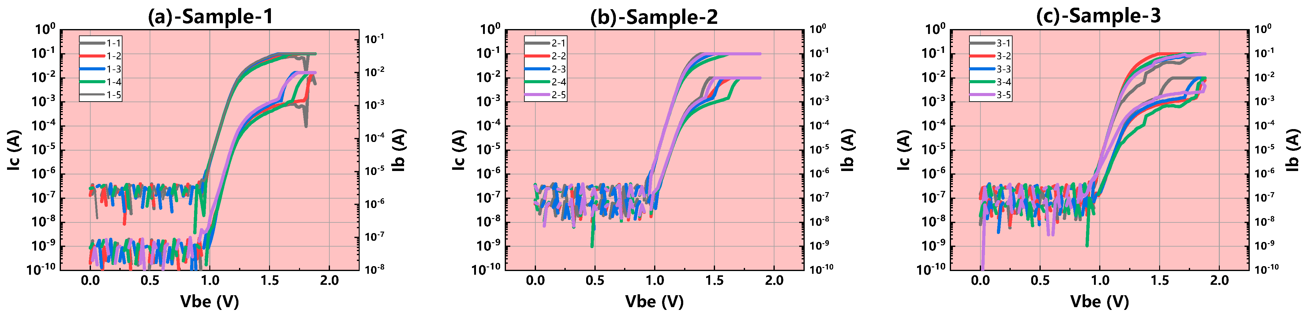
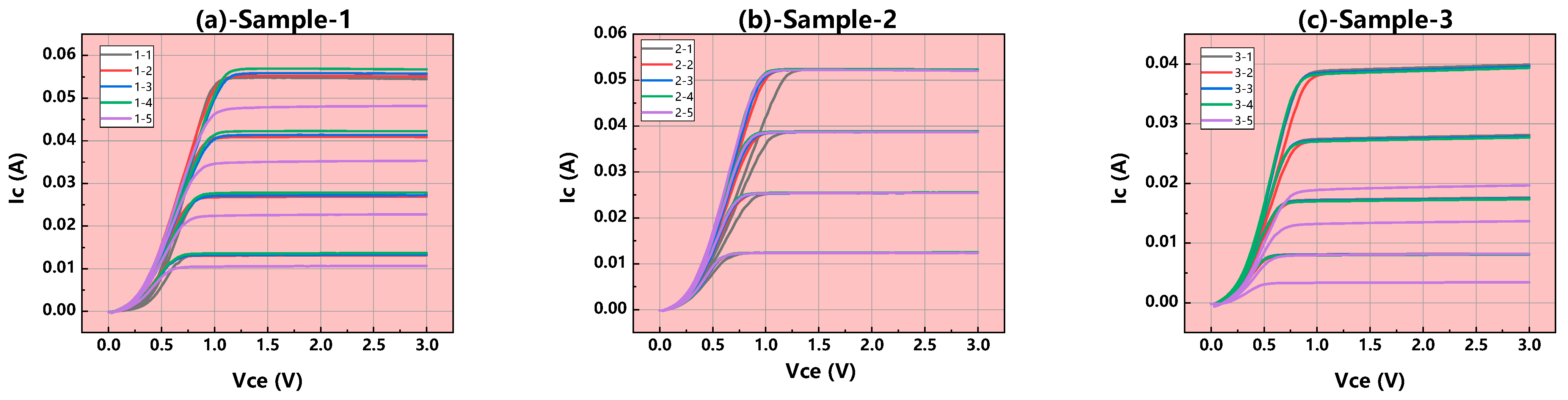
3.2.1. Gummel Curve Measurements

By examining the overlap of Gummel curves at five different points on each sample, we were able to gain insight into the uniformity of the epitaxial wafer. Figure 4 showcases this comparison across three samples, with the degree of curve overlap serving as a visual indicator of uniformity. Sample-2 stands out with the highest degree of overlap, suggesting exemplary uniformity. While Sample-1 also demonstrates commendable overlap, albeit with some variation, it indicates good overall uniformity. Sample-3, however, exhibits significant deviation, particularly in areas of high current density, hinting at potential inconsistencies in the epitaxial wafer’s preparation process that could affect device performance stability. Although this visual assessment offers a preliminary view of uniformity, it lacks a concrete, quantitative benchmark. To refine our understanding of uniformity, we delved into analyzing critical parameters derived from the Gummel curve: the turn-on voltage (Von) and current gain (β). These parameters serve as vital measures of transistor performance, providing a more precise evaluation of the epitaxial wafer’s uniformity.
Through a detailed analysis of the Gummel curves, we derived crucial data on the turn-on voltage and current gain for each of the five measurement points across three samples, as detailed in Table 3. This analysis revealed a remarkable consistency in the turn-on voltage (Von) and current gain (β) values among the measurement points of Sample-2, indicating a uniform performance. Conversely, Sample-1 and Sample-3 displayed more varied data, with Sample-3 showing particularly pronounced disparities among its measurement points, suggesting potential uniformity issues in the epitaxial wafer preparation. To quantify these observations, we calculated the standard deviations of Von and β across the five measurement points for each sample, presented in Table 4. The findings show that Sample-2 exhibits the lowest standard deviation for both Von and β, confirming its superior uniformity and consistency compared to Sample-1 and Sample-3. This quantitative approach underscores the effectiveness of Sample-2’s epitaxial growth process in achieving high uniformity in transistor performance.

3.2.2. IV Output Curve Measurements

We conducted IV output curve assessments at five distinct locations on each of the three samples, facilitating a comparative analysis of these curves within each sample. Figure 5 depicts the outcomes of these evaluations.
Figure 5 presents a comparative analysis of the IV curves for five measurement points across Sample-1, Sample-2, and Sample-3, highlighting the IV curve as a crucial metric for assessing transistor performance through its depiction of device current responses at varying voltages. This comparison reveals a remarkable consistency in Sample-2, where the IV curves of all measurement points nearly overlap completely, underscoring exceptional uniformity. Conversely, Sample-1 and Sample-3 exhibit significantly less overlap, particularly at measurement point 5 (the wafer’s edge), where the IV curves diverge markedly. Such divergence suggests notable inhomogeneities in these samples at the wafer’s edge, potentially attributable to edge effects during epitaxial growth. These effects may alter the epitaxial layer’s thickness, composition, or crystalline quality at the edges, subsequently impacting device performance. Addressing these edge-related variances is crucial for ensuring the stable and reliable performance of HBT devices across the entire wafer.

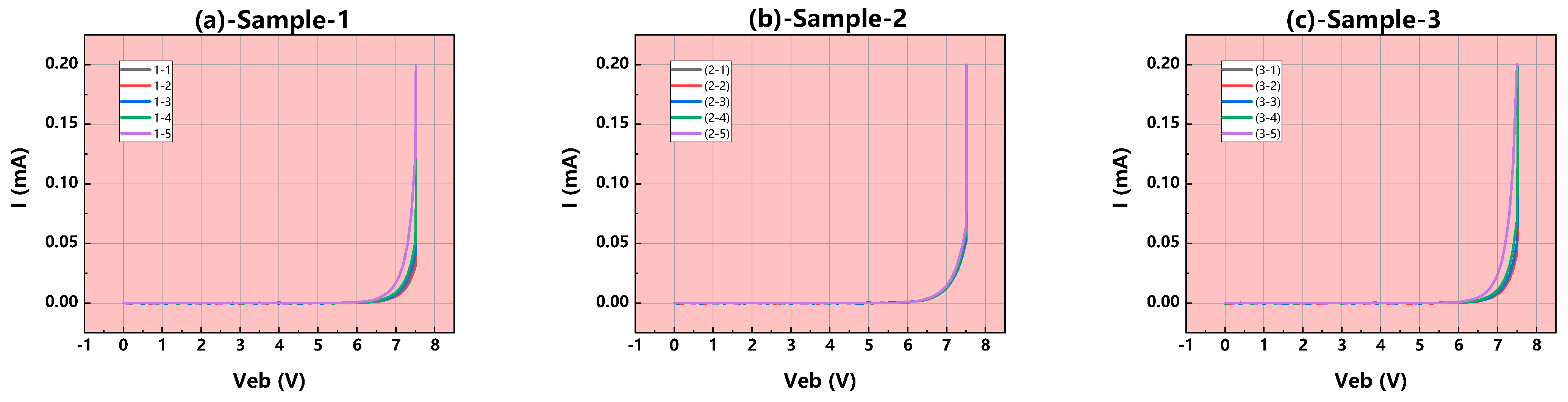
3.2.3. Breakdown Voltage Curve Measurements

Breakdown voltage curves of the emitter-base (EB) junction were analyzed at five specific points across each of the three samples to enable a detailed comparative study of these curves within each sample. The results of this analysis are illustrated in Figure 6.
Figure 6 provides a detailed comparison of the EB junction breakdown voltage curves across five measurement points in Samples 1 to 3. This breakdown voltage is a critical measure of a transistor’s reliability and stability under high-voltage conditions, illustrating the device’s robustness. In Sample-2, the breakdown voltage curves for all measurement points display remarkable alignment, unlike Sample-1 and Sample-3, where variations are noticeable. We further quantified this observation by calculating the standard deviation of the breakdown voltage for each sample’s measurement points, as detailed in Table 5. The findings reveal that Sample-2 has the lowest standard deviation, signifying exceptional uniformity in breakdown voltage. This consistency with the IV and Gummel curve analyses reinforces Sample-2’s superior epitaxial wafer uniformity, highlighting its outstanding performance and reliability as a semiconductor material.
Our comprehensive analysis highlights Sample-2 as exhibiting the highest degree of homogeneity among the measured samples. This conclusion is drawn not only from the comparative study of the breakdown voltage curves and their standard deviation analysis but also from the corroborative evidence provided by the IV and Gummel curve assessments. Furthermore, building upon insights from earlier sections, we deduce that the uniformity of the InGaP layer plays a pivotal role in achieving overall epitaxial wafer uniformity during the HBT growth process. Thus, for the enhancement of HBT device performance, meticulous attention must be given to optimizing the growth conditions and process parameters of the InGaP layer to ensure its uniformity. This strategic focus is crucial for advancing the reliability and performance of HBT devices.

4. Conclusions

In this study, we delved into how the flux of H2 carrier gas influences the uniformity of the InGaP single layer and InGaP/GaAs HBT full-structure epitaxial wafers. Our aim was to uncover the relationship between carrier gas flux and epitaxial layer uniformity, thereby laying a theoretical foundation for optimizing the epitaxial growth process. Our findings reveal that the H2 carrier gas flux critically impacts layer uniformity. At a lower flux, uniformity suffers due to restricted reactant transport velocity, leading to uneven reaction rates and component distribution. Conversely, higher fluxes enhance uniformity by ensuring even reactant distribution across the growth surface. Through comprehensive data analysis, we identified an optimal range for the H2 carrier gas flux that maximizes wafer homogeneity. This discovery is crucial for refining actual epitaxial growth processes. Practically, to stabilize wafer uniformity, increasing the H2 flux is advisable to guarantee uniform reactant transport and distribution. Moreover, we explored the interrelation between the uniformity of the InGaP single layer and the overall structure of InGaP/GaAs HBT epitaxial wafers. The data underscore the significant influence of the uniformity of the InGaP single layer on full-structure wafer uniformity, emphasizing the need for precise adjustments during InGaP/GaAs HBT growth to achieve high-quality epitaxial wafers. In summary, our thorough investigation establishes a significant connection between H2 carrier gas flux and epitaxial layer uniformity. Optimal flux led to enhanced uniformity, a finding that serves as a pivotal guideline for optimizing the epitaxial growth process of InGaP/GaAs HBTs. These insights contribute substantially to the process tuning and industrial fabrication of high-quality uniform InGaP/GaAs HBT epitaxial wafers.

Author Contributions

Data curation, methodology, formal analysis, and writing—original draft preparation, S.Y.; methodology, N.G.; software and visualization, S.Z.; supervision, resources, and investigation, Y.L.; investigation and formal analysis, M.W.; project administration, investigation, and supervision, Y.Z.; conceptualization, supervision, funding acquisition, and writing—review and editing, X.L. All authors have read and agreed to the published version of the manuscript.

Funding

This work was supported by the Key-Area Research and Development Program of Guangdong Province (No. 2021B0101300001) and the Youth Innovation Promotion Association of Chinese Academy of Sciences (Grant No. 2015094).

Data Availability Statement

The data that support the findings of this study are available from the corresponding authors (Y.Z. and X.L.) upon reasonable request.

Conflicts of Interest

The authors declare no conflicts of interest.

References

  1. Yang, Y.-C.; Wan, Z.; Hsu, G.-T.; Chiu, C.-C.; Chen, W.-H.; Feifel, M.; Lackner, D.; Xia, G.; Wu, C.-H. 25 Gb/s NRZ Transmission at 85 °C Using a High-Speed 940 Nm AlGaAs Oxide-Confined VCSEL Grown on a Ge Substrate. Opt. Lett. 2024, 49, 586. [Google Scholar] [CrossRef] [PubMed]
  2. Wan, Z.; Yang, Y.-C.; Chen, W.-H.; Chiu, C.-C.; Zhao, Y.; Feifel, M.; Chrostowski, L.; Lackner, D.; Wu, C.-H.; Xia, G. Monolithically Integrated 940 Nm VCSELs on Bulk Ge Substrates. Opt. Express 2024, 32, 6609. [Google Scholar] [CrossRef] [PubMed]
  3. Xie, S.; Sheikhi, M.; Xu, S.; Alam, M.T.; Zhou, J.; Mawst, L.; Ma, Z.; Gupta, C. P-GaAs/n-Ga2O3 Heterojunction Diode with Breakdown Voltage of ∼800 V. Appl. Phys. Lett. 2024, 124, 073503. [Google Scholar] [CrossRef]
  4. Singh, S.; Samajdar, D.P.; Dutta, K. Systematic Investigation of the Optical Characteristics of GaAs Solar Cells with Antireflection Coatings and Metallic Nanoparticles Using Finite Element Analysis. ACS Appl. Electron. Mater. 2024, 6, 1600–1616. [Google Scholar] [CrossRef]
  5. Liu, Y.; Ma, Y.; Guo, H.; Fu, S.; Liu, Y.; Wei, G.; Liu, Y.; Hao, Y.; Chen, D. The Study of N-Polar GaN/InAlN MOS-HEMT and T-Gate HEMT Biosensors. J. Phys. D Appl. Phys. 2024, 57, 075107. [Google Scholar] [CrossRef]
  6. France, R.M.; McMahon, W.E.; Guthrey, H.L. Critical Thickness of Atomically Ordered III-V Alloys. Appl. Phys. Lett. 2015, 107, 151903. [Google Scholar] [CrossRef]
  7. Steiner, M.A.; Bhusal, L.; Geisz, J.F.; Norman, A.G.; Romero, M.J.; Olavarria, W.J.; Zhang, Y.; Mascarenhas, A. CuPt Ordering in High Bandgap GaxIn1−xP Alloys on Relaxed GaAsP Step Grades. J. Appl. Phys. 2009, 106, 063525. [Google Scholar] [CrossRef]
  8. Li, J.H.; Forrest, R.L.; Moss, S.C.; Zhang, Y.; Mascarenhas, A.; Bai, J. Determination of the Order Parameter of CuPt- B Ordered GaInP2 Films by x-Ray Diffraction. J. Appl. Phys. 2002, 91, 9039–9042. [Google Scholar] [CrossRef]
  9. Schulte, K.L.; Diercks, D.R.; Roberts, D.M.; Dippo, P.C.; Packard, C.E.; Simon, J.; Ptak, A.J. Effect of Hydride Vapor Phase Epitaxy Growth Conditions on the Degree of Atomic Ordering in GaInP. J. Appl. Phys. 2020, 128, 025704. [Google Scholar] [CrossRef]
  10. Attolini, G.; Bocchi, C.; Germini, F.; Pelosi, C.; Parisini, A.; Tarricone, L.; Kùdela, R.; Hasenohrl, S. Effects of Inhomogeneities and Ordering in InGaP/GaAs System Grown by MOVPE. Mater. Chem. Phys. 2000, 66, 246–252. [Google Scholar] [CrossRef]
  11. France, R.M.; McMahon, W.E.; Kang, J.; Steiner, M.A.; Geisz, J.F. In Situ Measurement of CuPt Alloy Ordering Using Strain Anisotropy. J. Appl. Phys. 2014, 115, 053502. [Google Scholar] [CrossRef]
  12. Zakaria, A.; Fetzer, C.M.; Goorsky, M.S. Influence of the Degree of Order of InGaP on Its Hardness Determined Using Nanoindentation. J. Appl. Phys. 2010, 108, 074908. [Google Scholar] [CrossRef]
  13. Ferrini, R.; Guizzetti, G.; Patrini, M.; Parisini, A.; Tarricone, L.; Valenti, B. Optical Functions of InGaP/GaAs Epitaxial Layers from 0.01 to 5.5 eV. Eur. Phys. J. B-Condens. Matter 2002, 27, 449–458. [Google Scholar] [CrossRef]
  14. Longo, M.; Parisini, A.; Tarricone, L.; Toni, L.; Kúdela, R. Photoluminescence Investigation of Superlattice Ordering in Organometallic Vapour Phase Epitaxy Grown InGaP Layers. Mater. Sci. Eng. B 2001, 86, 157–164. [Google Scholar] [CrossRef]
  15. Martín, G.; Coll, C.; López-Conesa, L.; Rebled, J.M.; Barrigón, E.; García, I.; Rey-Stolle, I.; Algora, C.; Cornet, A.; Estradé, S.; et al. Understanding the Anisotropy in the Electrical Conductivity of CuPtB-Type Ordered GaInP Thin Films by Combining In Situ TEM Biasing and First Principles Calculations. ACS Appl. Electron. Mater. 2022, 4, 3478–3485. [Google Scholar] [CrossRef] [PubMed]
  16. Park, G.Y.; Kim, C.W.; Kim, H.J. A Study on Epitaxial Lift-Off in InGaP/GaAs Double-Junction Solar Cells via Au-Au Bonding on Pre-Patterned Area. IEEE Photonics J. 2022, 14, 1–5. [Google Scholar] [CrossRef]
  17. Oh, H.; Shin, J.; Jeon, H.; Woo, Y.Y.; Hwang, K.C.; Lee, K.-Y.; Yang, Y. Broadband InGaP/GaAs HBT Doherty Power Amplifier IC Using Direct Interstage Power Division for Compact 5G NR Handset Module. IEEE Access 2023, 11, 25879–25892. [Google Scholar] [CrossRef]
  18. Liu, Z.; Zhu, H.; Pan, X.; Huang, Y. Burn-in Effect in InGaP/GaAs HBT with Intrinsically or Extrinsically Carbon Doped Base Layer. Phys. Scr. 2023, 98, 065009. [Google Scholar] [CrossRef]
  19. Bauhuis, G.J.; Trinito, V.; Mulder, P.; Schermer, J.J. Characterization of Interface Recombination Velocity in GaAs/InGaP Heterojunction Solar Cells Using Dark Curve Measurements. IEEE J. Photovolt. 2022, 12, 754–759. [Google Scholar] [CrossRef]
  20. Wu, Y.-C.; Tsai, J.-H.; Chiang, T.-K.; Wang, F.-M. Comparative Investigation of InGaP/GaAs/GaAsBi and InGaP/GaAs Heterojunction Bipolar Transistors. Semiconductors 2015, 49, 1361–1364. [Google Scholar] [CrossRef]
  21. Nakamura, T.; Imaizumi, M.; Sato, S.; Ohshima, T.; Akiyama, H.; Okada, Y. Differences in Radiation Damage to Carrier Lifetimes in the Neutral and Depletion Regions of InGaP and GaAs Solar Cells. J. Appl. Phys. 2022, 132, 115701. [Google Scholar] [CrossRef]
  22. Mao, Q.; Huang, L.; Xiang, Z.; Zhu, D.; Meng, J. High-Power Microwave Pulse Induced Failure on InGaP/GaAs Heterojunction Bipolar Transistor. Microelectron. Reliab. 2022, 139, 114848. [Google Scholar] [CrossRef]
  23. Hashem, I.E.; Zachary Carlin, C.; Hagar, B.G.; Colter, P.C.; Bedair, S.M. InGaP-Based Quantum Well Solar Cells: Growth, Structural Design, and Photovoltaic Properties. J. Appl. Phys. 2016, 119, 095706. [Google Scholar] [CrossRef]
  24. Asami, M.; Watanabe, K.; Nakano, Y.; Sugiyama, M. Smooth Surface Morphology and Long Carrier Lifetime of InGaP Realized by Low-Temperature-Grown Cover Layer. Phys. Status Solidi B 2022, 259, 2100305. [Google Scholar] [CrossRef]
  25. Huang, C.H.; Tan, S.W.; Lo, H.; Lo, C.; Lour, W.S. Temperature Dependence of Sensing Properties of Hydrogen-Sensitive Extended-Base Heterojunction Bipolar Transistors. Int. J. Hydrogen Energy 2022, 47, 39276–39287. [Google Scholar] [CrossRef]
  26. Zhu, L.; Wang, Y.; Pan, X.; Akiyama, H. Theoretical Modeling and Ultra-Thin Design for Multi-Junction Solar Cells with a Light-Trapping Front Surface and Its Application to InGaP/GaAs/InGaAs 3-Junction. Opt. Express 2022, 30, 35202. [Google Scholar] [CrossRef] [PubMed]
  27. Orzali, T.; Vert, A.; O’Brian, B.; Herman, J.L.; Vivekanand, S.; Papa Rao, S.S.; Oktyabrsky, S.R. Epitaxial Growth of GaSb and InAs Fins on 300 Mm Si (001) by Aspect Ratio Trapping. J. Appl. Phys. 2016, 120, 085308. [Google Scholar] [CrossRef]
  28. Orzali, T.; Vert, A.; Kim, T.-W.; Hung, P.Y.; Herman, J.L.; Vivekanand, S.; Huang, G.; Kelman, M.; Karim, Z.; Hill, R.J.W.; et al. Growth and Characterization of an In0.53Ga0.47As-Based Metal-Oxide-Semiconductor Capacitor (MOSCAP) Structure on 300mm on-Axis Si (001) Wafers by MOCVD. J. Cryst. Growth 2015, 427, 72–79. [Google Scholar] [CrossRef]
  29. Heinecke, H.; Veuhoff, E.; Pütz, N.; Heyen, M.; Balk, P. Kinetics of GaAs Growth by Low Pressure MO-CVD. JEM 1984, 13, 815–830. [Google Scholar] [CrossRef]
  30. Qin, B.; Ma, H.; Hossain, M.; Zhong, M.; Xia, Q.; Li, B.; Duan, X. Substrates in the Synthesis of Two-Dimensional Materials via Chemical Vapor Deposition. Chem. Mater. 2020, 32, 10321–10347. [Google Scholar] [CrossRef]
  31. Tsang, W.T. The Growth of GaAs, AIGaAs, InP and InGaAs by Chemical Beam Epitaxy Using Group III and V Alkyls. J. Electron. Mater. 1986, 15, 235–245. [Google Scholar] [CrossRef]
  32. Yu, D.; Shen, S.; Li, H.; Shen, W. Design Optimization of Gas Distribution System for Large-Scale Capacity GaAs-MOCVD. Cryst. Res. Technol. 2023, 58, 2300186. [Google Scholar] [CrossRef]
  33. Sodabanlu, H.; Ubukata, A.; Watanabe, K.; Sugaya, T.; Nakano, Y.; Sugiyama, M. High-Speed MOVPE Growth of InGaP Solar Cells. IEEE J. Photovolt. 2020, 10, 480–486. [Google Scholar] [CrossRef]
  34. Hino, M.; Asami, M.; Watanabe, K.; Nakano, Y.; Sugiyama, M. InGaP Solar Cell with InGaP Multiple Quantum Wells Grown under Optimized V/III Ratio. Phys. Status Solidi A 2023, 220, 2300660. [Google Scholar] [CrossRef]
  35. Armani, N.; Abagnale, G.; Trespidi, F.; Cornelli, M.; Timò, G.; Malvisi, E.; Farina, F.; Carbi, G.; Rossi, F.; Fabbri, F.; et al. Low Growth Temperature MOCVD InGaP for Multi-Junction Solar Cells. Energy Procedia 2015, 84, 34–40. [Google Scholar] [CrossRef]
  36. Chuang, Y.-C.; Chen, C.-T. Mathematical Modeling and Optimal Design of an MOCVD Reactor for GaAs Film Growth. J. Taiwan Inst. Chem. Eng. 2014, 45, 254–267. [Google Scholar] [CrossRef]
  37. Féron, O.; Sugiyama, M.; Asawamethapant, W.; Futakuchi, N.; Feurprier, Y.; Nakano, Y.; Shimogaki, Y. MOCVD of InGaAsP, InGaAs and InGaP over InP and GaAs Substrates: Distribution of Composition and Growth Rate in a Horizontal Reactor. Appl. Surf. Sci. 2000, 159–160, 318–327. [Google Scholar] [CrossRef]
  38. Lin, Y.S.; Huang, D.H.; Chen, Y.W.; Huang, J.C.; Hsu, W.C. δ-Doped InGaP/GaAs Heterostructure-Emitter Bipolar Transistor Grown by Metalorganic Chemical Vapor Deposition. Thin Solid Film. 2007, 515, 3978–3981. [Google Scholar] [CrossRef]
Figure 1. The sheet resistance measurements, corresponding to varying total H2 fluxes, are shown sequentially for the rates of 15,000 sccm, 17,000 sccm, 19,000 sccm, and 21,000 sccm from (a) to (d).
Electronics 13 02109 g001
Figure 2. (a) Influence of total H2 flux on epitaxial growth rate. (b) Impact of total H2 flux on sheet resistance and its uniformity.
Electronics 13 02109 g002
Figure 3. Photograph of the InGaP/GaAs HBT Chip; the yellow regions (1–5) indicate the five measurement positions.
Electronics 13 02109 g003
Figure 4. Comparative analysis of Gummel curves at five measurement points for the samples.
Electronics 13 02109 g004
Figure 5. IV curve comparison for 5 measurement points for the samples.
Electronics 13 02109 g005
Figure 6. Comparison of EB junction breakdown voltage curves at 5 measurement points for the samples.
Electronics 13 02109 g006
Table 1. The impact of total H2 flux on the properties of epitaxial layers. The H2 flux, growth temperature, and V/III ratio for each sample are shown.
Sample No.H2 FluxGrowth TemperatureV/III
Sample-a15,000 sccm650 °C80
Sample-b17,000 sccm
Sample-c19,000 sccm
Sample-d21,000 sccm
Table 2. Growth conditions for the InGaP layer across all samples within the complete HBT epitaxial structure.
Sample No.H2 FluxGrowth TemperatureV/III
Sample-119,000 sccm650 °C80
Sample-217,000 sccm
Sample-315,000 sccm
Table 3. Current gain and opening voltage analysis at five measurement points for Sample-1, Sample-2, and Sample-3.
Measurement ContentSample No.12345
β Sample-159.960.661.762.550.6
Sample-258.357.957.757.657.1
Sample-354.955.554.452.653.1
V on (V)Sample-12.191.842.082.081.70
Sample-21.701.821.711.701.82
Sample-31.961.821.831.821.78
Table 4. Analysis of the standard deviations of current gain and opening voltage across five measurement points for Sample-1, Sample-2, and Sample-3.
Sample No.Standard Deviation of V on   ( V ) Standard Deviation of β
Sample-10.203594.83070
Sample-20.062440.46892
Sample-30.073101.23464
Table 5. The breakdown voltage of the EB junction corresponding to the 5 measurement points for Sample-1, Sample-2, and Sample-3.
Measurement Content12345Standard Deviation of BV eb  (V)
BV eb   ( V ) 5.85.85.75.75.50.12249
5.85.85.75.75.70.05477
5.75.75.75.65.40.13039
Disclaimer/Publisher’s Note: The statements, opinions and data contained in all publications are solely those of the individual author(s) and contributor(s) and not of MDPI and/or the editor(s). MDPI and/or the editor(s) disclaim responsibility for any injury to people or property resulting from any ideas, methods, instructions or products referred to in the content.

