Abstract
This article deals with power supply linear and switching regulators commonly used in various applications for stabilizing an output voltage and ensuring a necessary power input to the load. It describes their basic parameters, performances, advantages, and disadvantages according to their topologies. We design a measurement chain for efficiency evaluation based on power monitors INA219 connected to an embedded system, Arduino UNO. Measurements were focused on evaluation linear regulators MA7805, LM317, switching regulators SZBK07, LM2575, SCW05B-05, and XH-M401. The resulting efficiency of linear and switching regulators was analyzed and errors in the measurement chain were evaluated. The second contribution is an innovative way of carrying out regulator noise estimation using a fast Allan variance method, focused on white noise and flicker noise (bias instability). The main contribution is employing a fast Allan variance method algorithm that dramatically decreases computation time by up to 11 s for 72 million measured (or generated) samples. It enables the analysis of large data sets of various physical quantities (for example, regulator output voltages).
1. Introduction
Power supply (units) are devices producing nominal voltage and currents for various systems and devices in simple or difficult applications. They can be sorted according to type of regulation principle, according to input/output voltage/current values (AC/DC, DC/DC, DC/AC), or according to their used physical principles (chemical, electric induction, electrostatic, photovoltaic, thermoelectric) as in [1,2,3,4,5].
Power supplies can be sorted according to regulation principle [4,5] into the continuous (linear power supply) or switching power supply. Power supplies that can use energy from a public distribution grid are very often referred to as grid power supplies (Figure 1).
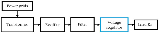
Figure 1.
Grid power supply.
Grid power supplies connected to public distribution grids usually consist of a transformer, rectifiers, filters, and voltage regulators connected to a load. The voltage regulator is used for stabilizing output voltage values () when input voltage or load is changing.
2. Literature Review
The advantages and disadvantages of linear and switching power supply topologies are summarized in Table 1, where the efficiency of switching power supply reaches higher values in comparison with linear power supply.

Table 1.
Comparison of four power supply typologies. Adapted from [5].
From the comparison in Table 1 and according to Figure 1 [5], the big influence onefficiency and noise properties is the power supply topology and choice of voltage regulator.
Because linear regulators are step-down regulators, the required output voltage, , is smaller than the input source voltage, . Shunt regulators and series-pass regulators are the two varieties of linear regulators [4,5].
A voltage regulator that is connected in parallel to the load is called a shunt regulator. A higher voltage source is linked to an unregulated current source, and given a changing input voltage and load current; a shunt regulator pulls output current to maintain a constant voltage across the load. This is frequently seen in Zener diode regulators.
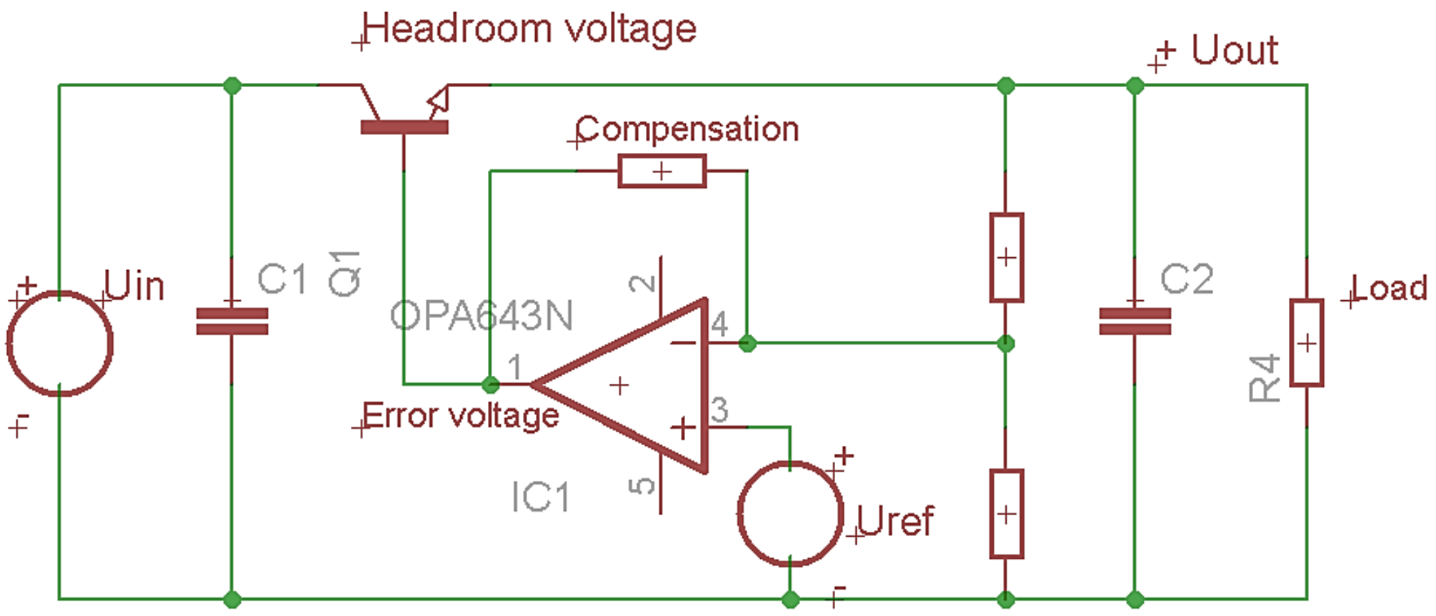
Compared to the shunt regulator, the series-pass linear regulator (Figure 2) is more effective and widely utilized. An active semiconductor (NPN transistor), coupled between the input source and the load, serves as the series-pass element in a series-pass linear regulator [4,5].
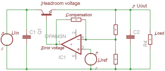
Figure 2.
The series-pass regulator.
The linear mode of operation for the series-pass unit indicates that it is not intended to work in a fully on or off mode but rather to operate in a state of “partial on”. The pass unit’s necessary level of conductivity is determined by the negative feedback loop [4,5]. In this manner, the output voltage value Uout is sustained.
A voltage error amplifier, or high-gain operational amplifier (OpAmp), is the main element in the negative feedback loop. Its goal is to continually compare the output voltage with a very reliable voltage reference.
A time invariant refence voltage is typically less than the output voltage and is connected to the OpAmp’s noninverting input. To reach the voltage reference level, the output voltage value is divided down. The operational amplifier’s inverting input is fed with this divided output voltage. The output voltage divider’s center node is therefore the same as the reference voltage at the rated output voltage [4,5].
The voltage generated by the error amplifier’s gain is a representation of the significantly amplified difference between the output voltage (error voltage ) and the reference voltage . By directly regulating the pass unit’s conductivity, the error voltage keeps the rated output voltage constant.
The output voltage will decrease with an increase in the load. As a result, the output of the amplifier will rise, giving the load greater current. A decrease in the load will also cause the output voltage to rise, which will cause the error amplifier to react by reducing the pass unit current to the load [4,5].
The real voltage drop that occurs during operation between the input and output voltages is known as the dropout voltage. This voltage drop loses more than 95% of the total power lost within the linear regulator. Based on the following, this headroom loss is calculated as follows:
The PWM switching power supply operates the power transistors in both the saturated and cutoff states, in contrast to linear regulators that only operate the power transistor in the linear mode [5]. Under these conditions, the power transistor’s volt-ampere product is consistently maintained at a low level (saturated, low voltage/high current; and cutoff, high voltage/no current).
By “chopping” the direct current (dc) input voltage into pulses whose duty cycle is regulated by a switching regulator controller and whose amplitude is equal to the input voltage, the PWM switching power supply operates more efficiently. A transformer can be used to step up or down the amplitude once the input voltage has been transformed into an ac rectangular waveform. A transformer’s secondary can be added to generate additional output voltages. In the end, the dc output voltages are obtained by filtering these ac waveforms.
The controller functions a lot like a linear-style controller, with its primary goal being to maintain a controlled output voltage. In other words, the arrangement of the error amplifier, voltage reference, and functional blocks is the same as that of the linear regulators. The distinction lies in the fact that the error voltage, obtained from the error amplifier, is then sent into a voltage-to-pulse-width converter stage before the power switches are activated [5].
The forward-mode converter and the boost-mode converter are the two main operational types of switching power supply [1,2,3,4,5]. Switching power supply topologies based on their operational principle (structure) are mentioned in Table 2, where their power ranges, typical efficiency, and other characteristics can be seen [5].
Table 2.
Summarization of the PWM switching regulator topologies. Adapted from [5].
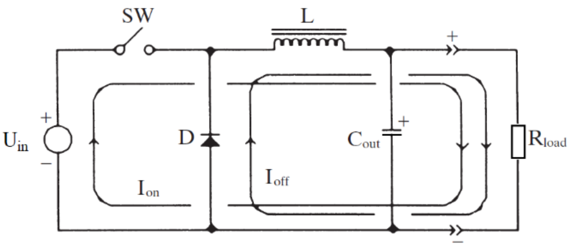
A wide family of switching power supply transformers includes forward-mode regulators. An L-C filter placed directly after the power switch or the output rectifier on a transformer’s secondary can be used to identify them. Figure 3 shows a basic version of the forward-mode regulator.
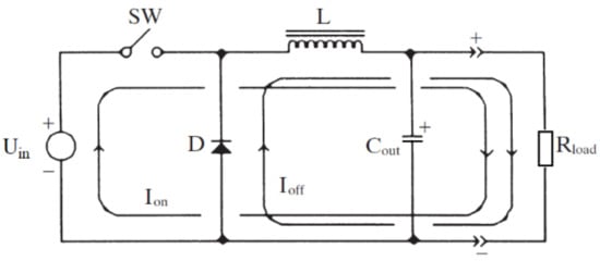
Figure 3.
A basic forward-mode converter (buck converter) [5].
This topology is called the buck regulator. Between the driver’s power pulses, the L-C filter stores energy. The chopped input voltage is the input to the L-C filter, also known as the choke input filter. This duty-cycle δ modulated input voltage waveform is volt-time averaged by the L-C filter. An approximation of the L-C filtering function is as follows:
where is a switch-on time of the switch SW, and is a period of buck converter.
The controller maintains the output voltage by adjusting the duty cycle δ, which is specified differently based on the switching power supply topology that is being used. Because its output must be lower than the input voltage, the buck converter is also referred to as a step-down converter [5].
3. Methodology and Analysis
Voltage regulators are parts of power supplies in various types of power supplies, which are responsible for the stabilization of load voltage values at user-defined intervals. They define basic power supply parameters: input/output current and voltage ranges (), constant on changing output loads (), efficiency , line regulation, load regulation, ripple, noise, and others. Protection and safety are important functionalities of regulators too.
3.1. Main Characteristics of Voltage Regulators
The ability of a power supply to maintain a constant output voltage while allowing the output current (also known as ) drawn from the power supply to remain constant is known as line regulation [4,5]. Line regulation is defined according to the following equations:
Line regulation is expressed in regulator device datasheets as a percentage change in an output relative to a change in an input per volt of the output, as in [5,6,7,8,9,10,11].
The ability of a power supply to maintain a steady voltage (or current) level on its output channel in the face of changes in the supply’s load, such as a variance in the resistance across the supply output, is known as load regulation. This is defined by:
where is load voltage when load current is minimal, and is load voltage when load current is maximal.
An efficiency is a regulator’s ability to provide necessary values of output voltage and current (power ) for load. A power is derived from the input power at the input of a regulator. The efficiency is generally defined as:
where output power for switching power supplies can be estimated according to [5]:
In producers’ datasheets (typical) efficiency represents a value or values when the maximum current flows through the regulator that gives a maximal efficiency value (see [10]).
A ripple is a parasitic AC component of regulator output DC voltage. This is measured in volts (peak-to-peak), and its frequency and level should be acceptable to load circuits. For example, the LM2575 switching regulator has a sawtooth-ripple voltage at the switching frequency—typically about 1% of the output level voltage, as can be seen in [10].
Unintentional generation of conducted or radiated energy is represented by electromagnetic interference (EMI), or radiofrequency interference (RFI). For all switching-mode power supplies, EMI is described. A large interference spectrum is produced by the quick rectangular switching action needed for good efficiency, which can be a serious issue.
There are two forms of EMI propagation: electromagnetic radiated components of and fields and conducted interference on supply and interconnecting lines.
Each power supply or its regulator can produce unwanted noise and this noise is a part of the power supply output voltage brought to load.
3.2. Estimation of Power Supply Regulator Noise using the Fast Allan Variance Method
Estimation of noises using simple sensors or more complex electronic systems can be realized according to the following methods: Allan variance (AVAR), power spectral density (PSD), and autocorrelation function (ACF). For computation, the PSD employs a frequency-averaging technique and the AVAR method uses a time-averaging technique. AVAR is the method widely used thanks to its simplicity. The AVAR method’s benefits are its relatively simple computation principle and visualization (evaluation ability) of sensor noises [12,13].
The AVAR method assesses the noise coefficients and characteristic noises of inertial sensors, such as acceleration ramp AccR (Rate Ramp RR), velocity random walk VRW (Angle Random Walk ARW), quantization noise, sinusoidal noises, exponentially correlated (Markov) noise, bias instability BI, and acceleration random walk AccRW (Rate Random Walk RRW) [12,13,14,15].
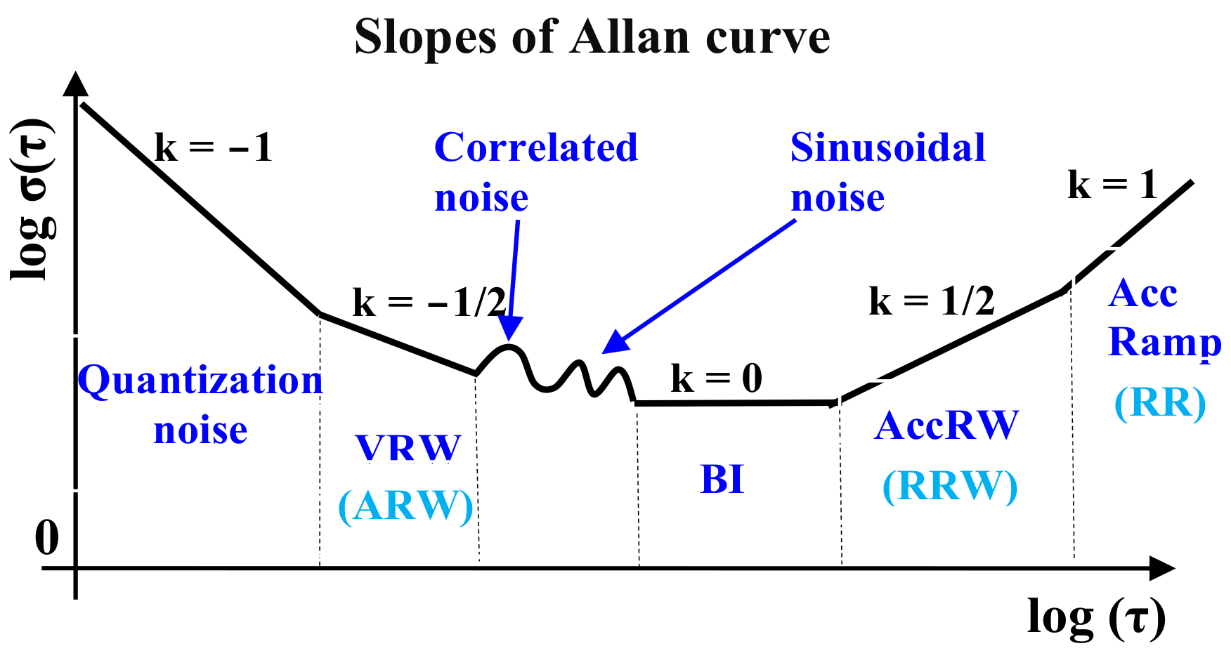
The calculation of the root mean square random drift error as a function of average time is the foundation of the AVAR method. According to Figure 4, the square root of the Allan deviation (ADEV), or log–log plot of AVAR, is utilized for the practical noise determination.

Figure 4.
Example of Allan variance curve.
AVAR is computed according to the following equation [12]:
where is the number of cluster samples (). Average values of the clusters are computed as follows:
where . The cluster size m is defined by the number of averaged samples N where . For nonoverlapped cluster sampling methods, step equals [12].
The percentage error in the AVAR accuracy is determined by the following equation:
From the value, confidence intervals for (68%) are computed according to:
The nonoverlapped method was selected for AVAR computation due to its computational efficiency and ease of use. As defined by (9) and (10), the nonoverlapped method’s relatively higher error level is a drawback.
Thanks to the AVAR method and from the Allan curve, different types of inertial sensors’ stochastic errors could be estimated, where the Allan curve region with a slope of is important for white noise amplitude estimation and the minimal ADEV value is important for flicker noise estimation. Both of those noises are characteristic noises which are important for producers and designers of electronic devices.
Angle random walk ARW (or velocity—VRW) with white frequency modulation noise, is a high frequency noise that has a correlation time that is less than the sample time. At the sensor output, ARW is represented as white noise [14,15].
A common source of white noise for (inertial) sensors and power supplies is the chaotic movement of charge carriers in conductive leads and semiconductor devices. ARW, which represents a white noise, is expressed according to
where is a proportional value which is related to ARW and is the white noise coefficient. According to [12,16], it is expressed as
The Allan curve or the line with a slope of −1/2 at can be used to determine the value of the coefficient , as shown in Figure 4.
Low-frequency noise represents bias instability, also known as flicker frequency modulation, or FFM. Low-frequency flicker noise arising from electronic parts and sensor devices can be a cause of bias instability. According to AVAR, bias instability can be expressed as follows:
where , is the cosine integral function, is cutoff frequency, and is a bias instability coefficient. As seen in Figure 4, the bias instability level is estimated from a flat region (line with slope 0). Coefficient is computed from the ADEV minimal value from Figure 4, and it is divided by the value [12].
In general, white noise and flicker noise are characteristic noises of inertial sensors because of their great influence on inertial parameters (acceleration, speed, angular rate, angles) determinations. Other noise types are quantization noise, sinusoidal noise and Markov correlated noise. They may or may not be significant (distinguishable) in noise analysis with respect to the level of characteristic types of noise when noise analysis methods are used.
The long correlation noise types in Figure 4 (regions AccRW/RRW, AccRamp/RR) are important for precise inertial sensors category. For a power supply, they can describe long-lasting slow fluctuations of that can be determined by changing inner and external conditions (temperature) and so on.
The limit case of exponentially correlated noise with a very long correlation time is rate (or acceleration) random walk RRW (AccRW) (random walk frequency modulation RWFM) [12,17]. In both the frequency domain (PSD) and the time domain (), RRW is expressed as
where is associated PSD, K is the rate (or acceleration) random walk coefficient, and is the proportional part of AVAR associated with RRW (or AccRW). In Figure 4, the region with a slope of +1/2 can be used to evaluate RRW. The line with a slope of +1/2 at = 3 on the Allan curve is used to estimate the value of the coefficient .
4. Measurement Results
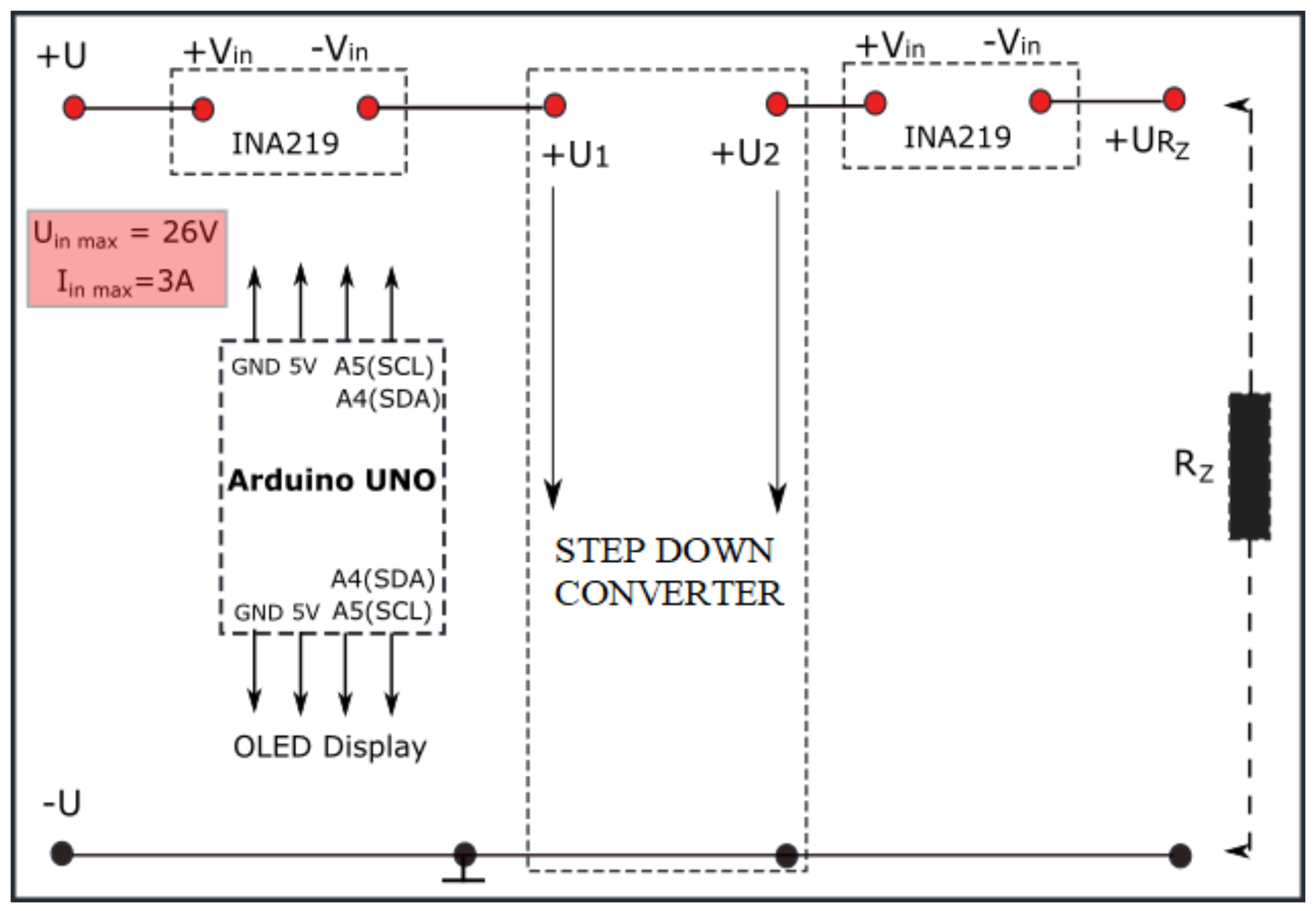
The measurement site in Figure 5 consists of laboratory equipment for efficiency measurement based on INA219 integrated circuits, a QL355TP power supply, data acquisition system NI USB6363, and a PC connected via a USB port to the host microcontroller on the Arduino UNO board. Linear voltage regulators MA7805CV, LM317 and switching DC-DC regulators SCW05B-05, LM2575, XH-M401, resistive load and 300 W buck converters were chosen for the experiments.
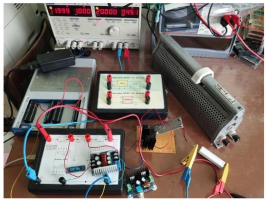
Figure 5.
The measurement site.
The equipment used for efficiency measurement consists of two INA219 development boards, an Arduino UNO evaluation board and an OLED display.
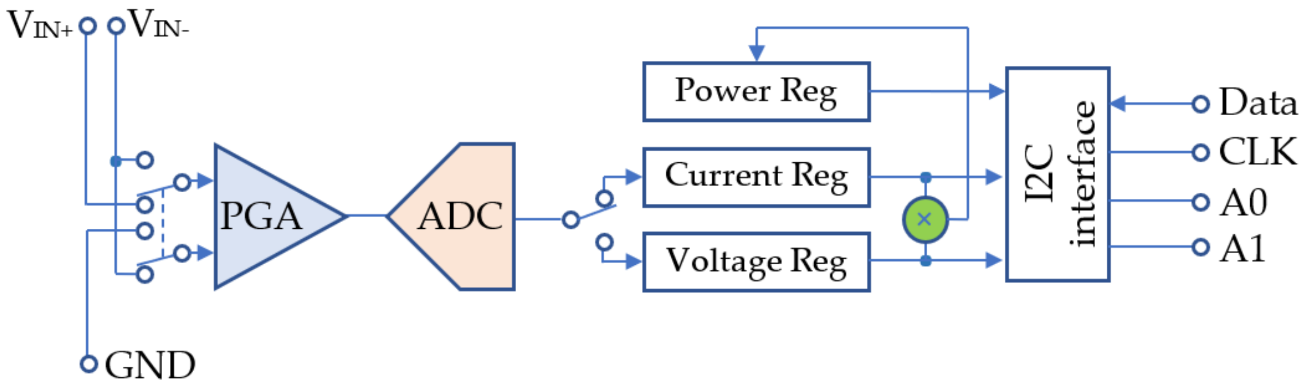
The INA219 development board, shown in Figure 6, is an I2C-enabled hide-side power and current shunt monitor [18]. The INA219 monitors both shunt drop and supply voltage, with programmable conversion times and filtering. An additional multiplying register calculates power in watts. Voltages across shunts on buses that range from 0 V to 26 V are sensed by the INA219 device. The INA219 ADC has a 12-bit basic resolution.

Figure 6.
INA219 power monitor structure.
The voltage across the 0.1 Ohm, 1% sense resistor is measured by a precision amplifier connected between and . The amplifier can measure up to ±3.2 A because its maximum input difference is ±320 mV. The resolution at ±3.2 A range with the internal 12-bit ADC is 0.8 mA. The maximum current is ±400 mA and the resolution is 0.1 mA when the internal gain is set to the lowest possible value.
The principle of current measurement is based on Ohm’s law and a current is computed according to [18]:
where the first Least Significant Bit (1LSB) shunt voltage represents the value 10 µV, and is a voltage on a shunt resistor . INA219 uses a programmable amplifier because the measured shunt voltage is a low value.
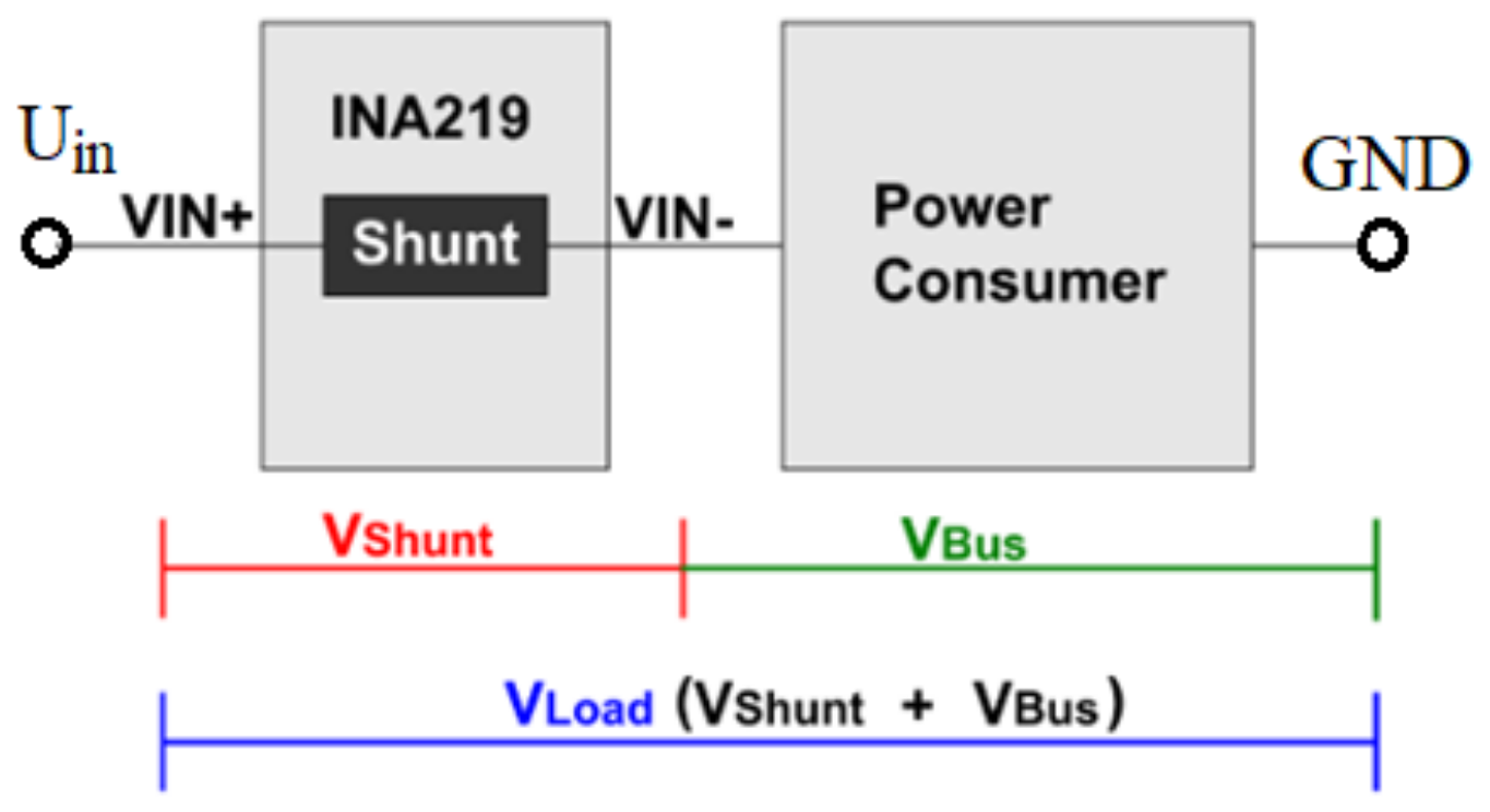
Evaluation board INA219 measures bus voltage between pin and GND as in Figure 7. From bus voltage and current value , power on load is computed according to
where 1LSB of bus voltage is a value of 4 mV. This is a high-side connection because INA219 is connected to the power supply behind the load [18].
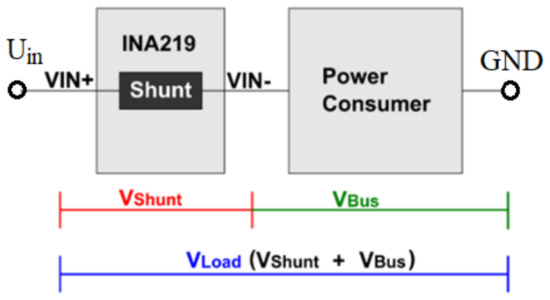
Figure 7.
INA219 measurements.
The main task of the two INA219 measurements in Figure 8 is to measure the input/output voltages and input/output currents of the chosen linear and switching regulators.
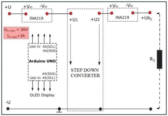
Figure 8.
An efficiency measurement.
Communication with two INA219 boards was realized by using a I2C interface where I2C addresses were set at 0 × 40 and 0 × 41 according to [18,19]. A measured value of current, voltage and power were sent to the Arduino UNO development board. In the Arduino development board, efficiency values according to (5) and (6) were computed. The efficiency, input/output voltages and currents are shown on the OLED display.
4.1. Efficiency Evaluation of Regulator Samples
For the experiments, we chose two linear regulators MA7805, LM317 and four switching regulators SZBK07, LM2575, SCW05B-05, and XH-M401.
Linear regulator MA7805 is a fixed regulator [6], and it is designed to provide a constant voltage of 5 V and a current up to 1.5 A. Producers declare its output noise voltage to be 10 µV/.
Linear regulator LM317 is an adjustable voltage regulator that provides a voltage of 1.2 up to 40 V and a current of up to 1.5 A. Producers do not specify efficiency values for this linear regulator. The producer (Texas instruments) declares an RMS noise value of only 0.003% of (10 Hz ≤ f ≤ 10 kHz) [7].
LM2575 is a simple step-down switching regulator [10] designed for a wide voltage output range from 1.23 to 37 V and for input voltage values from 4.75 to 40 V. The regulator is designed for output current values up to 1 A and it uses a fixed frequency internal oscillator (52 kHz). Producers generally specify an efficiency of 88%; however, it is defined only for specific conditions in the datasheets: 12 V, 5 V, 1 A up to 77%. An output ripple depends on capacity and it varies from 20 mV up to 150 mV. The producer in [10] does not define an output noise for the regulator.
XH-M401 is a power supply module board based on a DC-DC buck converter XL4016. It operates within an input voltage range from 4 up to 40 V and has an adjustable output voltage in the range from 1.25 up to 36 V. The module board XH-M401 provides a maximum of 8 A and 200 W. The producer defines its efficiency as being up to 94% at a switching frequency of 180 kHz. The output ripple and noise parameters are not defined. The DC-DC converter XL4016 producer (XLSEMI) defines the efficiency as being up to 96%; however, it depends on , and as in [11].
The SZBK07 DC-DC adjustable buck converter module is a constant current voltage regulator used for power supplies of LED drivers or in photovoltaic power supplies. It operates at a switching frequency of 180 kHz.
It uses a DC-DC step down buck converter LM5116 with NCE8580 MOSFET transistors and it is intended for an input voltage range from 6 V up to 40 V. It provides an output voltage from 1.2 V to 36 V for load currents up to 20 A and its maximal power is 300 W. The efficiency of SZBK07 can be up to 96%, measured at 20 A, converting 24 V to 12 V. An output ripple can be up to 50 mV [8].
Based on measurements realized by IN219 modules, an efficiency of above the mentioned linear and switching regulators was computed according to Equations (5) and (6). The efficiency evaluation was performed for input voltage 20 V and 10 V and for 5 V at the output of the regulators. A resistive load was used for adjusting the output current in the range from 0 to 400 mA.
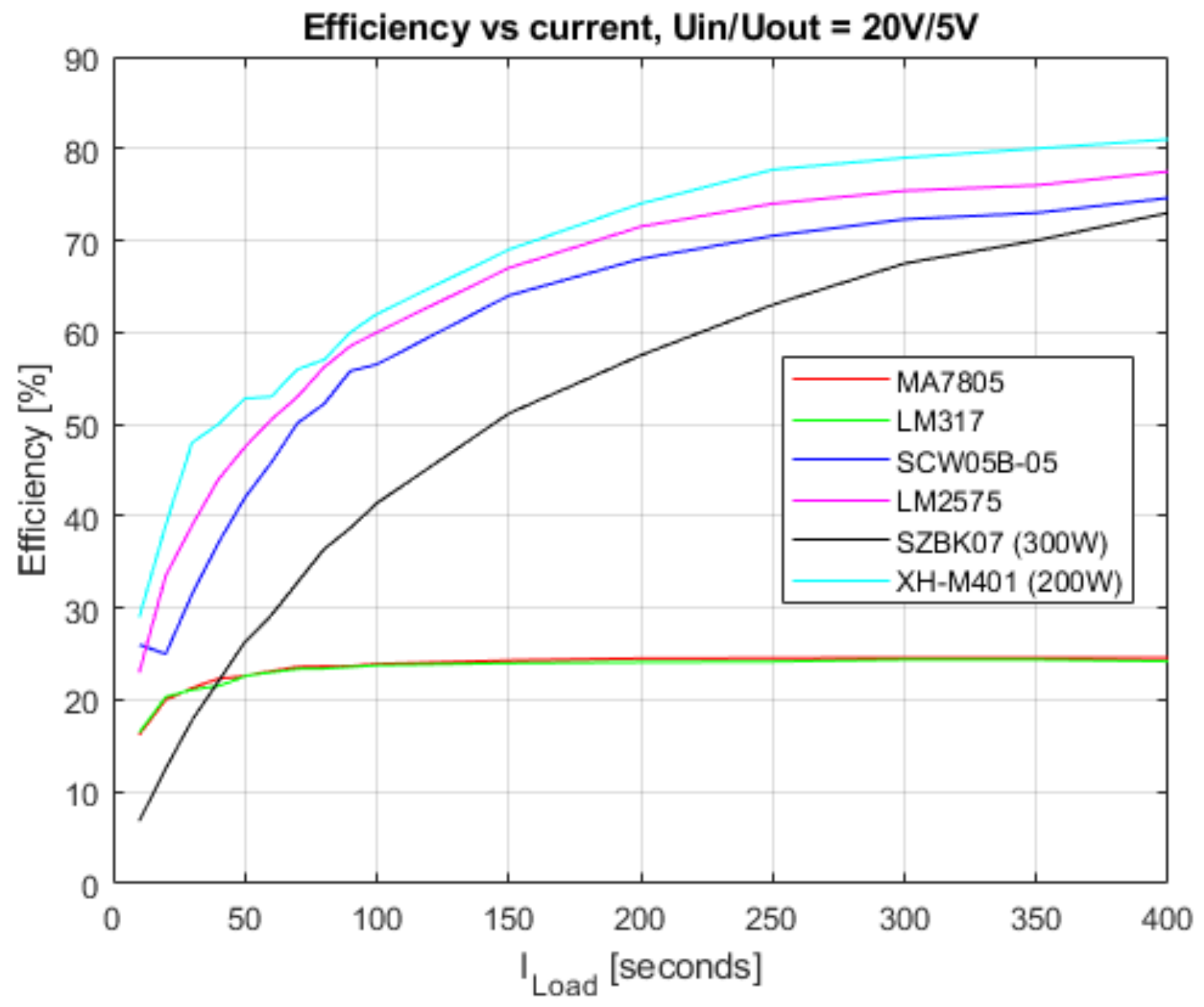
As can be seen in Figure 9, for 20 V and 5 V, the efficiency of both linear regulators reaches the lowest values. Their efficiency starts from 16% for load currents of tens mA and for higher load currents it reaches up to 24.6%.
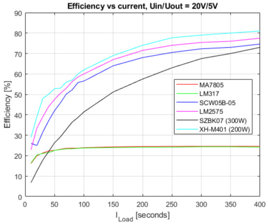
Figure 9.
Efficiency of regulators at 20 V, 5 V.
The efficiency of switching (buck) regulators starts at relatively low values, in comparison with the declared (typical or maximal) efficiency in the producers’ datasheets [6,7,8,9,10,11]. According to Figure 9, the lowest efficiency can be seen in the low load current region, where switching regulators SZBK07, LM2575, SCW05B-05, and XH-M401 reach efficiencies of 6.8%, 23%, 26%, and 29%, respectively. The efficiency of these regulators increases rapidly at high load currents and reaches maximal values of 73%, 75%, 78%, and 81%, respectively.
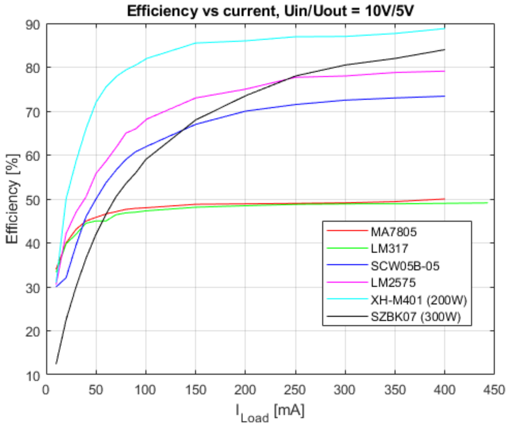
As can be seen in Figure 10, for 10 V and 5 V, the efficiency of linear regulators does not reach the lowest values in comparison with the SCW05B-05 and SZBK07 switching regulators. The efficiency values of the linear regulators starts at 33–34% for load currents in tens mA, and by increasing load current, these values reach approximately 50%.

Figure 10.
Efficiency of regulators at 10 V, 5 V.
From Figure 10, we can see the efficiency of switching (buck) regulators starts at relative low values, in comparison with their declared (typical or maximal) efficiency in the producers’ datasheets [6,7,8,9,10,11].
The lowest efficiency values are found in the low load current region, where switching regulators SZBK07, LM2575, SCW05B-05, and XH-M401 reach the efficiency of 12.4%, 30.5%, 30%, and 31%, respectively. The switching regulators’ efficiency dramatically increases with increasing load current, and it reaches 84%, 73.4%, 79.1%, and 88.8% respectively.
According to Figure 9 and Figure 10, the switching regulator analysis shows their efficiencies are higher (compared to linear regulators) in the region of higher load currents. In the low load current region, this statement is not valid. However, power losses in this region are not as significant as in the region of higher load current values.
Analyzed efficiency depends on measurement errors produced by INA219 and its resolution. INA219 is a universal circuit that can use different values of shunt resistors. In the measurement site, a 0.1 Ohm (1%) shunt resistor was used. INA219 has a resolution of 0.8 mA in the range of ±3.2 A (12 bit resolution, conversion time 586 μs) and bus voltage was measured using a 4 mV resolution [18].
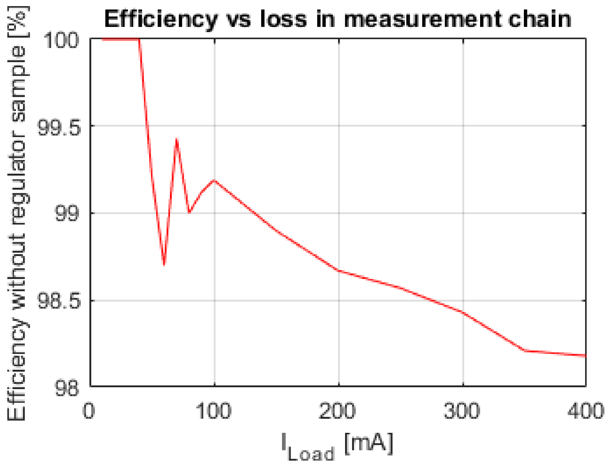
Before each efficiency measurement, an offset was evaluated. This offset represents the deviation of true efficiency η due to power losses in the measurement chain (between INA219 and load), as is shown in Figure 11.
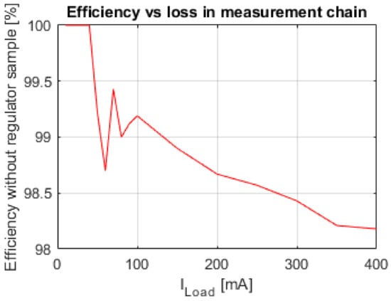
Figure 11.
Efficiency vs. loss in measurement chain.
The offset was determined when output port −Vin of the first INA219 was directly connected (without a regulator) to input port +Vin of the second INA219 module, as is shown in Figure 8.
Voltage = 5 V was connected to the +Vin port of the first INA219, and current = 490 mA flowed through the INA219 module to the 10 Ohm load resistor. The difference between input and output power was not zero, because the INA219 development board measured its efficiency as approximately 98%. When the load resistor was changed to 22 Ohms, the load current was 225 mA and the measured efficiency reached 98.6%.
As seen in Figure 11, the true efficiency is approximately 1–2% higher than the efficiency values displayed on the OLED display but only for currents more than 0.1 A up to 0.5 A. When a load resistance is higher than 100 Ohms (load current lower than 50 mA), the measurement chain error is zero (100% efficiency is displayed).
4.2. Comparison of Regulators Noise Performance by Fast Allan Variance Method
Noises are stochastic errors that are important in various applications [20,21], where characteristic noises, a white noise, or bias instability (flicker noise) have a big impact on sensor output or power supplies’ voltage values.
According to the theoretical analysis in the introduction, there is the possibility to use a similar principle for the noise analysis of power supplies as was used in inertial sensor technology [16].
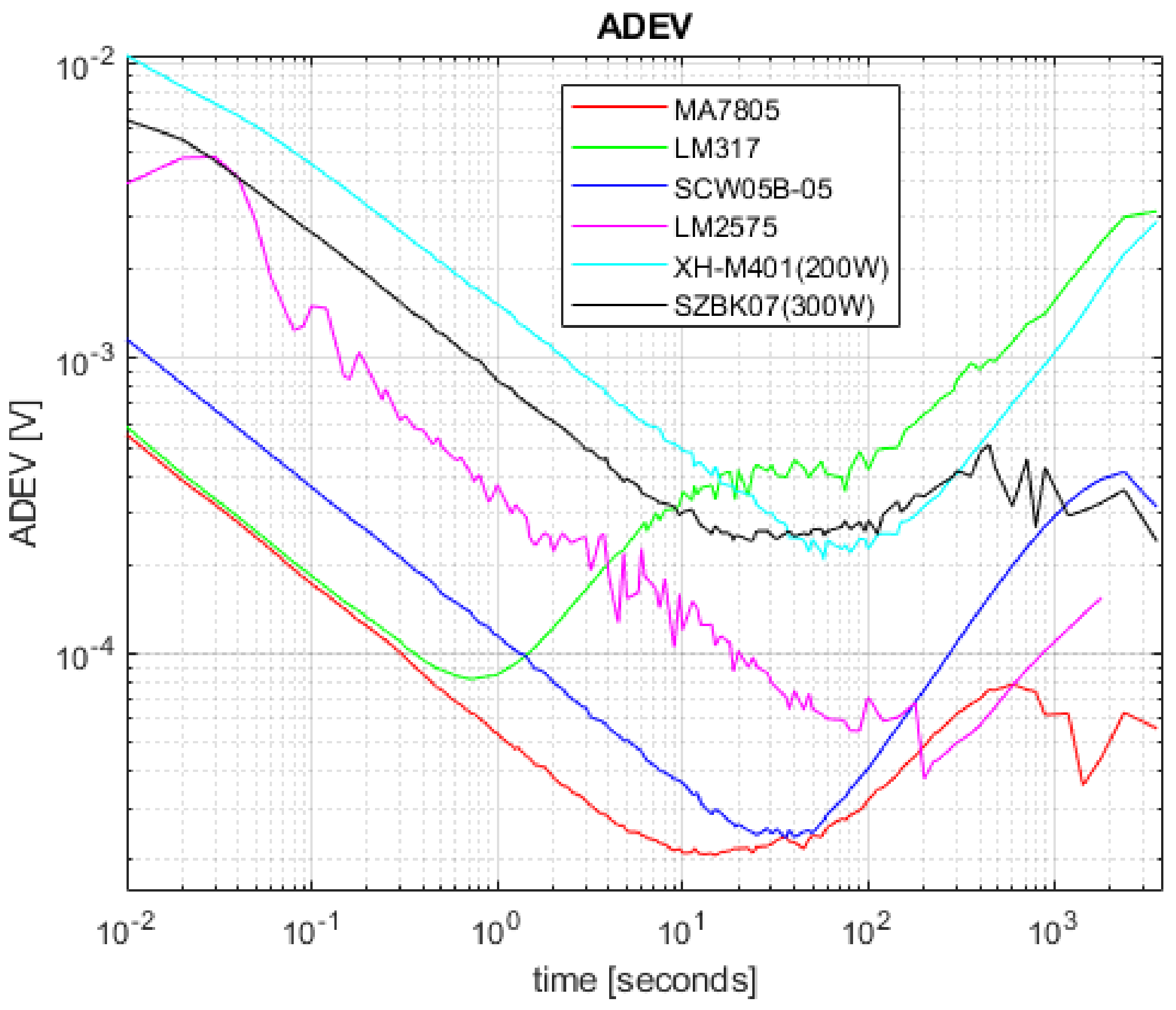
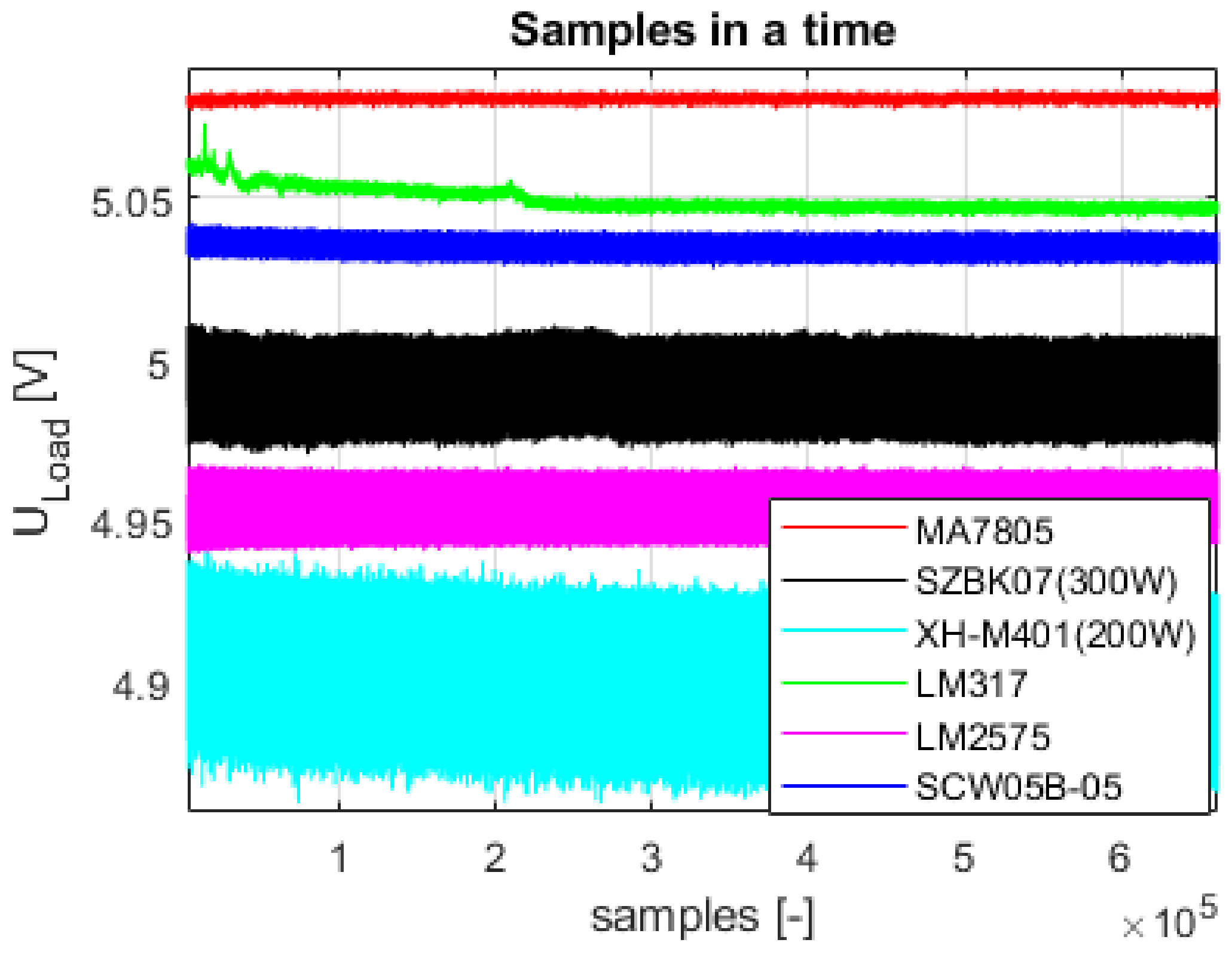
As can be seen in Figure 12, Allan deviation (ADEV) (square root of AVAR) was computed according to (7) from N = 720,000 measurement samples of (at the sampling frequency 100 Hz, see Figure 13) for all regulator samples.
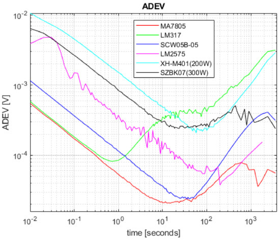
Figure 12.
Allan curves of regulator samples.

Figure 13.
Output voltage of regulators samples.
For the computation of ADEV, algorithm (7) implemented in a MATLAB 9.13.0.2502115 (R2022b) Update 8 environment was used:
N = 720000; % number of measurement samples
prime_factor = factor(N); % calculation of prime factor
unique_factor = unique(prime_factor); % sorting without repetition
hist_fact = histc(prime_factor,unique_factor); % histogram count
vector = (unique_factor(1)).^(0:hist_fact(1));
for i = 2:length(unique_factor)
fact = unique_factor(i);
K = fact.^(0:hist_fact(i));
vector = kron(vector,K); % Kronecker tensor
end
div = sort(vector); % ascending order sorting
K = length(div); % number of divisors
meas = A(1:N,1); % load measurements
for i = 1:1
Z = zeros(div(i),N/div(i)); % zeros matrix
Z = reshape(meas,div(i),N/div(i));% reshape
avarZ = zeros(1,N/div(i)-1); % zeros matrix
for n = 1:N/div(i)-1
avarZ(1,n) = (Z(n + 1)-Z(n))^2;
end
avar_1 = (0.5*sum(avarZ))/(N/div(i)-1);
adevZ(1,i) = sqrt(avar_1);
end
for i = 2:length(div)-1
Z = zeros(div(i),N/div(i)); % zeros matrix
Z = reshape(meas,div(i),N/div(i)); % reshape “meas”
avarZ = zeros(1,N/div(i)-1); % zeros matrix
avgZ = mean(Z); % mean computation
for n = 1:N/div(i)-1
avarZ(1,n) = (avgZ(n + 1)-avgZ(n))^2;
end
avar_1 = (0.5*sum(avarZ))/(N/div(i)-1); % AVAR computation
adevZ(1,i) = sqrt(avar_1); % ADEV computation
end
div_interval = div(1:length(div)-1); % Corellation time τ(tau)
loglog(div_interval/100,adevZ) % figure plot
title(‘Allan Deviation’) % title of ADEV
xlabel(‘Time [seconds]’) % x-axis label
ylabel(‘Allan Deviation [V]’) % y-axis label
grid on
The ADEV of each of the regulator samples has a characteristic Allan curve shape as in [13,16], where it is possible to divide each regulator curve into the following two regions:
- region of low correlation time;
- region of long correlation times.
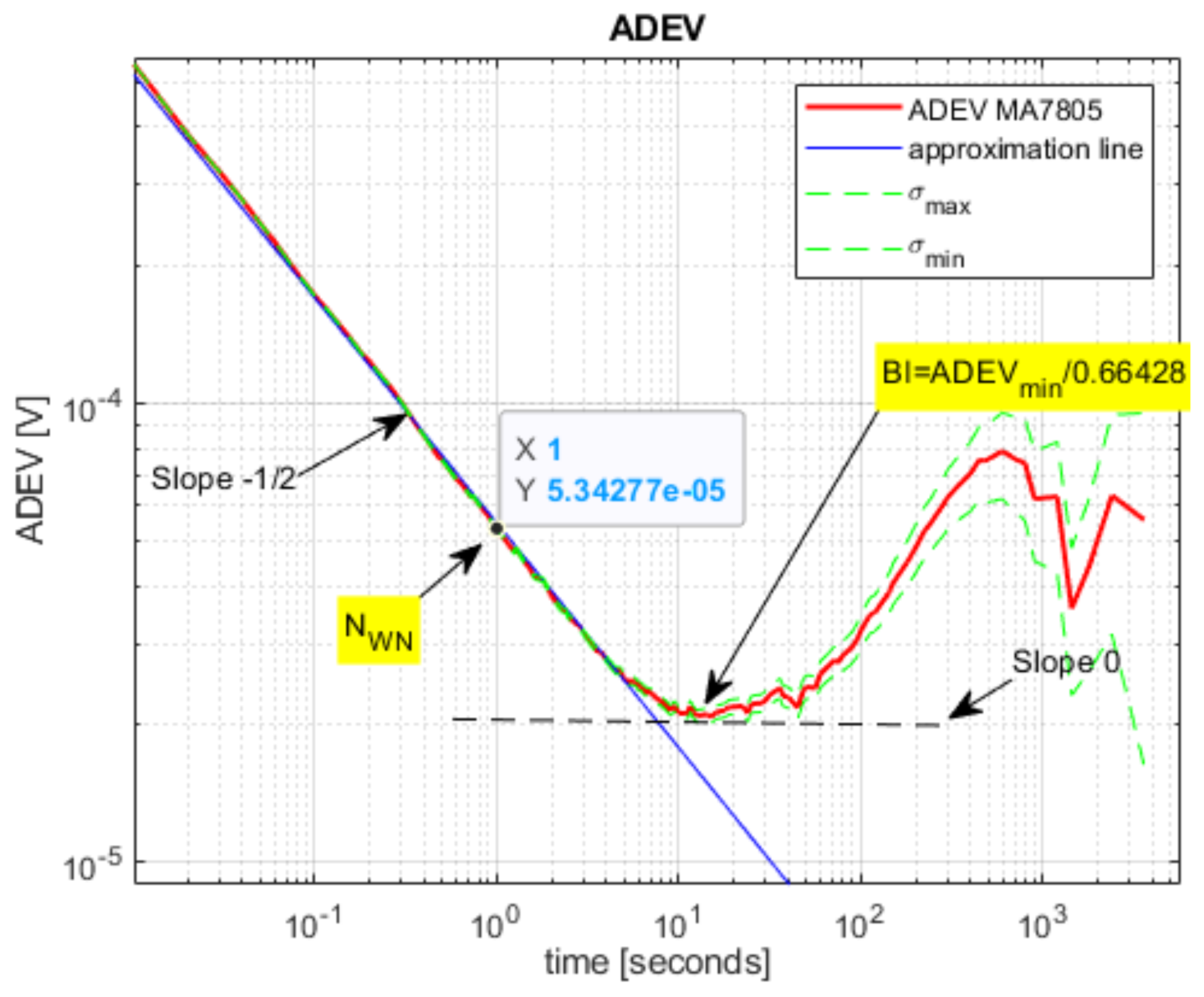
In the low correlation time region (see Figure 14) it is possible to estimate white noise (WN) coefficients NWN and bias instability coefficients BI.
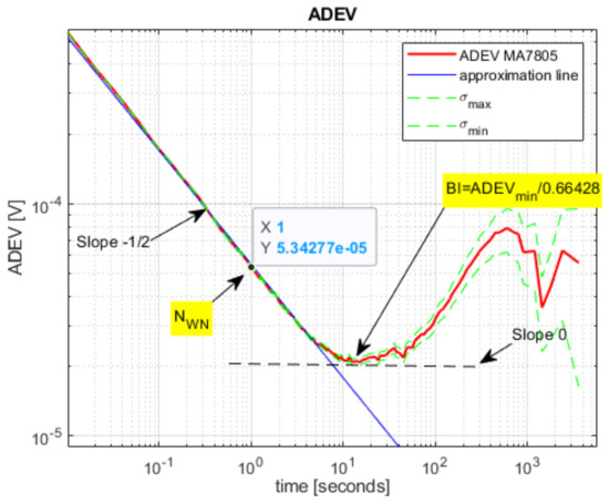
Figure 14.
Noise coefficient estimation and confidence intervals.
The result ADEVs (Figure 14) were computed according to (7) and (8). Characteristic noise coefficients and BI with their errors according (9) and (10) were computed and are listed in Table 3.
Table 3.
Comparison of the PWM switching regulator topologies.
According to the Allan variance method used, Figure 12, Figure 13 and Figure 14, and the resulting noise coefficients and the following conclusions can be stated:
- linear regulators MA7805, LM317 are characterized by much lower white noise (coefficient) values (in some cases the difference is 10 fold).
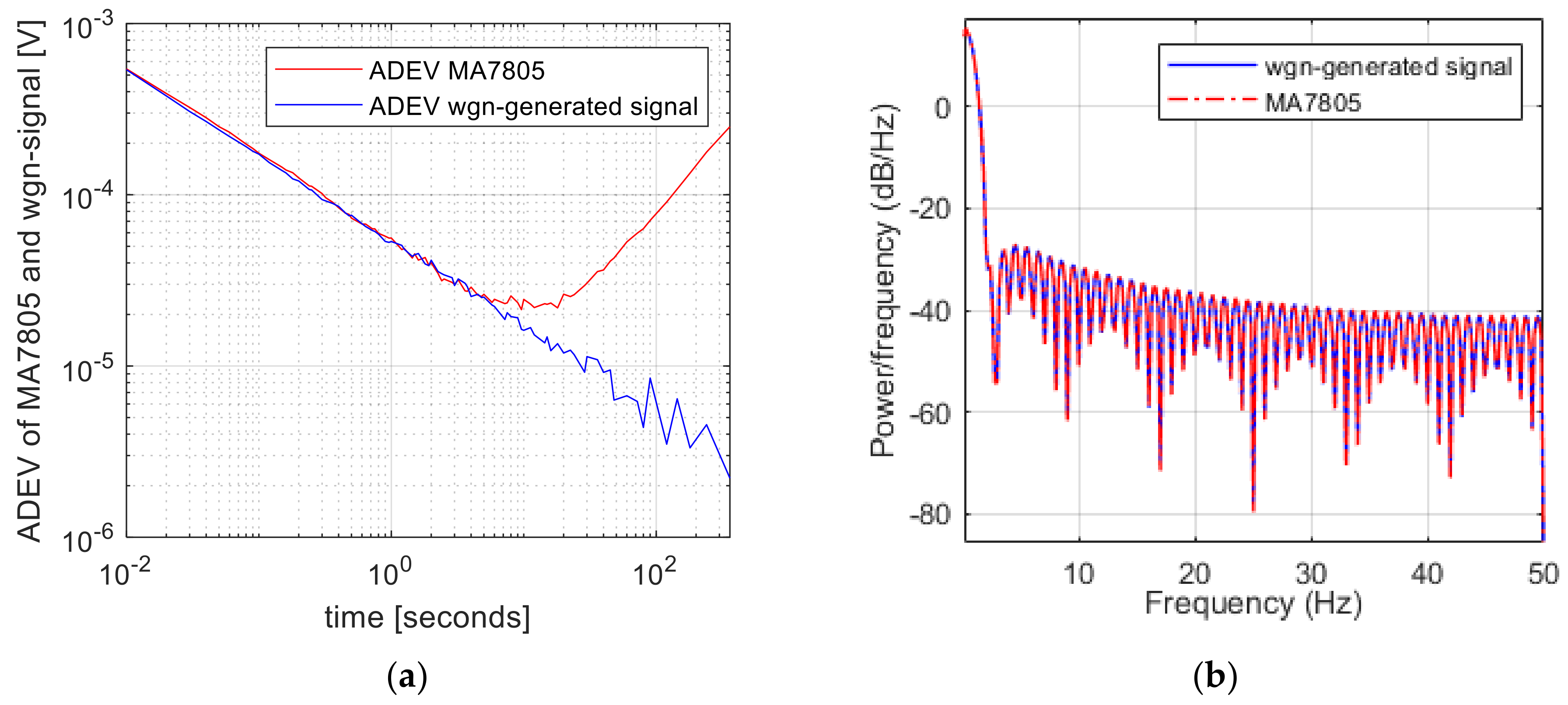
White noise values of linear and switching regulators can be generated in MATLAB according to the corresponding NWN from Table 3. The command is used, where white noise generator power in decibels is determined according to the following equation:
where is a power spectral density of white noise and the bandwidth 100 Hz. Seed is the white noise generator initial value in which the white noise generator starts the generation of values with a specific .
A comparison of MA7805 regulator measured values and wgn-generated values in MATLAB is shown in Figure 15a. Here, it can be seen that the white noise of a real MA7805 linear regulator and the generated wgn-values (based on coefficient) are similar in the first region of the ADEV curve. In the same way, of the linear regulator MA7805 and of the wgn-generated noise in Figure 15b are the same.
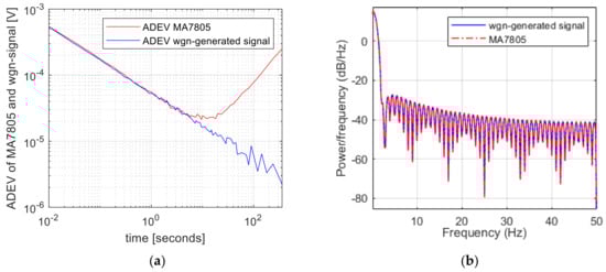
Figure 15.
(a) ADEV, (b) of the MA7805 and wgn-generator output values.
5. Discussion
This article presents linear regulator and switching regulator efficiency measurements and noise evaluation at regulator outputs where the fast Allan variance method was used. In each section of the article, an evaluation of the measured results and an assessment of them against the manufacturer’s data is presented. In the context of comparing the values of the achieved efficiencies, in this section the authors summarize all the significant main results.
According to the developed measurement site (based on the embedded system Arduino UNO and INA219 circuits) in Section 4 (Measurement results), it was possible to determine efficiency values for linear and switching regulators according to the theoretical analysis presented in Section 3. (Methodology and analysis). The efficiency of linear regulators is relatively lower in comparison with the switching regulator examples. However, for low load currents in switching regulators, lower efficiency values were found compared with the expected (maximum) values defined by their producers [6,7,8,9,10,11]. Based on the experimental results, the selection of a suitable regulator must be realized according to assessment load current ranges in connection with achievable efficiency values. The results presented in Section 4 lead to the statement that switched regulators are replaceable by linear regulators but only for currents approx. up to 10 mA.
In real measurements of parameters, voltage, current and power, there will always be errors caused by the used method of measuring efficiency, which in this case reached 1–2%. However, with larger currents, the percentage measurement errors will increase. It is also necessary to consider the static and dynamic errors of the ADC.
The limitation of the chosen method of determining the efficiency of the regulators in practice depends on a specific measuring workplace, where in this specific case it was possible to determine the efficiency for input voltages up to 26 V and currents to the regulators up to a maximum of 3 A.
However, INA219 provides considerable flexibility regarding the choice of shunt resistor size. Based on the shunt resistor selection, it is possible to narrow or extend the current (power) measurement range. In this way, we can increase or decrease the resolution of the measured current or power. To increase the reliability and accuracy of measuring the parameters of power supplies (to determine their efficiency), it is advisable to use statistics methods, averaging several tens to hundreds of measurements per second for the elimination of ADC errors arising during analogue–digital conversion.
If we talk about the Allan variance method, especially the fast Allan variance method, this is a method that uses a nonoverlapped cluster sampling technique for the Allan deviance (Allan curve) computation. The nonoverlapped cluster sampling technique used in our innovative algorithm is characterized by a very fast computation speed and by acceptable characteristic noise coefficient percentage errors. Because, generally, this method is widely used in different areas of research (radio electronics, astronomy, inertial navigation, and others) this method can used for setting errors in power supply sensitive applications. These errors created by a specific power supply (regulator) can be used for the classification of the regulators from the point of view of a specific application.
6. Conclusions
Key parameters of linear and switching power supply regulators are input/output voltages (currents), efficiency , line regulation, load regulation, output ripple, noise, and others.
In this article, a division of linear and switching power supply regulators is described, including their basic advantages, and disadvantages. The article describes the design of an efficiency measurement site based on INA219 power monitors and the Arduino UNO embedded system. According to measurements with linear regulators MA7805, LM317, switching regulators SZBK07, LM2575, SCW05B-05, and XH-M401, their efficiency values in low-and-high current regions were analyzed. Efficiency determination errors in the measurement chain were evaluated and they did not exceed 1–2%.
For evaluation of noise performance of regulators, we used the Allan variance method (AVAR). This method is universally applicable for various physical quantities and instability determination (e.g., noise performance). Noise performance evaluation was focused on white noise and bias instability (flicker noise estimation). According to estimated white noise coefficient values, it was possible to generate the corresponding output signal in MATLAB. Regulator output measured signal and wgn-generated signal noise performance were compared.
The above-mentioned ADEV-MATLAB script based on the fast AVAR method allows (in contrast with methods used in [12]) us to achieve an extremely short ADEV computation time. For example, a 7.2 Mega sample (MSa) file can be processed in up to 1 s and a 72 MSa file in up to 11 s. Therefore, this fast ADEV algorithm is excellent for big data sets.
Thanks to the high speed of the AVAR algorithm execution, there is a possibility to use this fast AVAR method (among other things) for online-sensing diagnostics of a power source’s condition and for powered sensors and devices, making it possible to avoid or predict malfunctions in various instruments.
Author Contributions
Conceptualization, M.M.; methodology, M.M.; software, M.M.; validation, M.Š.; formal analysis, M.Š.; investigation, M.M.; resources, M.M. and M.Š.; writing—original draft preparation, M.M. and M.Š.; writing—review and editing, M.Š. All authors have read and agreed to the published version of the manuscript.
Funding
This research received no external funding.
Data Availability Statement
Data are contained within the article.
Conflicts of Interest
The authors declare no conflicts of interest.
References
- Rozenblat, L. Switching Power Supply Design: A Concise Practical Handbook; Lulu.Com: Seiten, Kazakhstan, 2021; ISBN 978-1-71612-745-8. [Google Scholar]
- Billings, K.H.; Morey, T. Switchmode Power Supply Handbook, 3rd ed.; McGraw-Hill: New York, NY, USA, 2011; ISBN 978-0-07-163972-9. [Google Scholar]
- Pressman, A.I.; Billings, K.H.; Morey, T.; Billings, K. Switching Power Supply Design, 3rd ed.; McGraw-Hill: New York, NY, USA, 2009; ISBN 978-0-07-148272-1. [Google Scholar]
- Lakota, B. Power Supplies I, 1st ed.; Armed Forces Academy of general Milan Rastislav Štefánik: Liptovský Mikuláš, Slovakia, 2007; ISBN 978-80-8040-337-9. [Google Scholar]
- Brown, M. Power Supply Cookbook, 2nd ed.; EDN Series for Design Engineers; Newnes: Boston, MA, USA, 2001; ISBN 978-0-7506-7329-7. [Google Scholar]
- STMicroelectronics. Positive Voltage Regulator ICs L78 Series; DS0422, Rev 36, 9/2018. Available online: https://www.st.com/resource/en/datasheet/l78.pdf (accessed on 19 April 2024).
- Texas Instruments. LM117, LM317-N Wide Temperature Three-Pin Adjustable Regulator, SNVS774Q, 5/2004, REVISED 6/2020. Available online: https://www.ti.com/lit/ds/symlink/lm317-n.pdf (accessed on 19 April 2024).
- Texas Instruments. LM5116 Wide Range Synchronous Buck Controller, SNVS499I, 2/2007, REVISED 11/2023. Available online: https://www.ti.com/lit/ds/symlink/lm5116.pdf (accessed on 19 April 2024).
- Mean Well. SCW05B-05, 5W DC-DC Regulated Single Output Converter SCW05 Series, SCW05-SPEC, 3/2008. Available online: https://www.micro-semiconductor.com/datasheet/f5-SCW05A-12.pdf (accessed on 19 April 2024).
- Texas Instruments. LM2575 1-A Simple Step-Down Switching Voltage Regulator, SLVS569F, 1/2005, REVISED 8/2015. Available online: https://www.ti.com/lit/ds/symlink/lm2575.pdf (accessed on 19 April 2024).
- XLSEMI. 8 A 180 kHz 40 V Buck DC to DC Converter XL4016, Rev 1.2. Available online: https://www.makerfabs.com/desfile/files/XL4016-Datasheet.pdf (accessed on 19 April 2024).
- Li, J.; Fang, J. Not Fully Overlapping Allan Variance and Total Variance for Inertial Sensor Stochastic Error Analysis. IEEE Trans. Instrum. Meas. 2013, 62, 2659–2672. [Google Scholar] [CrossRef]
- Draganová, K.; Kmec, F.; Blazek, J.; Praslicka, D.; Hudak, J.; Laššák, M. Noise Analysis of Magnetic Sensors Using Allan Variance. Acta Phys. Pol. A 2014, 126, 394–395. [Google Scholar] [CrossRef]
- Allan, D.W. Statistics of Atomic Frequency Standards. Proc. IEEE 1966, 54, 221–230. [Google Scholar] [CrossRef]
- IEEE Std 1139-2008; IEEE Standard Definitions of Physical Quantities for Fundamental Frequency and Time Metrology—Random Instabilities. Re-vision of IEEE Std 1139-1999. IEEE: Piscataway, NJ, USA, 2009; pp. 1–50. [CrossRef]
- Matejček, M.; Šostronek, M. New Experience with Allan Variance: Noise Analysis of Accelerometers. In Proceedings of the 2017 Communication and Information Technologies (KIT), Tatranské Zruby, Slovakia, 4–6 October 2017; pp. 101–104. [Google Scholar] [CrossRef]
- El-Sheimy, N.; Hou, H.; Niu, X. Analysis and Modeling of Inertial Sensors Using Allan Variance. IEEE Trans. Instrum. Meas. 2008, 57, 140–149. [Google Scholar] [CrossRef]
- Texas Instruments. INA219 Zerø-Drift, Bidirectional Current/Power Monitor with I2C Interface, SBOS448G, 8/2008, REVISED 12/2015. Available online: https://www.ti.com/lit/ds/symlink/ina219.pdf (accessed on 19 April 2024).
- Matejček, M.; Šostronek, M. Arduino Programming in Examples (Arduino Programovanie v Príkladoch); Armed Forces Academy of general Milan Rastislav Štefánik: Liptovský Mikuláš, Slovakia, 2023; ISBN 978-80-8040-649-3. [Google Scholar]
- Soták, M. Integrated Navigation System—System Design and Implementation of Algorithms in Real Time. Habilitation Thesis, Technical University of Košice, Košice, Slovakia, 2011. [Google Scholar]
- Krivanek, V. Application LAMDA Algorithm for Fault Detection and Isolation. In Proceedings of the 14th International Conference Mechatronika, Trencianske Teplice, Slovakia, 3–6 June 2011; pp. 46–51. [Google Scholar] [CrossRef]


Disclaimer/Publisher’s Note: The statements, opinions and data contained in all publications are solely those of the individual author(s) and contributor(s) and not of MDPI and/or the editor(s). MDPI and/or the editor(s) disclaim responsibility for any injury to people or property resulting from any ideas, methods, instructions or products referred to in the content. |
© 2024 by the authors. Licensee MDPI, Basel, Switzerland. This article is an open access article distributed under the terms and conditions of the Creative Commons Attribution (CC BY) license (https://creativecommons.org/licenses/by/4.0/).