Abstract
Despite the extensively researched physical principles, numerous published simulations on SiC drift step recovery diodes (SiC DSRD) and the practical implementation of SiC DSRD-based pulses, there are few kinds of research focusing on collaborative design between a SiC DSRD and its driving circuit. In this paper, a collaborative design method of a SiC DSRD and its driving circuit are presented. In addition, a detailed simulation is conducted to verify design considerations and to analyze the impact of driving parameter changes on the output pulse waveform. A pulse generator prototype with a self-developed SiC DSRD is implemented. The experimental results show that the circuit can output a peak voltage of 790 V on a matching load of 50 Ω, with a rise time of 520 ps (20%~80%), and can work at a 1 MHz repetition frequency rate with good stability.
1. Introduction
Pulsed power technology is a method that compresses energy from milli- or microseconds to nano- or picoseconds on the time scale and brings several orders of magnitude increase in the power level. This technology finds extensive applications across various industries such as food processing, nitric oxide production, water and exhaust gas treatment, and ion implantation, among others [1]. Numerous experiments have demonstrated that nanosecond pulses are particularly advantageous for these applications [2,3,4]. While conventional semiconductor switches like IGBTs, MOSFETs, and thyristors can effectively generate microsecond power pulses in such scenarios, they are not suitable for generating high-voltage nanosecond pulses. To address this issue, drift step recovery diodes (DSRDs) can be employed [5].
Drift step recovery diodes (DSRDs), as a new type of semiconductor opening switch, can generate a nanosecond pulse on the load through a matching external trigger circuit. However, the DSRD has strict requirements for circuit matching. The unmatched driving circuits will lead to a decrease in the output peak, the slowdown of the pulse front, and an increase in power loss owing to the appearance of pre-pulse.
Based on DSRD devices, a number of scholars have reported extensive research. The Russian Ioffe Physical-Technical Institute developed a pulsed generator with a front edge of 600 ps and an amplitude of 2 kV [6]. Israel’s Soreq Nuclear Laboratory presented a solid-state pulsed generator with a front edge of less than 1 ns and an amplitude of 6 kV [7]. The American SLAC National Accelerator Laboratory reported a pulsed power supply. The rise time was less than 2 ns and the amplitude was 15 kV based on the DSRD front-end pump circuit [8,9]. The Northwest Institute of Nuclear Technology in China developed a pulsed generator with a pulse front of 700 ps and an amplitude of 2 kV [10]. In 2016, V.A. Ilyin et al. reported the circuit test results of an eight-diode-stacked 4H-SiC DSRD device with the P+PN+ structure. The rise time of the output pulse was 900 ps with an amplitude of 10.5 kV and verified the possibility of stacking 4H-SiC DSRD devices for the first time [11]. In the same year, B.V. Ivanov et al. reported the results of the repetition frequency operation test of a single diode P+PN+ structure. The rise time of the output pulse was 500 ps with an amplitude of 1.8 kV and a maximum repetition frequency of 500 kHz [12]. In 2018, T Goto et al. from Tsukuba University of Japan prepared a SiC DSRD with a P+PNN+ structure. It is different from the conventional P+PNN+ structure. In conventional P+PNN+ structure, the P-type base region stores plasma, and the N-type base region bears pressure. However, based on the result of the simulation, T Goto et al. found that the 9 μm thick P-type base region matches the 8 μm thick N-type base region when the pulse generator output voltage is the largest and the rise time is shorter. After stacking five diodes, the rise time of the output pulse was 2.3 ns with an amplitude of 11 kV [13]. In addition, V.A. Ilyin et al. reported the test results of 15 diodes stacked with a 4H-SiC DSRD, with an output pulse rise time of 1.6 ns and an amplitude of 30.5 kV [14]. In the same year, Wang Yajie et al. reported a pulse generator with an output pulse amplitude of 2 kV and a pulse front of 680 ps (20%~90%). Based on the equivalent model of DSRD, the simulation model of the forward-and-reverse pump circuit is established. According to the requirements of output voltage, the values of energy storage inductance are simulated and analyzed. Finally, optimal values of the component parameters in the circuit are obtained [15]. In 2020, Sun Ruize et al. reported a SiC DSRD device with the P+PNN+ structure, in which the breakdown voltage was above 10.9 kV. The measured output pulse rise time was 1.75 ns with an amplitude of 10.56 kV, and the maximum repetition frequency was 1 MHz [16]. In 2021, Liang Lin et al., from Huazhong University of Science and Technology of China, reported the testing results of a SiC DSRD circuit using four-way parallel triggering. The measured rise time of the output pulse was 1.011 ns, and the amplitude was 2.302 kV. By adjusting the DC bias voltage of the input circuit, they found that the amplitude and rise time of the output voltage of the device increase with the increase in the DC bias voltage [17].
Although the match between a DSRD and its driving circuits is an important issue, little research pays attention to the collaborative design of DSRD and its driving circuits. In this paper, a collaborative design method of a SiC DSRD and its driving circuit are presented. In addition, a detailed simulation is conducted to verify design considerations and to analyze the impact of driving parameter changes on the output pulse waveform. A pulse generator prototype with self-developed SiC DSRD is implemented.
2. Design of SiC DSRD Device
2.1. Operation Principle of SiC DSRD
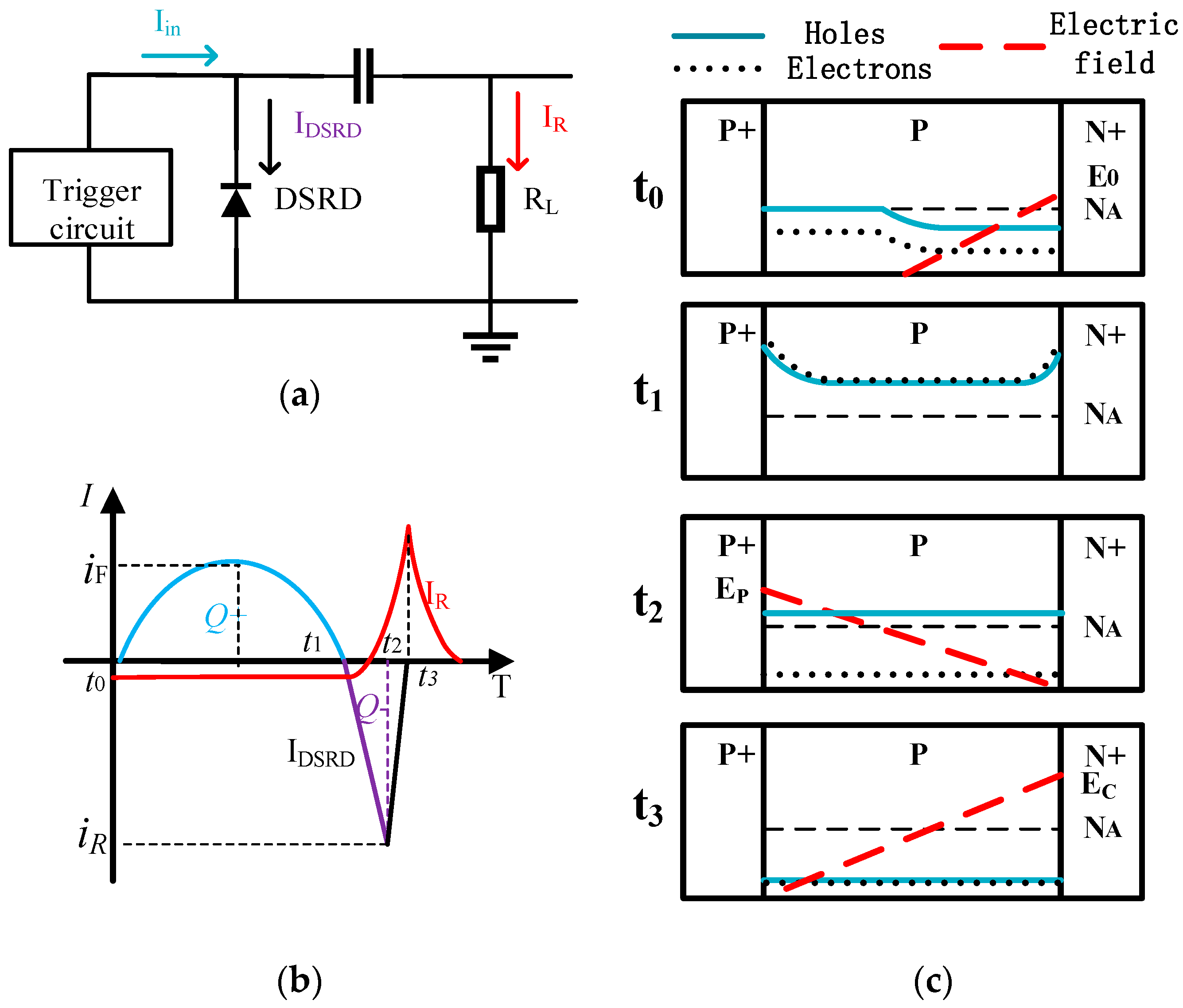
A simplified operating circuit is shown in Figure 1a. The DSRD is connected in parallel to the load. The waveform of input current Iin is shown in Figure 1b. Id and Iout are the currents flowing through the DSRD and the load, respectively. When the DSRD is turned off, Iin is switched from the the DSRD loop to the load loop, then forms a high-voltage fast pulse on the load (RL).
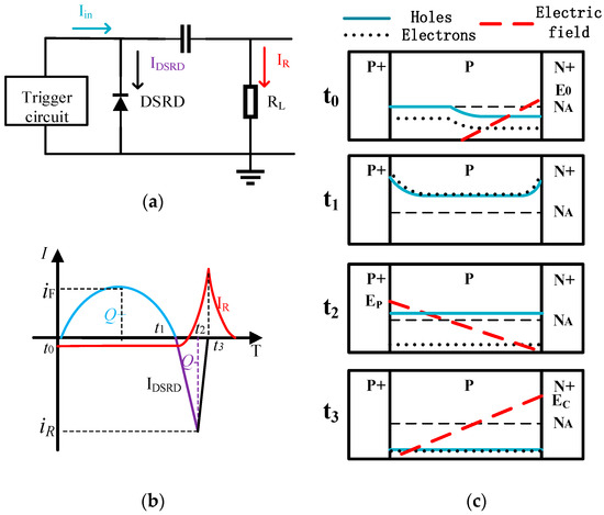
Figure 1.
The working principle of DSRD: (a) the simplified working circuit of DSRD; (b) switching characteristics of DSRD; (c) the carrier concentration and electric field distributions at different times.
Figure 1c shows the carrier concentration and electric field distributions at different times. Initially, the DSRD is in the blocking state due to the existence of the space charge region (SCR). Before t0, the hole concentration and doping concentration are basically the same in the base region, whereas the electron concentration can be ignored. Then, Iin provides a forward current to the DSRD. Electrons and holes, from the N+ region and P+ region, are injected into the base region. It decreases the resistance of the base region. During the t1-t2 process, the current Iin changes direction into reverse to extract the plasma in the base area. The resistance of the base region is still low due to the existence of high-concentration plasma. At time t2, the plasma is completely extracted, and the reverse current reaches the maximum. At this moment, the majority of carriers are extracted by the reverse current Iin and move with the saturated velocity. Meanwhile, the space charge region forms at the PN+ junction and expands with the speed of saturated velocity. As a result, the resistance of the base region sharply increases, and the current switches from the DSRD to the parallel connected load with the output pulse. At time t3, the space charge region is completely established, and the output pulse reaches its maximum voltage.
In addition, for SiC DSRDs, vast loss of injected charge is a general issue [18,19] which may lead to a decrease in DSRD energy efficiency. The charge loss rate is defined as Q-/Q+. The extracted non-equilibrium charge Q- and injected charge Q+ are defined by the areas under current transient response at different stages of the recovery process of the DSRD [20].
2.2. Parameter Selection and Optimization of SiC DSRD
It is worth noting that, in the process of plasma extraction, if the carrier concentration at the base region cannot sustain the reverse current, major carriers will accumulate at the border of the P+P junction [21]. In this case, the voltage drop on the base will occur before the cutoff, resulting in the appearance of pre-pulse. It increases the power loss of the DSRD. To avoid the appearance of the pre-pulse, in terms of the DSRD design, the maximum reverse current (Imax) must satisfy the following:
In Equation (1), q is the elementary charge quantity; NA is the base doping concentration; vs is the carrier-saturated drift velocity of the base region; and S is the active area of the DSRD.
In addition, the breakdown voltage (VBV) of the DSRD is the main parameter that restricts the output peak voltage (Vmax) of the pulse generator. In other words, VBV puts an upper limitation on the output peak current. The DSRD breakdown voltage VBV can be expressed as
The output peak voltage Vmax is
The relation between VBV and Vmax is
Therefore, the Imax is limited by NA and W, as shown in Equation (6):
In Equations (2) and (3), W is the base width; RL is the load resistance which is usually 50 Ω.
Then, the suitable structure parameter of DSRD can be determined. At first, the Imax value or Vmax value will be given in advance according to practical requirements. Next, the value of the W, NA, and S can be chosen based on Equations (1) and (6). That is to say, when one of the three parameters is given, the other two parameters will also be obtained. For example, in this paper, the given Vmax value is 800 V. Based on the given design method, a SiC DSRD is designed. The thicknesses of the p+ and p-base layers are 2 μm and 6 μm, with accepted concentrations of 1 × 10¹⁹ and 2 × 1016 cm−3, respectively; the n+ layer has a thickness of 5 μm and a doping concentration of 1 × 1019 cm−3. The active area S is 0.28 mm2.
3. Collaborative Design of DSRD-Based Pulse Generator
3.1. Working Principle of Driving Circuit
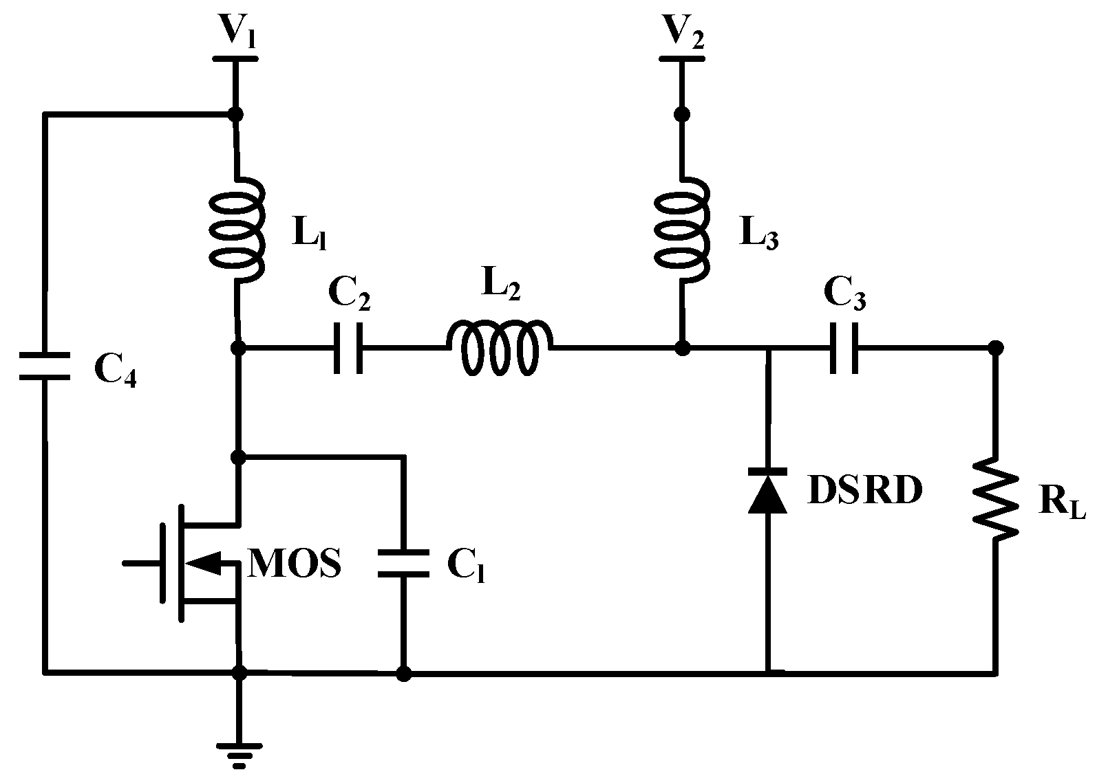
The schematic diagram of the driving circuit of the DSRD is illustrated in Figure 2. which consists of two DC power supplies with voltage V1 and V2, the primary switch of SiC MOSFET(MOS), energy storage inductances L1 and L2, the decoupling capacitance C1, the resonant capacitance C2, the dc-blocking capacitance C3, the decoupling capacitance C4, the DSRD device, and the load RL.
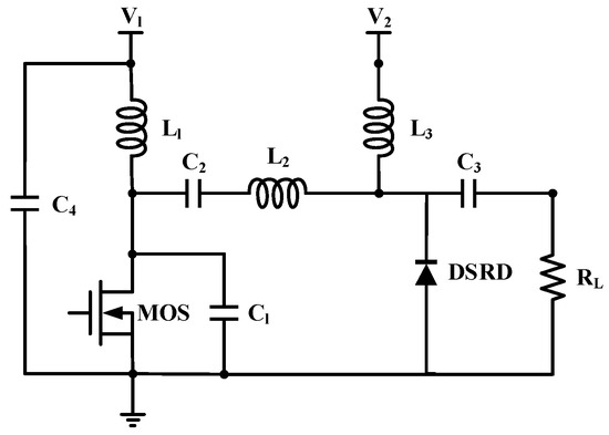
Figure 2.
Schematic diagram of DSRD-based pulse generator.
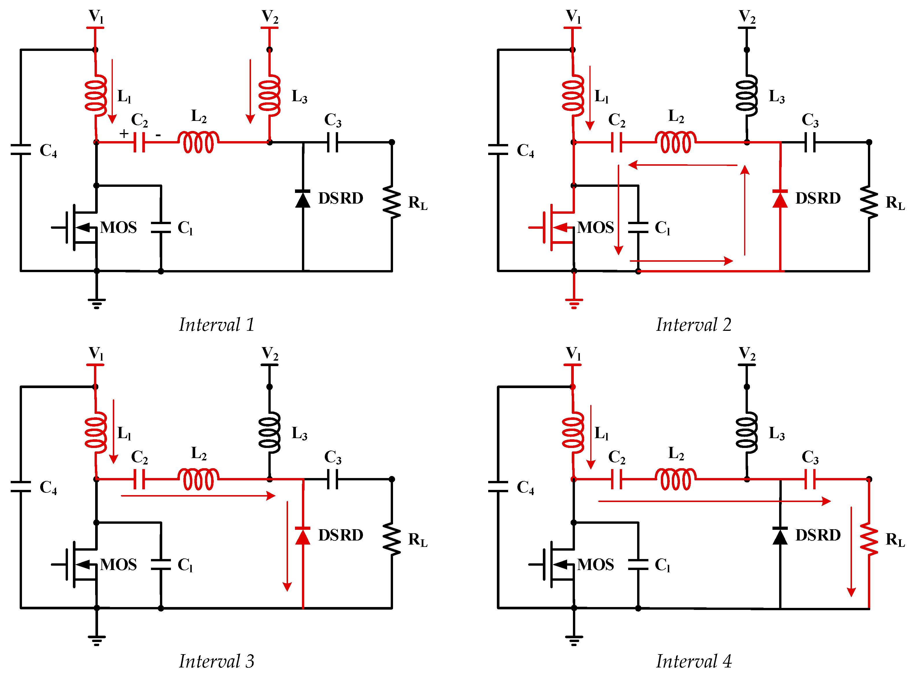
The working process can be divided into four intervals, which are shown in Figure 3. Figure 4 shows the current waveforms during the operation.
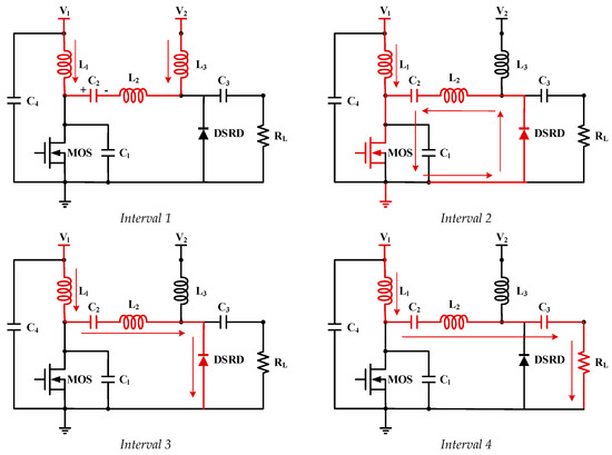
Figure 3.
Equivalent circuit of pulse generator.
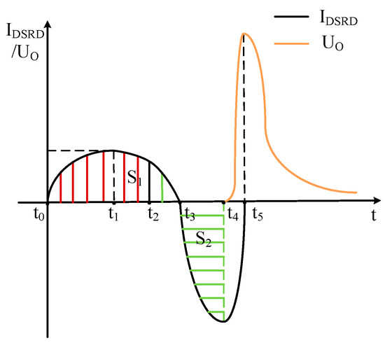
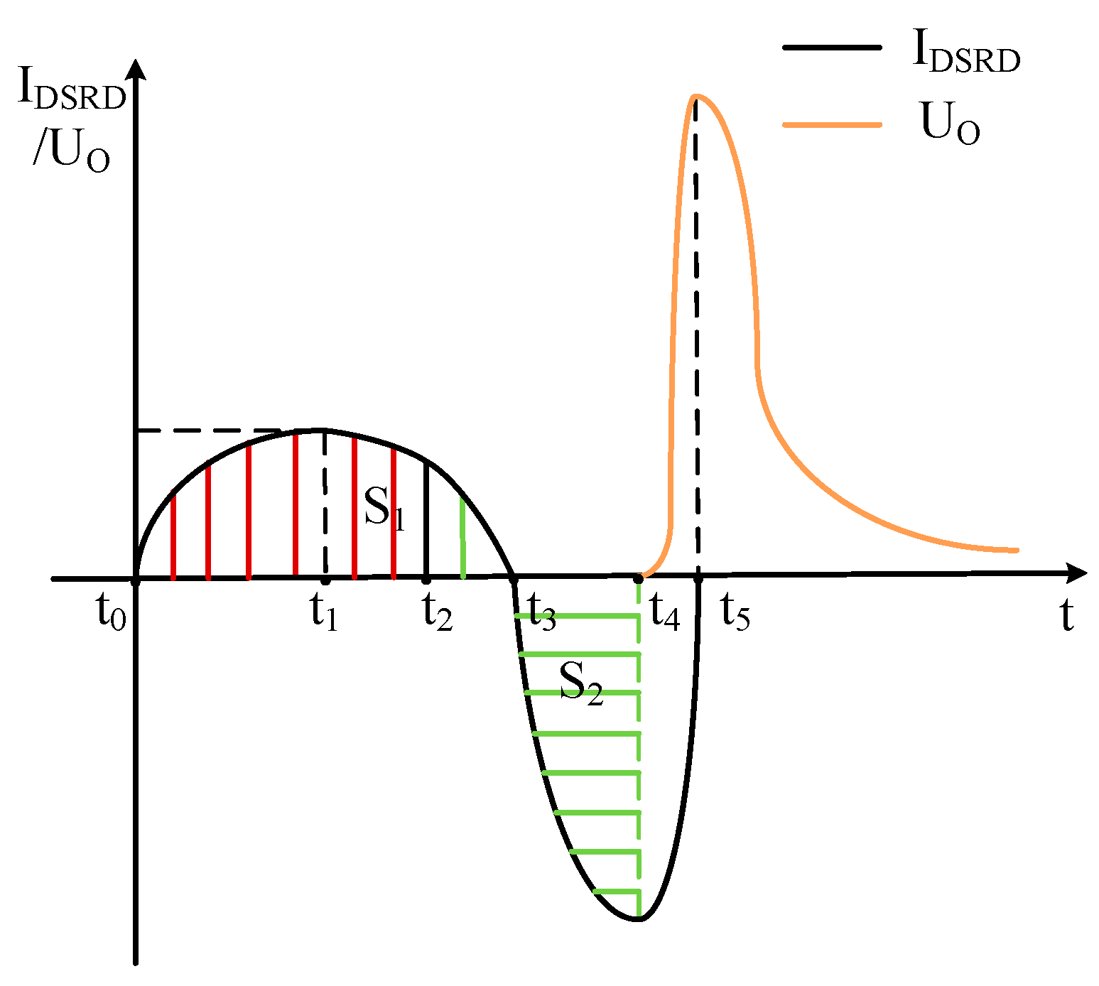
Figure 4.
Theoretical waveforms in the circuit shown in Figure 3.
Interval 1: Initially, the MOS is off-state, and the resonant capacitance C2 is charged by V1 and V2 to the initial voltage .
Interval 2: At t0, the MOSFET is turned on; then, the circuit can be divided into two loops, which are V1-L1-MOSFET(loop1) and C2-MOSFET-DSRD-L2(loop2). In loop1, the inductor L1 stores the energy from V1, and the current of L1 can be expressed as
In loop2, the inductor L2 and capacitor C2 begin to resonate, and at t1 the resonant current reaches its peak value, then it begins to decrease. The resonant current which can be considered as the forward current accumulates charge carriers in the DSRD; the resonant current can be expressed as
Interval 3: At t2, the MOSFET turns off. The energy stored in L1 needs to be released through C2, L2, and DSRD. Then, the resonant current decreases rapidly. At t3, the resonant current reverses. During the interval, the resonant current extracts charged plasma which has been accumulated in interval 2.
Interval 4: At t4, the plasma in the DSRD base region is depleted by the extracting process, and the DSRD is rapidly turned off. Then, the high current through the DSRD is swiftly switched to the load RL, generating a high-voltage pulse.
3.2. Conduction Time of the MOSFET
In order to weaken the effect of carrier recombination, the charge carrier’s accumulation process in DSRD should satisfy the following equation:
where ΔT represents the conduction time of the MOSFET, represents the carrier lifetime of the SiC DSRD, which equals 40 ns. Therefore, the conduction time ΔT is selected as 25 ns.
3.3. Inductance Design
The inductors used in power pulse technology often require a wide frequency response. Due to the easy saturation and large inductance deviation under different frequencies of the magnetic core inductor, the hollow inductor is selected in this design.
Based on the working principle illustrated above, the high-voltage pulse is generated by the high current through the DSRD swiftly switched to the load RL. During the voltage pulse output, the current of L2 can be expressed as
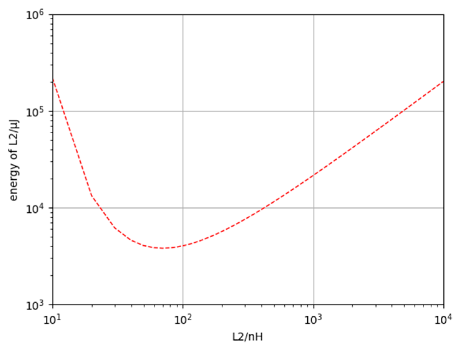
The energy stored in the inductor L2 can be expressed as
Based on (11), the relationship between the value of L2 and its stored energy is shown in Figure 5.

Figure 5.
Energy varies with the value of L2.
It can be seen that when the L2 equals 75 nH, the energy stored in L2 reaches its maximum value. In practice, the L2 is selected as 100 nH.
In order to ensure that the designed inductance works in the linear region, the maximum current of L1 is selected as iL1-max = 9.5 A. Therefore, the inductance of L1 can be calculated as
Based on (12), when ΔT = 25 ns, V1 = 120 V, and iL1-max = 9.5 A, L1 = 320 nH is selected. Table 1 shows the selected circuit parameters.

Table 1.
Pulse generator parameters.
3.4. Capacitance Design
During the interval2, in circuit loop2, the on-resistance of MOSFET (RDSon), the on-resistance of the DSRD (RDSRD), the capacitance C2, and the inductance L2 begin to resonate and the equation can be achieved as
Assuming that the MOSFET is turned off when the resonant current of L2 and C2 reaches its peak value, the following equation can be achieved as
where the R represents the sum of the RDS(on) and RDSRD. Based on (13) and (14), when ΔT = 25 ns and L2=100 nH, C2 = 15 nF is achieved.
3.5. MOSFET and Driver Design
In the pulse generator, the MOSFET is used to switch between forward-carrier injection and reverse-carrier extraction. In order to achieve an ultra-fast edge of the output pulse, the MOSFET needs to have a fast turn-off speed. Therefore, the RF MOSFET (DE475-102N21A) with 8 ns turn-off time is selected. To match the RF MOSFET (DE475-102N21A), the driver chip (IXRFD630) which is recommended by the device manufacturer is selected. The device parameters are listed in Table 2.
Table 2.
MOSFET and driver parameters.
4. Simulation Analysis
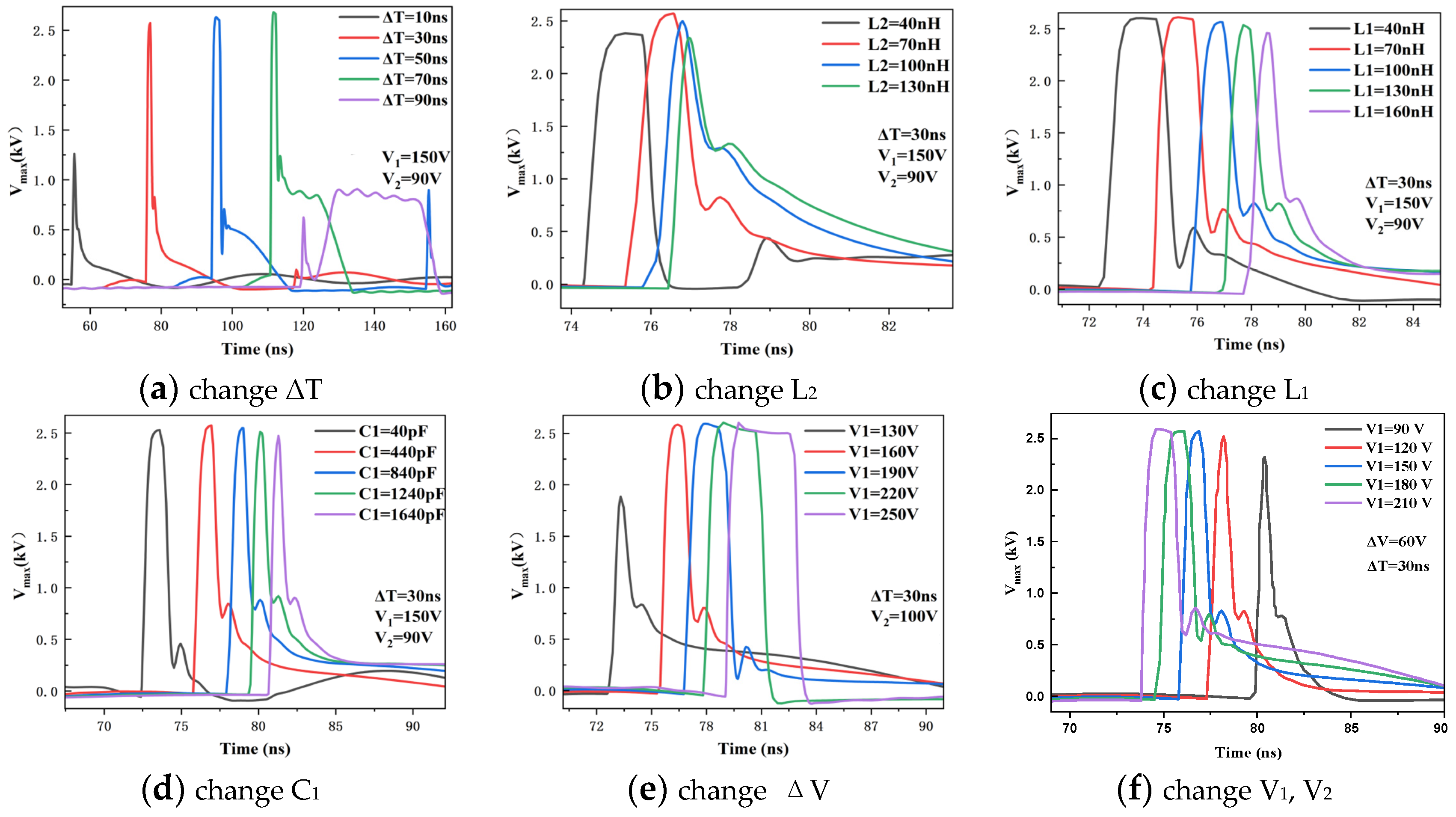
In order to analyze the impact of the parameter changes on the waveform of the output pulse, the simulation based on the software Pspice (https://www.pspice.com/ (accessed on 26 January 2024)) is conducted. Figure 6a shows the simulation output pulse waveform with a different conduction time ΔT, which is changed from 10 ns to 90 ns with an interval of 20 ns. It can be seen that when ΔT = 10 ns, the output pulse is relatively low due to the MOS being turned off at a small current in circuit loop1. When the ΔT changes from 30 ns to 70 ns, the pulse amplitude increases slightly, and the energy of each power pulse also improves. As energy increases, electromagnetic interference becomes more serious, which brings a larger secondary pulse. When ΔT = 90 ns, the output pulse disappears due to the large recombination of carriers in the DSRD base region. Figure 6b shows the simulation output pulse waveform with a different conductor, L2, which is changed from 40 nH to 130 nH with an interval of 30 nH. It can be seen that when L2 = 70 nH, the pulse amplitude reaches its peak value. As the L2 increases, both the pulse delay and pulse discharge time are prolonged. Figure 6c shows the simulation output pulse waveform with a different conductor, L1, which is changed from 40 nH to 160 nH with an interval of 30 nH. It can be seen that a smaller L1 should make the output pulse appear unexpectedly flat-topped, and a larger L1 should make the pulse amplitude reduce. Figure 6d shows the simulation output pulse waveform with a different capacitor C1, which is changed from 40 pF to 1640 pF with an interval of 400 pF. It can be seen that when C1 = 440 pF, the pulse amplitude reaches its highest value. Figure 6e shows the simulation output pulse waveform with a different ΔV by adjusting V1, which is changed from 30 V to 150 V with an interval of 30 V. It can be seen that the pulse amplitude does not change significantly, but the pulse width increases which means the pulse energy is related to the ΔV. Figure 6f shows the simulation output pulse waveform with different V1 and V2 while maintaining a constant ΔT. When V1 increases to 150 V, the pulse amplitude no longer changes. However, considering that the energy storage of the inductor L1 is small when the V1 is low, the pulse amplitude is decreased due to insufficient energy storage. For trade-offs, V1 = 210 V is optimal.
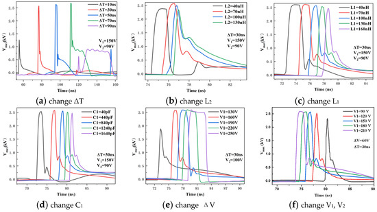
Figure 6.
Changing circuit parameters; the output peak Vmax change curve.
5. Experimental Result
According to the parameters obtained in Table 1, a pulse generator prototype was built based on a self-developed SiC DSRD, as shown in Figure 7a. We selected the IXRFD630 driver from IXYS company and the DE475-102N21A RF MOSFET as a switch. Figure 7b shows that the Tektronix MSO64B Oscilloscope captures the output waveform. The output load uses two 30 dB attenuators connected to the oscilloscope via coaxial lines. The SDN-414-05 current divider from T&M Germany was used to obtain the current flowing through the DSRD.
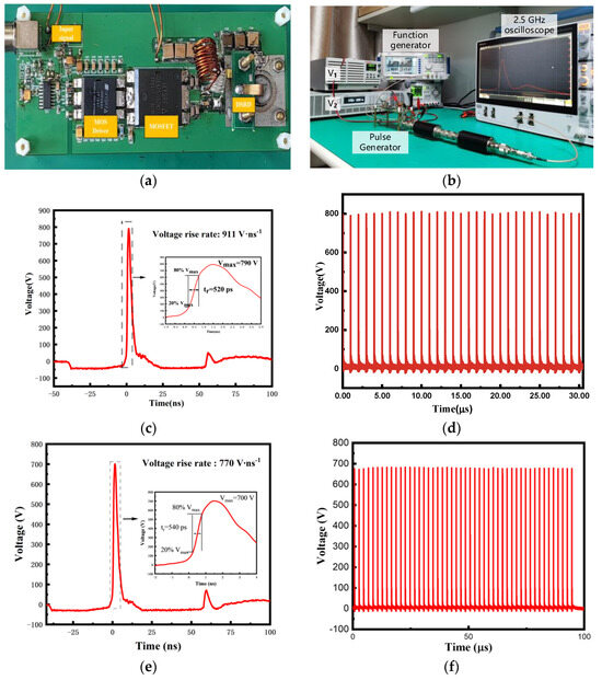
Figure 7.
The pulse generator and output waveforms of the pulse generator are based on SiC DSRD. (a) Pulse generator based on self-developed SiC DSRD; (b) the test platform; (c) output voltage waveform of pulse generator with 790V; (d) output voltage waveform of pulse generator with peak amplitude 790 V and 1 MHz repetition rate under V1 = 120 V, V2 = 40 V; (e) output voltage waveform of pulse generator with peak amplitude 700 V under V1 = 90 V, V2 = 30 V; (f) output voltage waveform of pulse generator with peak amplitude 700 V and 500kHz repetition rate under V1 = 90 V, V2 = 30 V.
Figure 7c shows the waveform of a single power pulse. It can be seen that there is no pre-pulse in the output waveform. The peak voltage is 790 V, and the pulse rise time is 520 ps, which meets the design requirements (820 V) of the pulse generator. In addition, there is a slight secondary pulse observed in the waveform. Figure 7d shows the test result of the pulsed generator with a repetition rate of 1 MHz under V1 = 120 V, V2 = 40 V. Figure 7e,f show the output voltage waveform of the pulse generator with 700 V and 500 kHz repetition rate under V1 = 90 V, V2 = 30 V. The stable output pulse indicates the excellent stability of the pulsed generator.
6. Conclusions
According to the operating principle of DSRDs, this paper presents a collaborative design method of a SiC DSRD and the pulse generator based on it. An optimal method of DSRD parameters is proposed from the viewpoint of driving circuit requirements. In addition, a detailed simulation is conducted to verify design considerations and to analyze the impact of driving parameter changes on the output pulse waveform. A pulse generator based on a SiC DSRD was developed. The experimental results show that the generator can output a peak voltage of 790 V on a matching load of 50 Ω, with a pulse rise time of 520 ps. The pulse front is in the sub-nanosecond level with good stability and can be applied in miniaturized ultra-wideband electromagnetic pulse generators.
Author Contributions
Formal analysis, J.G.; investigation, J.G., Y.Z. (Yu Zhang) and Y.Z. (Yu Zhou); resources, L.S.; data curation, J.G.; writing—original draft preparation, J.G. and Y.C.; writing—review and editing, Y.C.; visualization, Y.C.; supervision, L.S.; project administration, Q.S., X.T. and Y.Z. (Yuming Zhang). All authors have read and agreed to the published version of the manuscript.
Funding
This research was funded by the National Natural Science Foundation of China (Program No. 62174123).
Data Availability Statement
The authors confirm that the data supporting the findings of this study are available within this article.
Acknowledgments
The authors thank all the anonymous reviewers for their very helpful comments in improving the paper.
Conflicts of Interest
The authors declare no conflicts of interest.
References
- Jiang, W.H. Repetition rate pulsed power technology and its applications. High Power Laser Part. Beams 2012, 24, 10–15. [Google Scholar] [CrossRef]
- van Heesch, E.; Pemen, A.; Huijbrechts, P.; van der Laan, P.; Prasinski, K.; Zanstra, G.; de Jong, P. A fast pulsed power source applied to treatment of conducting liquids and air. IEEE Trans. Plasma Sci. 2000, 28, 137–143. [Google Scholar] [CrossRef]
- Lyublinsky, A.G.; Korotkov, S.V.; Aristov, Y.V.; Korotkov, D.A. Pulse power nanosecond-range DSRD-based generators for electric discharge technologies. IEEE Trans. Plasma Sci. 2013, 41, 2625–2629. [Google Scholar] [CrossRef]
- Matsumoto, T.; Wang, D.; Namihira, T.; Katsuki, S.; Akiyama, H. Performances of nanosecond pulsed discharge. Acta Phys. Pol. A 2009, 115, 1101–1103. [Google Scholar] [CrossRef]
- Grekhov, I.V.; Mesyats, G.A. Nanosecond semiconductor diodes for pulsed power switching. Phys.-Uspekhi 2005, 48, 703. [Google Scholar] [CrossRef]
- Efanov, V.M.; Kardo-Sysoev, A.F.; Larionov, M.A.; Tchashnikov, I.G.; Yarin, P.M.; Kriklenko, A.V. Powerful semiconductor 80 kV nanosecond pulser. In Proceedings of the 11th IEEE International Pulsed Power Conference, Baltimore, MD, USA, 29 June–2 July 1997; pp. 985–987. [Google Scholar]
- Kesar, A.S.; Merensky, L.M.; Ogranovich, M.; Kardo-Sysoev, A.F.; Shmilovitz, D. 6-kV, 130-ps rise-time pulsed-power circuit featuring cascaded compression by fast recovery and avalanche diodes. Electron. Lett. 2013, 49, 1539–1540. [Google Scholar] [CrossRef]
- Krasnykh, A. Overview of driver technologies for nanosecond TEM kickers. In Proceedings of the 7th International Particle Accelerator Conference (IPAC 2016), Busan, Republic of Korea, 3 May 2016; pp. 3645–3647. [Google Scholar]
- Benwell, A.; Burkhart, C.; Krasnykh, A.; Tang, T.; Kardo-Sysoev, A. A 5 kV, 3 MHz solid-state modulator based on the DSRD switch for an ultra-fast beam kicker. In Proceedings of the IEEE International Power Modulator and High Voltage Conference (IPMHVC), San Diego, CA, USA, 23 May 2013; pp. 328–331. [Google Scholar]
- Fang, X.; Ding, Z.; Hao, Q.; Yuan, X.; Hu, L.; Fan, Y. Study on generation of drift step recovery diodes for sub-nanosecond switching and high repetition rate operation. In Proceedings of the 4th China Pulsed Power Conference, Hohhot, China, 25 August 2015; pp. 351–354. [Google Scholar]
- Ilyin, V.A.; Afanasyev, A.V.; Ivanov, B.V.; Kardo-Sysoev, A.F.; Luchinin, V.V.; Reshanov, S.A. High-voltage ultra-fast pulse diode stack based on 4H-SiC. Mater. Sci. Forum 2016, 858, 786–789. [Google Scholar] [CrossRef]
- Ivanov, B.V.; Smirnov, A.A.; Shevchenko, S.A.; Afanasyev, A.V.; Ilyin, V.A. High voltage sub-nanosecond silicon carbide opening switch. In Proceedings of the 57th International Scientific Conference on Power and Electrical Engineering of Riga Technical University (RTUCON), Riga, Latvia, 13–14 October 2016; pp. 1–4. [Google Scholar]
- Goto, T.; Shirai, T.; Tokuchi, A.; Naito, T.; Fukuda, K.; Iwamuro, N. Experimental demonstration on ultra-high voltage and high speed 4H-SiC DSRD with smaller numbers of die stacks for pulse power. Mater. Sci. Forum 2018, 924, 858–861. [Google Scholar] [CrossRef]
- Ilyin, V.A.; Afanasyev, A.V.; Demin, Y.S.; Ivanov, B.V.; Kardo-Sysoev, A.F.; Luchinin, V.V. 30 kV pulse diode stack based on 4H-SiC. Mater. Sci. Forum 2018, 924, 841–844. [Google Scholar] [CrossRef]
- Wang, Y.; He, P.; Jing, X.; Tie, W.; Xie, J.; Zhao, C. Simulation and calculation of pulsed power source based on drift step recovery diode switching. High Power Laser Part. Beams 2018, 30, 095005. [Google Scholar]
- Sun, R.; Zhang, K.; Chen, W.; Xia, Y.; Tan, J.; Chen, Y. 10-kV 4H-SiC Drift Step Recovery Diodes (DSRDs) for Compact High-repetition Rate Nanosecond HV Pulse Generator. In Proceedings of the 32nd International Symposium on Power Semiconductor Devices and ICs (ISPSD), Vienna, Austria, 18 August 2020; pp. 62–65. [Google Scholar]
- Yang, Z.W.; Liang, L.; Yan, X.X. Dynamic Electrical Characteristics of 4H-SiC Drift Step Recovery Diodes of High Voltage. IEEE Trans. Plasma Sci. 2022, 50, 1276–1281. [Google Scholar] [CrossRef]
- Kyuregyan, A.S. Theory of Drift Step Recovery Diodes. Solid State Electron. 2004, 49, 720–727. [Google Scholar] [CrossRef]
- Ivanov, B.V.; Smirnov, A.A.; Shevchenko, S.A. A Study of Charge Losses in 4H-SiC Drift Step Recovery Diodes (DSRD). In Proceedings of the of EIConRusNW, St. Petersburg, Russia, 3 February 2016; pp. 51–52. [Google Scholar]
- Ivanov, P.A.; Konkov, O.I.; Samsonova, T.P.; Potapov, A.S.; Grekhov, I.V. Dynamic Characteristics of 4H-SiC Drift Step Recovery Diodes. Semiconductors 2015, 49, 1511–1515. [Google Scholar] [CrossRef]
- Galeckas, A.; Linnros, J. Investigation of surface recombination and carrier lifetime in 4H/6H-SiC. Mater. Sci. Eng. 1999, 61, 239–243. [Google Scholar] [CrossRef]

Disclaimer/Publisher’s Note: The statements, opinions and data contained in all publications are solely those of the individual author(s) and contributor(s) and not of MDPI and/or the editor(s). MDPI and/or the editor(s) disclaim responsibility for any injury to people or property resulting from any ideas, methods, instructions or products referred to in the content. |
© 2024 by the authors. Licensee MDPI, Basel, Switzerland. This article is an open access article distributed under the terms and conditions of the Creative Commons Attribution (CC BY) license (https://creativecommons.org/licenses/by/4.0/).