Article

Design of a Switching Strategy for Output Voltage Tracking Control in a DC-DC Buck Power Converter

by
Eduardo Hernández-Márquez
1,*,
Panuncio Cruz-Francisco
2,*,
Eric Hernández-Castillo
2,
Dulce Martinez-Peón
3,
Rafael Castro-Linares
4,
José Rafael García-Sánchez
5,
Alfredo Roldán-Caballero
6,
Xóchitl Siordia-Vásquez
7 and
Juan Carlos Valdivia-Corona
8
1
Departamento de Mecatrónica, Instituto Tecnológico Superior de Poza Rica, Tecnológico Nacional de México, Veracruz 93230, Mexico
2
División de Estudios de Posgrado y de Investigación, Tecnológico de Tlalnepantla, Tecnológico Nacional de México, Estado de México 54070, Mexico
3
Departamento de Ingeniería Eléctrica y Electrónica, Instituto Tecnológico de Nuevo León, Tecnológico Nacional de México, Nuevo León 67170, Mexico
4
Departamento de Ingeniería Eléctrica, Centro de Investigación y Estudios Avanzados del Instituto Politécnico Nacional, Ciudad de México 07360, Mexico
5
División de Ingeniería Mecatrónica, Tecnológico de Estudios Superiores de Huixquilucan, Tecnológico Nacional de México, Estado de México 52773, Mexico
6
Unidad Profesional Interdisciplinaria de Ingeniería Campus Tlaxcala, Instituto Politécnico Nacional, Tlaxcala 90000, Mexico
7
Facultad de Ingeniería en Electrónica y Comunicaciones, Universidad Veracruzana, Veracruz 93390, Mexico
8
División de Ingeniería en Sistemas Automotrices, Tecnológico de Estudios Superiores del Oriente del Estado de México, Tecnológico Nacional de México, Estado de México 56400, Mexico
*
Authors to whom correspondence should be addressed.
Electronics 2024, 13(12), 2252; https://doi.org/10.3390/electronics13122252
Submission received: 13 May 2024 / Revised: 3 June 2024 / Accepted: 5 June 2024 / Published: 8 June 2024
(This article belongs to the Special Issue Applications, Control and Design of Power Electronics Converters)

Abstract

:
This work proposes the design of a commutation function to solve the output voltage trajectory tracking problem in the DC-DC Buck power electronic converter. Through a Lyapunov-type analysis, sufficient conditions are established, taking into account the discontinuous model, to ensure asymptotic convergence to the desired trajectories. Based on this analysis, a state-dependent switching function was designed to guarantee the closed-loop stability of the tracking error. To validate the control performance, circuit numerical simulations were carried out under abrupt disturbances in the source and load of the converter. The results demonstrate that the voltage tracking at the output of the converter is satisfactorily achieved.

1. Introduction

DC-DC power electronic converters are circuits controlled by opening or closing one or two switches, depending on the circuit configuration, using the output voltage and other state variables to carry out voltage control [1]. This type of circuit is mainly used to improve efficiency in applications where voltage control is realized accurately, avoiding unwanted effects that occur with pulse width modulation (PWM) controllers. PWM control generates an undesirable dynamic effect on its output, generally as a result of a noisy output signal, as well as current spikes, elements that are not favorable for either the power supply or the circuit load such as another circuit or an application [2,3,4,5,6,7,8]. In the particular case of the Buck-type converter, there are two elements that can store energy, a coil and a capacitor, which reduces the amplitude of the effects generated by the commutation of the switches of the circuit, on the output signal [2].
The Buck power converter is controlled using some linear classical control techniques like proportional integral control [9,10]. However, they have disadvantages such as noise sensitivity or reduced robustness [11]. The Buck converter can be studied under the hybrid system scheme; in this case, a control strategy commutates between the sub-systems that describe the dynamics of the converter, ensuring stabilization or monitoring tasks. Daaecto et al., in [12], designed a control for switched systems, specifically to deal with switched converters like Buck converters, where the main goal is the determination of a switching function that ensures global stability for a range of values in the load voltage. Later, Júnior et al., in [13], presented a design utilizing a single quadratic Lyapunov function for the expedited convergence of DC–DC converters within a class of switched systems for voltage regulation. A robust state-feedback switching law for the switched system utilizing the sliding mode theory was developed in [14] to ensure the robust asymptotic stability of the desired equilibrium point for the Buck converter. While Hejri, in [15], using switched Lyapunov functions, a set of sufficient conditions based on matrix inequalities, reduced the computational complexity and solved the stabilization problem for the DC/DC converter, de Souza et al. in [16] developed a strategy to limit the switching frequency using a state-dependent switching law for switched systems for stabilization at the desired equilibrium. Another switching strategy consists of an adaptive sliding mode control that combines a robust proportional-derivative control law for the regulation of the DC/DC Buck converter–DC motor system presented in [17]. Additionally, Júnior et al., in [18], introduced a control based on Lyapunov stability using a quadratic function and linear matrix inequalities to improve the convergence speed to a constant reference voltage in the Buck DC-DC power converter. Recently, Hashemi et al., in [19], proposed a controller leveraging the power of composite switched Lyapunov functions to ensure stability for linear-switched systems, such as the Buck converter, with constant external input.
Motivated by the benefits of a commutated control strategy [12,13,14,15,16,17,18,19], the design of a suitable switching function by means of the application of convex sets for the output trajectory tracking of a Buck power electronic converter is presented here. Unlike in [12,13,14,15,16,17,18,19], this control resolves voltage tracking at the converter load. The use of convex sets in the commutated control strategy presented here allows for resolving the tracking for different desired voltage trajectories for the Buck converter in milliseconds, even in the presence of abrupt disturbances in the load and source. Additionally, this design represents an advantage over classical control methods that require PWM combined with modulation stage methods such as [20] and studies that simply consider the averaged model [21] in terms of the ability to reduce the complexity of control implementation in the system.
The rest of this document is organized as follows. Section 2 describes the problem statement with the control objective of this work. Section 3 defines the mathematical background needed to develop the control strategy. Section 4 states the main result summarized in a main theorem. Afterward, numerical and circuit simulations of the designed controller are presented in Section 5. Finally, in Section 6, the work concludes by providing some important remarks.

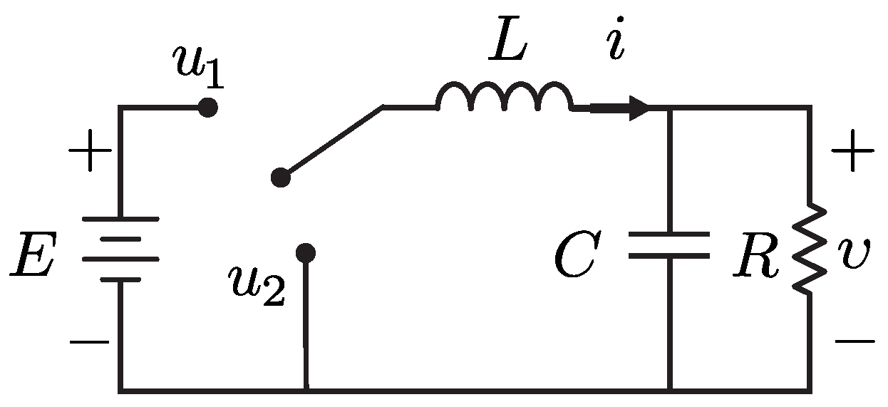
2. Problem Statement

The class of switching systems to study is described by the following set of linear differential equations:
x ˙ = A σ x + B σ U c , y = C σ x ,
where x R n is the state vector, U c R m is a constant input signal for all t 0 , and y R p is the set of variables (or output) used to control the system. The switching signal defined as σ : t I selects an element of the index set I = { 1 , 2 , , N } , such that for each instant of time t 0 , the function value corresponds to an index of one of the N available sub-systems. The i esim sub-system is composed of the set of matrices A i R n × n , B i R n × m , and C i R p × n that define the system (1); in other words,
G i = A i B i C i 0 , i I .
A particular case of the commuted systems described by Equation (1) corresponds to the DC-DC Buck power electronic converter, which is presented in Figure 1.
The Buck converter can be seen as two different circuits, also called operating modes, with each one working on some time intervals given by a switch; see Figure 2. Thus, when the switch position is in u 1 , the power supply provides energy to the system, charging the inductor L and the capacitor C. In this case. the voltage, υ , in the load R grows until a given voltage level is reached. Alternatively, when the switch position is in u 2 , the inductor and the capacitor are discharged through R. The commutation of the transistor Q plus the diode D allows a control in the voltage of the terminals of R.
For this particular case, I = { 1 , 2 } . The state vector x = i υ T takes the values of the current in L and voltage in R. The switching function σ allows the selection between two different systems composed of the set G i , where each matrix is defined as
A 1 = A 2 = 0 1 L 1 C 1 R C , B 1 = E L 0 , B 2 = 0 0 , C 1 = C 2 = 0 1 .
The objective of this work was to design a switching strategy σ such that the tracking error defined by
e : = y y d
converges asymptotically to the origin. In (4), y d R is a given a differentiable reference signal r 1 times for the controlled output y. And y d , y ˙ d , and y ¨ d are bounded by some constants y d ( j ) y ¯ d ( j ) R + for j = 0 , 2 ¯ .

3. Mathematical Concepts

Here, three mathematical concepts are defined to be used in the development of the main result in this manuscript. The more explanation about the symbols can be found in Appendix A.
Definition 1 
(Convex set). A set A R n is said to be convex if λ x + ( 1 λ ) y A for all x A , y A , and λ [ 0 , 1 ] . The intersection of n different convex sets is a convex set, and if A R n and B R n are convex and α and β are real numbers, then the set α A + β B is convex [22].
Definition 2 
(Convex hull). Let A R n . The intersection of all the convex sets contained in A is called the convex hull of A , and it is defined as c o A [22]. The convex hull can be represented by the vector sum
λ 1 x 1 + + λ m x m ,
which corresponds to the convex combination of x 1 , , x m if λ i 0 , i = 1 , m ¯ , and λ 1 + + λ m = 1 . If x 1 , , x m are vectors of A , then any combination of x 1 , , x m belongs to c o A .
Definition 3 
(Relative degree [23]). Consider the following linear system:
x ˙ = A x + B u , y = C x ,
with A , B and C being matrices with appropriate dimensions. System (5) is said to have relative degree r if
C A k B = 0 , C A r 1 B 0 , 0 k < r 1 .

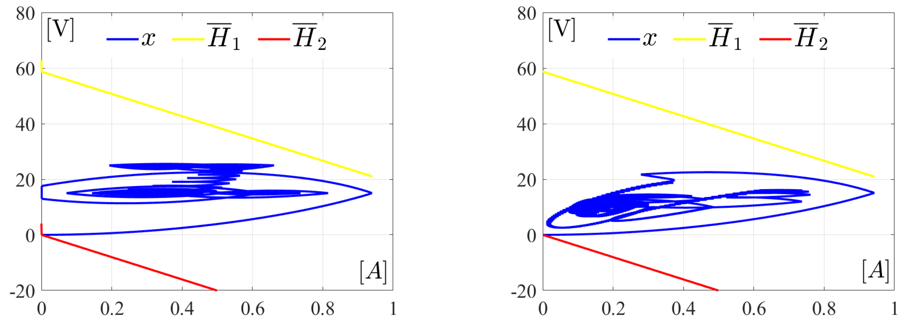
4. Stabilizing Switching Signal Design

Before introducing the main result of this work, it is necessary to find the error dynamics by derivating Equation (4). This yields
e ˙ = y ˙ y ˙ d = C σ x ˙ y ˙ d = C σ A σ x + C σ B σ U c y ˙ d ,
In noting that C σ B σ U c = 0 for any value of σ (see (3)), the second derivative of the tracking error is calculated:
e ¨ = C σ A σ x ˙ y ¨ d = C σ A σ A σ x + B σ U c y ¨ d = C σ A σ 2 x + C σ A σ B σ U c y ¨ d ,
For this case, it is clear that C σ A σ B σ U c 0 for σ = 1 , and C σ A σ B σ U c = 0 for σ = 2 . From the definition of the relative degree, it can be stated that r = 2 for σ = 1 .
Selecting as states variables e 1 = e and e 2 = e ˙ , one obtains
e ˙ 1 = e 2 ,
e ˙ 2 = e ¨ = C σ A σ 2 x + C σ A σ B σ U c y ¨ d .
In defining U σ : = C σ A σ 2 x + C σ A σ B σ U c , notice that on any given time interval T = [ t 1 , t 2 ] , t 2 > t 1 , it is possible to generate an average value u a v for U σ between two constant inputs U 1 and U 2 using an adequate switching function σ , a sufficient condition for the existence of this switching function [24] is that u a v c o { U 1 , U 2 } . Additionally, the state space representation can be rewritten as
e ˙ = A ˜ e + B ˜ U σ y ¨ d ,
where A ˜ = 0 1 0 0 , and B ˜ = 0 1 . In order to analyze the conditions on σ to achieve stability for the tracking error, consider the following Lyapunov candidate function:
V ( e ) = e T P e ,
with P = P T > 0 and its derivate given by
V ˙ ( e , σ ) = 2 e T P e ˙ = 2 e T P A ˜ e + B ˜ U σ y ¨ d .
Lemma 1. 
For a given positive definite Q = Q T > 0 and some given positive scalars K 1 and K 2 , consider the Lyapunov candidate function (12) and its derivate described by (13), with the matrix P satisfying
P A e + A e T P = Q ,
for the matrix
A e = 0 1 K 1 K 2 .
Then, the tracking error (4) converges asymptotically to the origin if there exists a switching function σ that generates an average equivalent input:
u a v = y ¨ d K 1 y K 2 y ˙ + K 1 y d + K 2 y ˙ d .
Proof. 
By (16),
U σ ( x ) = u a v = K 1 e 1 K 2 e 2 + y ¨ d ,
In substituting this expression in (13) and by (14),
V ˙ ( e ) = e T P A e + A e T P e = e T Q e < 0
So, the tracking error converges asymptotically to the origin. □
Let us define the following matrices:
H : = C i A i 2 + K 1 C i + K 2 C i A i , S i : = C i A i B i + K 2 C i B i .
Now, the following Theorem presents conditions on the existence of σ such that U σ ( x ) = u a v and a possible manner to generate this as a function of the tracking error, i.e., σ = σ ( e ) .
Theorem 1. 
Consider system (1); with the tracking error dynamics given in (9) and with the candidate Lyapunov function (12), if there exists x R n such that
j = 1 2 K j d j y d d t j c o H x + S i U c , for all t 0 ,
then U σ = u a v for
σ ( e ) = arg min i I e T P B ˜ U i y ¨ d ,
and u a v , P, K 1 , and K 2 are as given in Lemma 1.
Proof. 
In adding and subtracting j = 1 2 K j d j y d d t j to e ˙ 2 in (9) and substituting in the derivative of V for a fixed σ = i ,
V ˙ ( e , i ) = e T Q e + 2 e T P B ˜ C i A i 2 x + C i A i B i U c + K 1 e 1 + K 2 e 2 y ¨ d
From the definitions of e 1 and e 2 and condition (14),
V ˙ ( e , i ) 2 e T P B ˜ H x + S i U c j = 1 2 K j d j y d d t j .
Condition (18) implies that there always exists i I such that
e T P B ˜ H x + S i U c j = 1 2 K j d j y d d t j < 0 ,
for each t 0 , this ensures that V ˙ ( e , i ) < 0 for some i I . Finally, from the definition U i = C i A i 2 x + C i A i B i U c ,
U i y ¨ d = H x + S i U c j = 1 2 K j d j y d d t j ,
this implies that (19) selects the corresponding index for each e in any time instant t 0 . □
Condition (18) asks for the existence of an x belonging to the convex set defined by the half-planes characterized by H and S i U c for the scalars K 1 and K 2 and the function y d such that j = 1 2 K j d j y d d t j for each instant t 0 . However, it is much easier to verify the following sufficient condition:
j = 1 2 K j d j y d d t j c o { H x + S i U c } ,
This condition only depends on x; all the other variables can be calculated a priori, and for gain design purposes, it is only required that for the selected K 1 and K 2 , the set c o { H x + S i U c } .

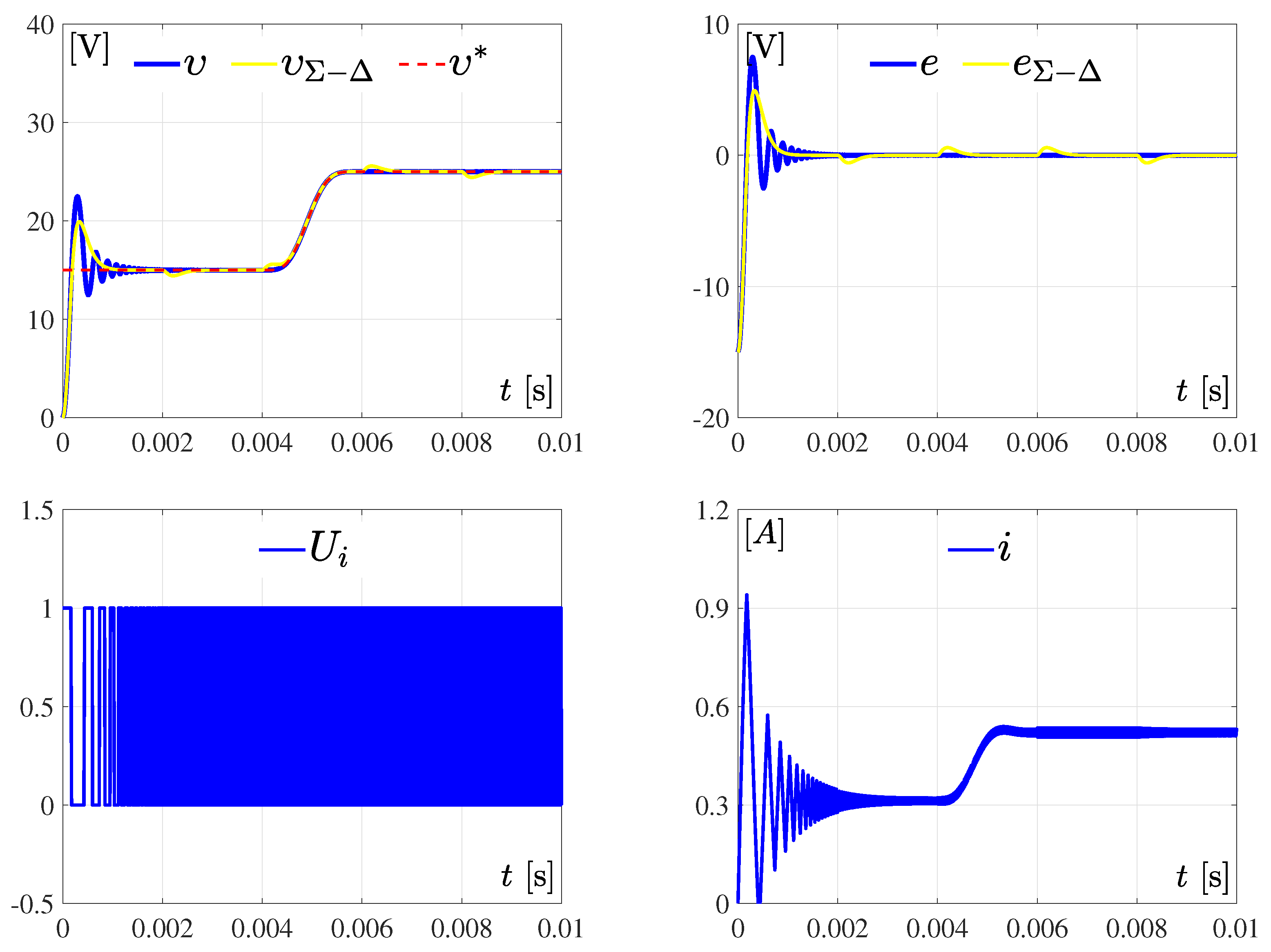
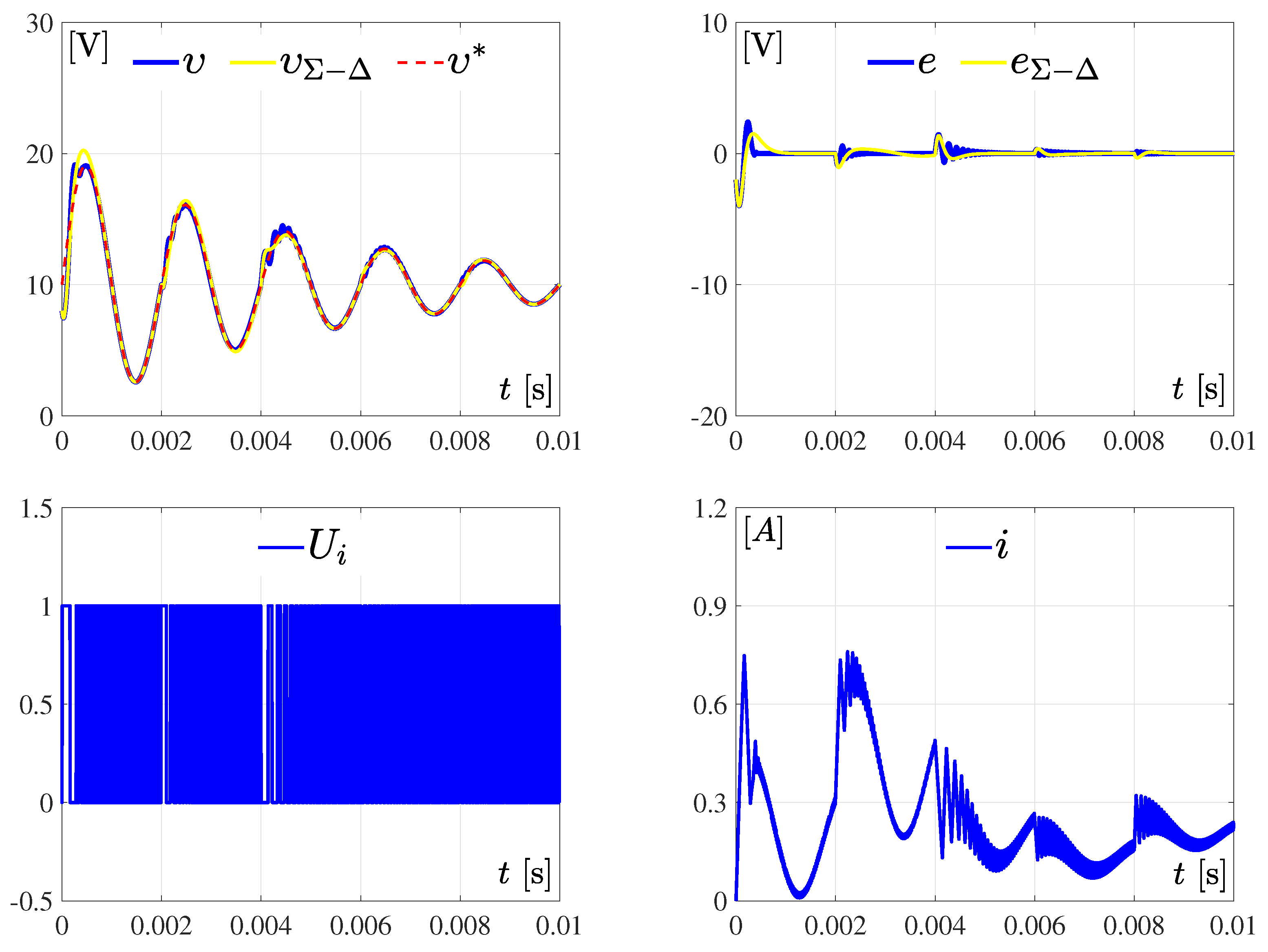
5. Simulation Results

With the aim of enhancing the contribution of this work, control (21) was compared with a control based on differential flatness and the Σ Δ modulator [25]. Thus, this section presents the simulation results of the aforementioned controllers.

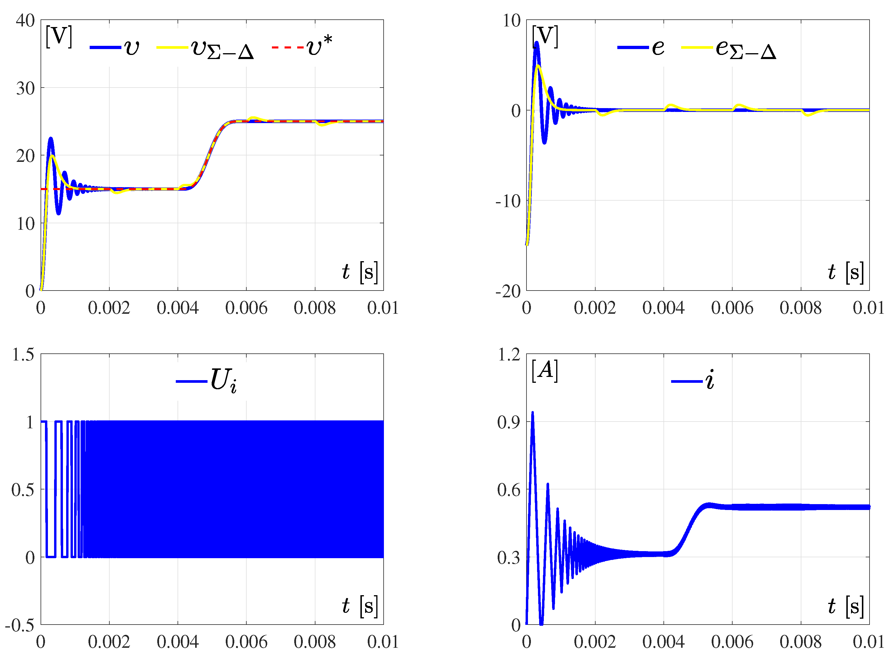
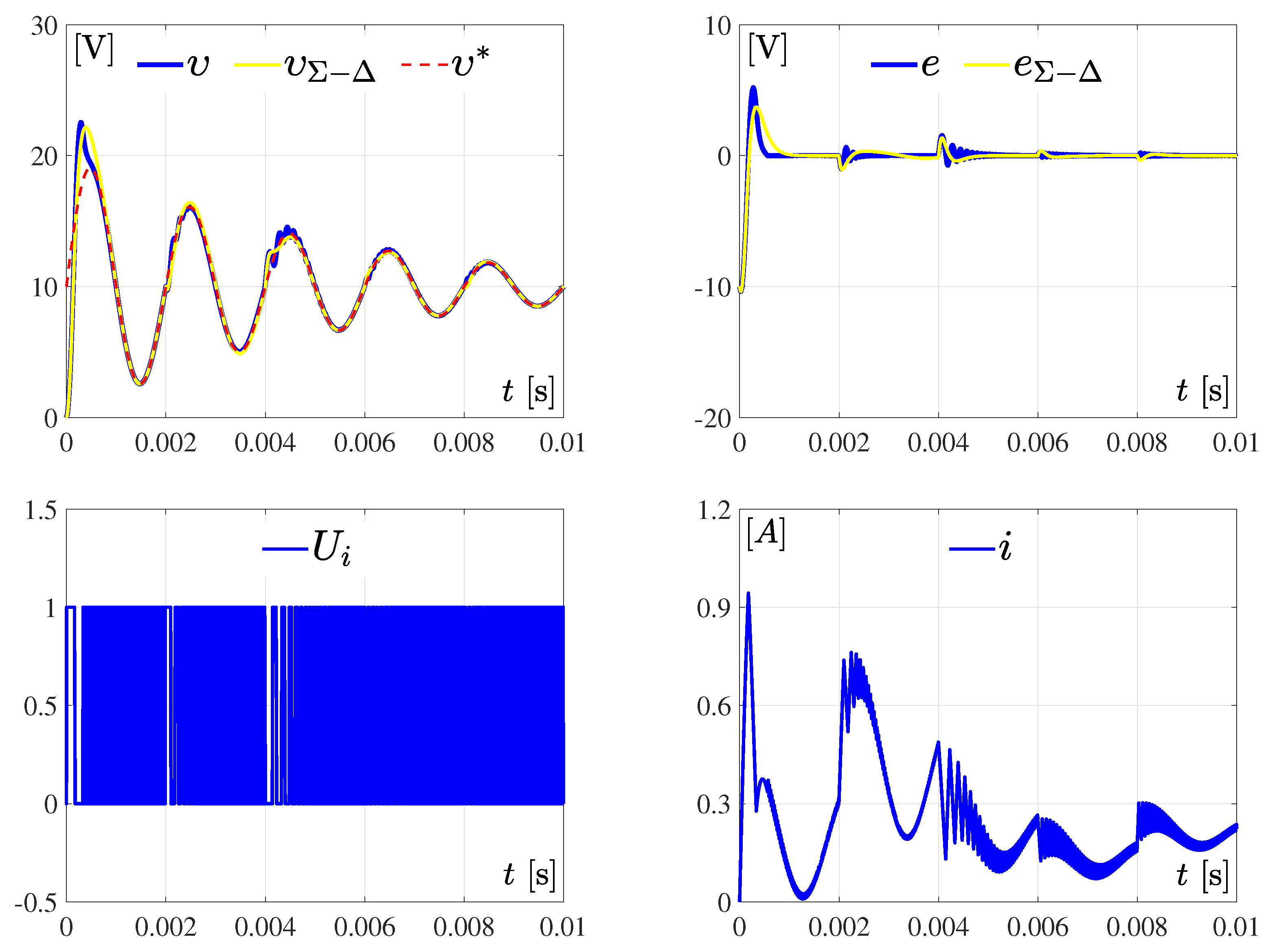
5.1. Switching Function Control

The control proposed in this work is summarized as follows: in declaring y d = υ * , with υ * being the desired voltage, Equation (21) can be expressed in a more convenient form as follows:
U i = υ ¨ * + H x + S i U c j = 1 2 K j d j υ * d t j ,
with ( K 1 , K 2 ) > 0 and
H : = C i A i 2 + K 1 C i + K 2 C i A i , S i : = C i A i B i + K 2 C i B i .
for some i 1 , 2 .

5.2. Differential Flatness Control and Σ Δ Modulator

In the design of this control, the property of differential flatness of the Buck converter was exploited. The control law that enables voltage tracking at the converter output through differential flatness was reported in [25] and is composed as follows:
u a v = L C E μ + L R E υ ˙ + 1 E υ ,
with
μ = υ ¨ * β 2 υ ˙ υ ˙ * β 1 υ υ * β 0 0 t υ υ * d τ ,
where
β 2 = a + 2 ξ ω n , β 1 = 2 ξ ω n a + ω n 2 , β 0 = a ω n 2 ,
given a > 0 , ξ > 0 , and ω n > 0 coefficients of a Hurwitz polynomial and a u a v average input control. The implementation of control (25) in the Buck converter is carried out through the Σ Δ modulator, as shown in Figure 3.

5.3. Parameters for the Numerical Simulations

The mathematical model of the DC/DC Buck converter is described as follows [25]:
x ˙ = 0 1 L 1 C 1 R C x + E L 0 U i , y = 0 1 x ,
with x = i υ T . The Buck converter parameter values that will be used in the simulations are the following:
R = 48   Ω , L = 4.94 mH , C = 4.7 μ F , E = 32 V .
These values are selected in such a way as to obtain moderate current and voltage ripples [26] and, additionally, to satisfy condition (18). The proposed trajectories for voltage monitoring at the output of the Buck converter are two: one a Bézier type (29) and the other a sinusoidal type with exponential amplitude (30). It is important to consider that such trajectories respect the dynamics of the converter, i.e., υ * E .
  • Bézier-type trajectory 
υ * = υ ¯ i + υ ¯ f υ ¯ i φ t , t i , t f ,
with υ ¯ i = 15 V , υ ¯ f = 25 V , and φ t , t i , t f given by
φ t , t i , t f = 0 for t t i , t t i t f t i 5 252 1050 t t i t f t i + 1800 t t i t f t i 2   1575 t t i t f t i 3 + 700 t t i t f t i 4 126 t t i t f t i 5   for t ( t i , t f ) , 1 for t t f ,
where [ t i , t f ] = [ 0.004 s , 0.006 s ] .
  • Sinusoidal trajectory 
υ * = 10 + 10 e 200 t sin 1000 π t .
Regarding the control gains via switching function (23), they were selected according to (18) and are the following:
K 1 = 10 , K 2 = 10 .
The graphs shown in Figure 4 present how state x remains within the boundaries H ¯ 1 and H ¯ 2 obtained from (18) for the trajectories (29) and (30), respectively. Therefore, it will be satisfactorily followed by the control designed here; on the other hand, if the state has parts outside the boundary, it cannot be assured that the tracking problem will be solved correctly.
Substituting the gains K 1 and K 2 into (24) produces
h 11 = 940.98 × 10 6 , h 21 = 23.47 × 10 6 , S 1 = 1.3782 × 10 9 , S 2 = 0 .
where h 11 and h 21 are elements of H (24).
Regarding the control gains (27), the values considered are a = 10,000, ξ = 1 , and ω n = 10,000.
In order to highlight the robustness of the control, abrupt disturbances in the voltage source and load defined in (31) and (32), respectively, are considered.
  • Disturbance in voltage source 
E p = E 0 t < 0.002 s , 75 % E 0.002 t < 0.004 s , E 0.004 t < 0.006 s , 125 % E 0.006 t < 0.008 s , E 0.008 t s .
  • Load disturbance 
R p = R 0 t < 0.002 s , 50 % R 0.002 t < 0.004 s , R 0.004 t < 0.006 s , 150 % R 0.006 t < 0.008 s , R 0.008 t s .

5.4. Numerical Simulations

The numerical simulations of the switched controllers were carried out via MATLAB-Simulink, using the Euler numerical method with a fixed step size of 0.0000001. The results shown in Figure 5, Figure 6, Figure 7 and Figure 8 use the following nomenclature: υ , e, U i , and i represent the voltage, voltage tracking error (4), and current for the Buck converter with control via switching function (23), respectively, whereas υ Σ Δ and e Σ Δ are the voltage and voltage tracking error for control (25), respectively. Finally, υ * is the desired voltage.

5.5. Simulations with Circuits

The simulations of the switched control in the Buck converter were carried out via SimPowerSystems in MATLAB-Simulink using the Euler numerical method with a fixed step size of 0.0000001 (Figure 9), and the converter operated in continuous conduction mode. The results shown in Figure 10, Figure 11, Figure 12 and Figure 13 use the same nomenclature as that used in Section 5.4.

5.6. Comments

From Figure 5, Figure 6, Figure 7, Figure 8, Figure 9, Figure 10, Figure 11, Figure 12 and Figure 13, it can be seen that in both simulations, it is possible to solve the voltage tracking almost immediately, even in the presence of abrupt disturbances in the source and the load for both controls. However, differential flatness control (25) requires high gains to achieve good tracking. This can be counterproductive, as it can increase energy consumption, on one hand, and amplify noise in the input signal due to the derivative component of the control, on the other. In addition to the comparative error tracking graphs, it is observed that control (23) generally solves the tracking task faster than control (25). On the other hand, it can be seen how the control (23) is capable of compensating for load variations through the current that circulates in the circuit, keeping the current within a moderate range. Due to the desired voltage being non-zero at its onset and due to abrupt changes in the power source and load, the current undergoes transient oscillations before stabilizing.
The only inconvenience that the proposed control here may face is that the desired trajectories must satisfy condition (18) to ensure trajectory tracking. However, a good selection of values for the converter parameters and control gains can overcome the problem.

6. Conclusions

The voltage monitoring at the output of the DC/DC Buck-type power electronic converter through a switching function control was presented here. The desired trajectories were tracked by means of a correct switching function based on the dynamics of the Lyapunov function. In order to observe the control performance, numerical simulations were carried out using a converter circuit in Matlab-Simulink, taking into account abrupt disturbances in the source and load. The simulation results show that the tracking of the converter output voltage is achieved almost immediately.
A crucial aspect of the switching control presented here is that it resolves the tracking of different desired voltage trajectories for the Buck converter using convex sets. This differs from what is presented in state-of-the-art converters, which only focus on bringing the voltage to a desired equilibrium point. This significant improvement is an attractive option for application to commutated systems.
Motivated by the obtained results, future work should aim to build a prototype of the DC/DC Buck converter to experimentally implement the control developed here, potentially adding a current limiter to protect components.

Author Contributions

Conceptualization, E.H.-M., P.C.-F. and E.H.-C.; methodology, E.H.-M., P.C.-F. and E.H.-C.; validation, E.H.-M., R.C.-L., J.R.G.-S. and A.R.-C.; formal analysis, E.H.-M., P.C.-F. and E.H.-C.; investigation, E.H.-M., P.C.-F. and E.H.-C.; resources, E.H.-M., P.C.-F., E.H.-C., D.M.-P., R.C.-L., J.R.G.-S., A.R.-C. and X.S.-V.; data curation, X.S.-V.; writing—original draft preparation, E.H.-M., P.C.-F. and E.H.-C.; writing—review and editing, E.H.-M., P.C.-F. and E.H.-C.; visualization, D.M.-P. and X.S.-V.; supervision, E.H.-M., P.C.-F. and E.H.-C.; project administration, E.H.-M., P.C.-F., E.H.-C., D.M.-P. and X.S.-V.; funding acquisition, E.H.-M., P.C.-F., E.H.-C., D.M.-P., R.C.-L., J.R.G.-S., A.R.-C., X.S.-V. and J.C.V.-C. All authors have read and agreed to the published version of the manuscript.

Funding

This research received no external funding.

Institutional Review Board Statement

Not applicable.

Informed Consent Statement

Not applicable.

Data Availability Statement

Data are contained within the article.

Acknowledgments

The Work of Eduardo Hernández-Márquez, Panuncio Cruz-Francisco, Rafael Castro-Linares, José Rafael García-Sánchez, and Alfredo Roldán-Caballero was supported by CONACYT-México.

Conflicts of Interest

The authors declare no conflicts of interest.

Appendix A

R represents the set of real numbers. j = 1 , m ¯ symbolizes the set containing all integers within the range from 1 to m. The superscript T denotes matrix transposition. The notation Q > 0 signifies that Q is a real-symmetric positively definite matrix. co A denotes the convex hull of A , and arg min x f ( x ) is the set of all values of x for which f ( x ) attains its minimum value.

References

  1. Ling, R.; Maksimovic, D.; Leyva, R. Second-order sliding-mode controlled synchronous Buck DC–DC converter. IEEE Trans. Power Electron. 2016, 31, 2539–2549. [Google Scholar] [CrossRef]
  2. Silva-Ortigoza, R.; Hernández-Guzmán, V.M.; Antonio-Cruz, M.; Muñoz-Carrillo, D. DC/DC Buck power converter as a smooth starter for a DC motor based on a hierarchical control. IEEE Trans. Power Electron. 2015, 30, 1076–1084. [Google Scholar] [CrossRef]
  3. Hernández-Márquez, E.; García-Sánchez, J.R.; Silva-Ortigoza, R.; Antonio-Cruz, M.; Hernández-Guzmán, V.M.; Taud, H.; Marcelino-Aranda, M. Bidirectional tracking robust controls for a DC/DC Buck converter-DC motor system. Complexity 2018, 2018, 1260743. [Google Scholar] [CrossRef]
  4. Zhou, K.; Wu, Y.; Wu, X.; Sun, Y.; Teng, D.; Liu, Y. Research and development review of power converter topologies and control technology for electric vehicle fast-charging systems. Electronics 2023, 12, 1581. [Google Scholar] [CrossRef]
  5. Yang, Z.; Wang, C.; Han, J.; Yang, F.; Shen, Y.; Min, H.; Hu, W. Analysis of voltage control strategies for DC microgrid with multiple types of energy storage systems. Electronics 2023, 12, 1661. [Google Scholar] [CrossRef]
  6. Narayanaswamy, J.; Mandava, S. Non-isolated multiport converter for renewable energy sources: A comprehensive review. Energies 2023, 16, 1834. [Google Scholar] [CrossRef]
  7. Venugopal, R.; Chandrasekar, B.; Savio, A.D.; Narayanamoorthi, R.; Aboras, K.M.; Kotb, H.; Ghadi, Y.Y.; Shouran, M.; Elgamli, E. Review on unidirectional non-isolated high gain DC–DC converters for EV sustainable DC fast charging applications. IEEE Access 2023, 11, 78299–78338. [Google Scholar] [CrossRef]
  8. Coutinho, H.V.; Toledo, J.A.; Silva, L.A.R.; Maia, T.A.C. Design and implementation of a low-cost and low-power converter to drive a single-phase motor. Machines 2023, 11, 673. [Google Scholar] [CrossRef]
  9. Moreno-Valenzuela, J. A class of proportional-integral with anti-windup controllers for DC–DC Buck power converters with saturating input. IEEE Trans. Circuits Syst. II Express Briefs 2020, 67, 157–161. [Google Scholar] [CrossRef]
  10. Aguilar-Ibanez, C.; Moreno-Valenzuela, J.; García-Alarcón, O.; Martinez-Lopez, M.; Acosta, J.A.; Suarez-Castanon, M.S. PI-type controllers and Σ-Δ modulation for saturated DC-DC Buck power converters. IEEE Access 2021, 9, 20346–20357. [Google Scholar] [CrossRef]
  11. Ma, L.; Zhang, Y.; Yang, X.; Ding, S.; Dong, L. Quasi-continuous second-order sliding mode control of Buck converter. IEEE Access 2018, 6, 17859–17867. [Google Scholar] [CrossRef]
  12. Deaecto, G.C.; Geromel, J.C.; Garcia, F.S.; Pomilio, J.A. Switched affine systems control design with application to DC–DC converters. IET Control Theory Appl. 2010, 4, 1201–1210. [Google Scholar] [CrossRef]
  13. Júnior, E.M.; Teixeira, M.C.M.; Cardim, R.; Moreira, M.R.; Assunção, E.; Yoshimura, V.L. On Control design of switched affine systems with application to DC-DC converters. In Frontiers in Advanced Control Systems; de Oliveira Serra, G.L., Ed.; Intech: London, UK, 2012. [Google Scholar]
  14. Noori, A.; Farsi, M.; Mahboobi Esfanjani, R. Design and implementation of a robust switching strategy for DC–DC converters. IET Power Electron. 2016, 9, 316–322. [Google Scholar] [CrossRef]
  15. Hejri, M. Practical stability analysis and switching controller synthesis for discrete-time switched affine systems via linear matrix inequalities. Sci. Iran. 2022, 29, 1–28. [Google Scholar] [CrossRef]
  16. de Souza, R.P.C.; Kader, Z.; Caux, S. Switched affine systems with hysteresis-based switching control: Application to power converters. In Proceedings of the 8th International Conference on Control, Decision and Information Technologies, Istanbul, Turkey, 17–20 May 2022; pp. 212–217. [Google Scholar]
  17. Chouya, A. Adaptive sliding mode control with chattering elimination for Buck converter driven DC motor. Wseas Trans. Syst. 2023, 22, 19–28. [Google Scholar] [CrossRef]
  18. Mainardi Júnior, E.I.; de Souza Costa e Silva, L.; Ramalho de Oliveira, D.; da Silva Amorim, E.; Minhoto Teixeira, M.C.; Menegheti Gonçalves, P.E. Control of switched affine systems with bounded sampling time rate on the switching function: Application to Buck DC-DC converter. ElectróNica Potencia 2023, 28, 141–150. [Google Scholar] [CrossRef]
  19. Hashemi, T.; Mahboobi Esfanjani, R.; Jafari Kaleybar, H. Composite switched Lyapunov function-based control of DC–DC converters for renewable energy applications. Electronics 2024, 13, 84. [Google Scholar] [CrossRef]
  20. Wai, R.-J.; Shih, L.-C. Design of voltage tracking control for DC–DC Boost converter via total sliding-mode technique. IEEE Trans. Ind. Electron. 2010, 58, 2502–2511. [Google Scholar] [CrossRef]
  21. Cortes, D.; Alvarez, J.; Alvarez, J.; Fradkov, A. Tracking control of the Boost converter. IEE Proc. Control. Theory Appl. 2004, 151, 218–224. [Google Scholar] [CrossRef]
  22. Smirnov, G.V. Introduction to the Theory of Differential Inclusions; American Mathematical Society: Providence, RI, USA, 2002. [Google Scholar]
  23. Isidori, A. Nonlinear Control Systems; Springer: Berlín, Germany, 1989. [Google Scholar]
  24. Filippov, A.F. Differential Equations with Discontinuous Righthand Sides; Kluwer Academic Publishers: Alphen, The Netherlands, 1988. [Google Scholar]
  25. Silva-Ortigoza, R.; García-Sánchez, J.R.; Alba-Martínez, J.M.; Hernández-Guzmán, V.M.; Marcelino-Aranda, M.; Taud, H.; Bautista-Quintero, R. Two-stage control design of a Buck converter/DC motor system without velocity measurements via a Σ-Δ-modulator. Math. Probl. Eng. 2013, 2013, 929316. [Google Scholar] [CrossRef]
  26. Verghese, G.C.; Kassakian, J.; Schlecht, M. Principles of Power Electronics; Adison-Wesley: Boston, MA, USA, 1991. [Google Scholar]
Figure 1. DC/DC Buck power electronic converter.
Electronics 13 02252 g001
Figure 2. Ideal switch of the DC/DC Buck power electronic converter.
Electronics 13 02252 g002
Figure 3. Block diagram of the Σ Δ modulator.
Electronics 13 02252 g003
Figure 4. Phase diagrams of the closed-loop Buck converter for the Bézier and sinusoidal trajectories, respectively.
Electronics 13 02252 g004
Figure 5. Voltage tracking, voltage tracking error, switching control, and current simulation results for the closed-loop Buck converter with desired Bézier-type voltage and disturbance in E.
Electronics 13 02252 g005
Figure 6. Voltage tracking, voltage tracking error, switching control, and current simulation results for the closed-loop Buck converter with sinusoidal desired voltage, exponential amplitude, and disturbance in E.
Electronics 13 02252 g006
Figure 7. Voltage tracking, voltage tracking error, switching control, and current simulation results for the closed-loop Buck converter with desired Bézier-type voltage and disturbance in R.
Electronics 13 02252 g007
Figure 8. Voltage tracking, voltage tracking error, switching control, and current simulation results for the closed-loop Buck converter with sinusoidal desired voltage, exponential amplitude, and disturbance in R.
Electronics 13 02252 g008
Figure 9. DC/DC Buck power electronic converter in closed-loop designed in SimPowerSystems toolbox of Matlab-Simulink.
Electronics 13 02252 g009
Figure 10. Voltage tracking, voltage tracking error, switching control, and current simulation results for the closed-loop Buck converter with desired Bézier-type voltage and disturbance in E.
Electronics 13 02252 g010
Figure 11. Voltage tracking, voltage tracking error, switching control, and current simulation results for the closed-loop Buck converter with sinusoidal desired voltage, exponential amplitude, and disturbance in E.
Electronics 13 02252 g011
Figure 12. Voltage tracking, voltage tracking error, switching control, and current simulation results for the closed-loop Buck converter with desired Bézier-type voltage and disturbance in R.
Electronics 13 02252 g012
Figure 13. Voltage tracking, voltage tracking error, switching control, and current simulation results for the closed-loop Buck converter with sinusoidal desired voltage, exponential amplitude, and disturbance in R.
Electronics 13 02252 g013
Disclaimer/Publisher’s Note: The statements, opinions and data contained in all publications are solely those of the individual author(s) and contributor(s) and not of MDPI and/or the editor(s). MDPI and/or the editor(s) disclaim responsibility for any injury to people or property resulting from any ideas, methods, instructions or products referred to in the content.

