Article

Ultra-Generalized Continuous Class F Power Amplifier with Finite Third-Harmonic Load Impedance

Beijing Key Laboratory of Work Safety Intelligent Monitoring, School of Electronic Engineering, Beijing University of Posts and Telecommunications, Beijing 100876, China
*
Author to whom correspondence should be addressed.
Electronics 2024, 13(12), 2284; https://doi.org/10.3390/electronics13122284
Submission received: 29 April 2024 / Revised: 6 June 2024 / Accepted: 6 June 2024 / Published: 11 June 2024

Abstract

:
This paper proposes the ultra−generalized continuous class F (UCCF) mode, which combines the influences of the drain current conduction angle and overdriven transistor on the drain current waveform to achieve a broader finite third-harmonic load impedance space. The UCCF mode uses α to describe the magnitude of the drain current conduction angle and p c r to describe the drain current peak-clipped ratio. An analysis of the effects of p c r and α on the linearity and efficiency of the UCCF model is presented, establishing a robust theoretical foundation for achieving a balance between these two characteristics. Additionally, an examination of how p c r and α influence the load impedance design space is conducted, demonstrating that the UCCF mode not only offers a broader finite third-harmonic load impedance space but also expands the fundamental and second-harmonic load impedance design space. For practical validation, a PA with frequency of 2.05–2.65 GHz is designed based on CGH40010F. The test results show that S 11 is less than −15 dB, the drain efficiency is 67.0–73.2%, and the output power is 40.1–41.0 dBm. The linearity is tested using a 5G NR (New Radio) signal with a bandwidth of 100 MHz and a peak-to-average power ratio of 8 dB at 2.35 GHz. The worst adjacent channel power ratio (ACPR) is −34.8 dBc without digital predistortion (DPD), and −57.8 dBc with DPD. An average output power ( P a v e ) of around 32.4 dBm and an average DE ( D E a v e ) of 34.39% were obtained.

1. Introduction

With the rapid development of wireless communication systems, the efficiency and linearity requirements of the power amplifier (PA) have increased. Previous work on harmonically tuned (HT) PAs [1,2,3,4,5,6,7,8,9] has achievedhigh efficiency and low loss by optimizing the output harmonic control circuit to shape the drain voltage and current waveforms. The class F PA, a typical HT PA, has garnered increased attention in the field of RF engineering [10,11,12,13,14,15,16,17,18]. This heightened interest has been driven by its unique ability to reduce the overlap between the voltage and current waveforms, substantially reducing power consumption. However, the notable limitation of the class F mode is its inherent narrowband operation.
To take advantage of the class F mode in broadband scenes, the continuous class F mode was introduced [18]. This provides a universal framework for PA design, particularly in terms of load impedance [19,20,21,22,23]. By sweeping the imaginary optimal impedance component, the continuous class F mode achieves a customized performance across a broader frequency range. However, it is worth noting that the continuous class F PA requires an accurately matched infinite third-harmonic load impedance.
Transistor parasitic effects, including capacitance and inductance, are inherent imperfections that deviate from the ideal transistor behavior, as shown in Figure 1. These imperfections can profoundly affect the impedance characteristics of the circuit and pose significant challenges to achieve an accurately matched infinite third-harmonic-load impedance [24,25], especially at higher frequencies. In order to solve this problem, the recently proposed generalized continuous class F (GCCF) [26,27,28,29] mode and peak-clipped current continuous class F ( PCC-CF 3 ) mode [30] use relatively large finite third-harmonic load impedance as a substitute for infinite third-harmonic load impedance. As described in [26,27,28,29], the GCCF mode extends the drain current conduction angle of the continuous class F current waveform, thereby broadening the third-harmonic load impedance range. However, this diminishes the ratio between the current’s fundamental component and the DC component, leading to a substantial decrease in efficiency. In [30], the PCC-CF 3 mode with a peak-clipped current generated by an overdriven transistor is proposed. Compared with the GCCF mode, the PCC-CF 3 mode has a broader finite third-harmonic load impedance and reduced efficiency degradation. However, in the PCC-CF 3 mode, the transistor works in a saturated state and therefore has nonlinear characteristics. Thus, in order to leverage the benefits of the GCCF and PCC-CF 3 modes and strike a balance between linearity and efficiency, we propose the ultra-generalized continuous class F (UCCF) mode.
In the UCCF mode, two parameters, the drain current peak-clipped ratio p c r and the drain current conduction angle α are used to reshape the drain current waveform at the same time, which can achieve a broader finite third-harmonic load impedance space. The UCCF mode comprehensively analyzes the variations in the efficiency and linearity with different combinations of p c r and α . This shows the UCCF mode can balance efficiency and linearity based on the premise of realizing finite third-harmonic load impedance. In addition, the UCCF mode provides a broader fundamental and second harmonic load impedance design space, thereby expanding the PA design freedom.
The rest of this paper is organized as follows: In Section 2, the analysis begins with the gate input voltage waveform in the UCCF mode. Then, it examines the drain current waveform and the trends in drain current components with p c r and α in the UCCF mode. Following this, the impedance design space of the UCCF mode is presented. Finally, an analysis is conducted on of the variation in efficiency and linearity of the UCCF mode with p c r and α . In Section 3, the measurement results of the PA based on the UCCF mode are provided. Finally, in Section 4, a comprehensive summary of the entire text is presented.

2. Analysis of the Proposed UCCF Mode

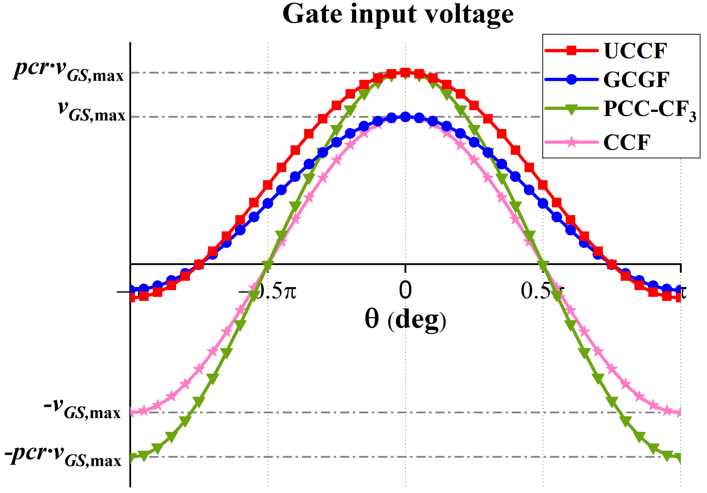
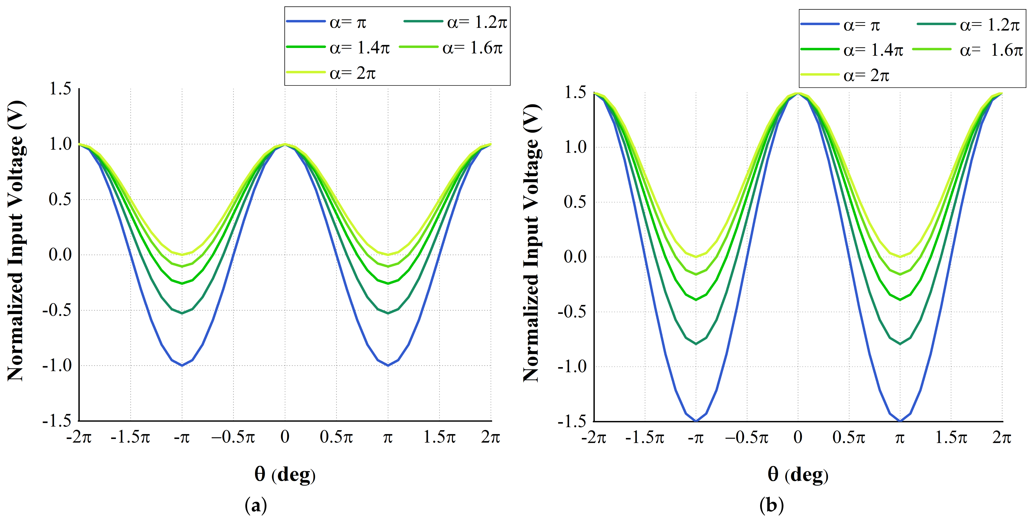
2.1. Gate Input Voltage Waveform of Proposed UCCF Mode

A transistor is a voltage-controlled current source, and a change in the gate input voltage waveform can lead to a change in the drain current waveform. Therefore, it is necessary to analyze the gate input voltage waveform first. The gate input voltage waveform of the UCCF mode ( v G S , U F ) in one signal period is shown in Figure 2 and can be represented as
v G S , U F = V G S 0 + V G S 1 × p c r × cos θ cos α 2 1 cos α 2
where V G S 0 is the gate threshold voltage, V G S 1 is the gate input voltage fundamental component, p c r refers to the peak-clipped ratio, θ denotes the angular phase of the cosine wave, and α denotes the drain current conduction angle. We rearranged the terms and normalized the gate input voltage using V G S 1 . The normalized gate input voltage v G S , n o r m could then be expressed as
v G S , n o r m = v G S , U F V G S 0 V G S 1 = p c r × cos θ cos α 2 1 cos α 2
where
p c r = v G S , U F V G S 0 v G S , m a x V G S 0
and v G S , m a x is the input voltage amplitude that just reaches the saturation point. Figure 2 depicts states of the gate input voltage waveform for various modes. As shown in Figure 2, the gate input voltage of the continuous class F (CCF) mode is an ideal cosine wave where α equals π and p c r equals 1. The GCCF mode achieves the finite third-harmonic load impedance by expanding α , and in this mode, p c r is equal to 1. The PCC-CF 3 mode achieves the finite third-harmonic load impedance by inputting an overdriven gate voltage, and in this mode, α is equal to π . To leverage the advantages of both modes, the UCCF mode combines p c r and α to reshape the drain current waveform. The GCCF and PCC-CF 3 modes are special cases of the UCCF mode.
Figure 3a,b illustrate the variationin v G S , n o r m with p c r and α . When p c r is the same, the peak-to-peak amplitude of v G S , n o r m decreases with an increase in α . When α stays the same, the peak-to-peak amplitude of v G S , n o r m increases with an increase in p c r . This indicates that both p c r and α affect the input power, as an increase in α decreases this parameter and an increase in p c r increases it. These opposing trends lead to the different effects of p c r and α on the PA’s performance.

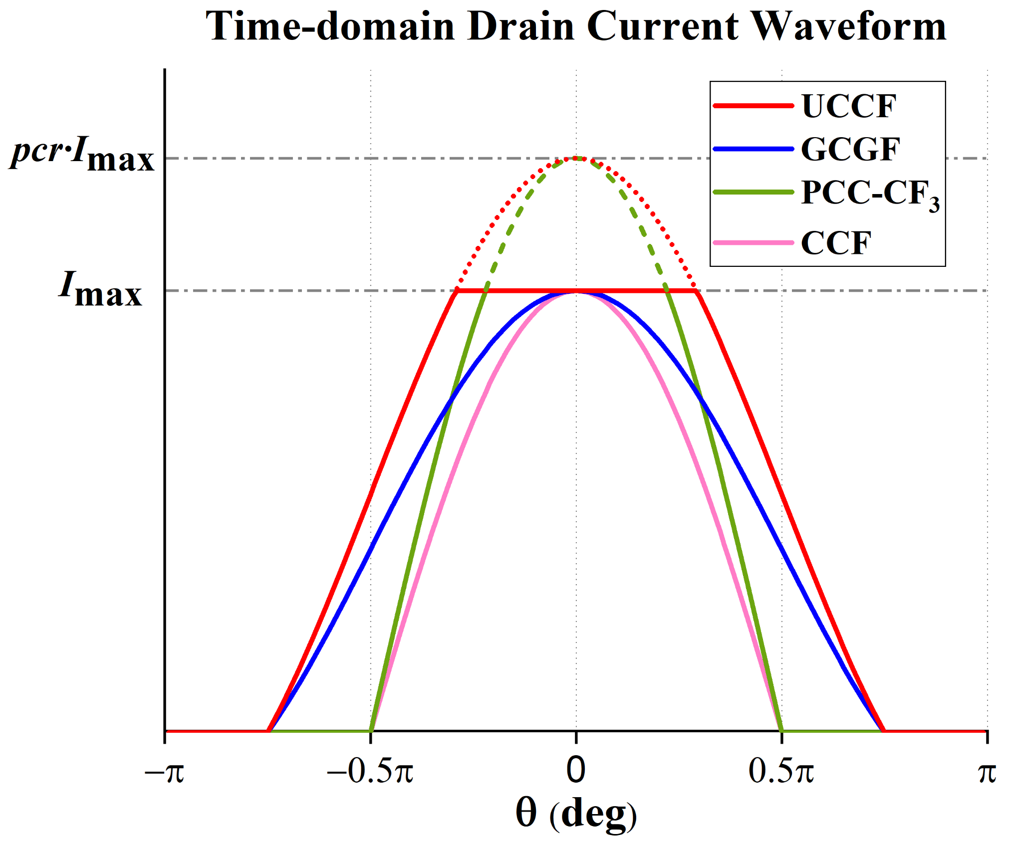
2.2. Drain Current Waveform of the Proposed UCCF Mode

The drain current waveform of the proposed UCCF mode ( i d , U F ) in one signal period (Figure 4) can be expressed as
i d , U F = I max × p c r × cos θ cos α 2 1 cos α 2 , α 2 < θ < β 2 I max , β 2 < θ < β 2 I max × p c r × cos θ cos α 2 1 cos α 2 , β 2 < θ < α 2 0 , π < θ < α 2 , α 2 < θ < π
where
β 2 = arccos 1 cos ( α 2 ) + p c r × cos α 2 p c r
and I max is the maximum drain current amplitude, and β is the angle at which the current waveform reaches I max . Figure 4 depicts the drain current waveform state for various modes. When p c r ranges from 1 to 2 and α ranges from π to 2 π in (4), the GCCF mode is present, and the drain current waveform is peak−clipped with a drain current conduction angle α of greater than π . When p c r equals 1 and α ranges from π to 2 π in (4), the GCCF mode is present, and the drain current waveform forms a half-sinusoidal wave with α greater than π . When p c r ranges from 1 to 2 and α equals π in (4), the PCC-CF 3 mode is present, and the drain current waveform exhibits a peak-clipped drain current waveform. When p c r equals 1 and α equals π in (4), the continuous class F mode is present, and the drain current waveform is an ideal half-sinusoidal wave.
The Fourier-series expansion of i d , U F [11] can be calculated as functions of p c r and α by (6)–(8),
i d , U F = I d c + n = 1 I n · cos n θ
where
I d c = 1 2 π · I max · 0 2 π i d , U F · cos n θ d θ , ( n = 0 )
I n = 1 π · I max · 0 2 π i d , U F · cos n θ d θ , ( n = 1 , 2 , 3 )
I d c = csc 2 α 4 β + β 1 + p c r α · p c r cos α 2 2 p c r · sin β 2 + 2 p c r · sin α 2 4 π I 1 = 8 sin β 2 p c r · csc 2 α 4 β α 4 cos α 2 sin β 2 + sin β + sin α 4 π I 2 = 3 sin β + p c r · csc 2 α 4 · sin 2 β α 4 3 sin β 2 + 2 · sin β + α 2 + sin β 2 + α 3 π I 3 = p c r · csc 2 α 4 3 1 + cos β sin β + 4 cos α 2 sin 3 β 2 + 8 sin 3 β 2 + p c r · csc 2 α 4 sin α 12 π
Through (9), the DC ( I d c ), fundamental ( I 1 ), second-harmonic ( I 2 ), and third-harmonic ( I 3 ) components can be computed. Figure 5 illustrates the I d c , I 1 , I 2 , and I 3 trends in the UCCF mode with p c r and α . The origin of the coordinates represents the continuous class F mode ( α = π and p c r = 1 ). The horizontal axis represents the GCCF mode with α values varying from π to 2 π ( p c r = 1 ). The vertical axis represents the PCC-CF 3 mode with p c r values varying from 1 to 2 ( α = π ). The color depth in the graph represents the magnitude of the current component. As shown in Figure 5a, I d c increases with increases in p c r and α . Figure 5b shows that when p c r is held constant, I 1 initially increases and then decreases with an increase in α . Figure 5c shows that I 2 decreases with increases in p c r and α . Figure 5d shows that when p c r is held constant, I 3 initially decreases and then increases with an increase in α . The blue area in the upper left corner of Figure 5d shows that I 3 has reached its minimum area. The minimum value of I 3 in the UCCF mode is −0.179, and this occurs when p c r is equal to 2 and α is equal to 1.184 π . In this region, I 3 is smaller than the horizontal and vertical axes, which indicates that the UCCF mode achieves a smaller I 3 compared to the GCCF and PCC-CF 3 modes.

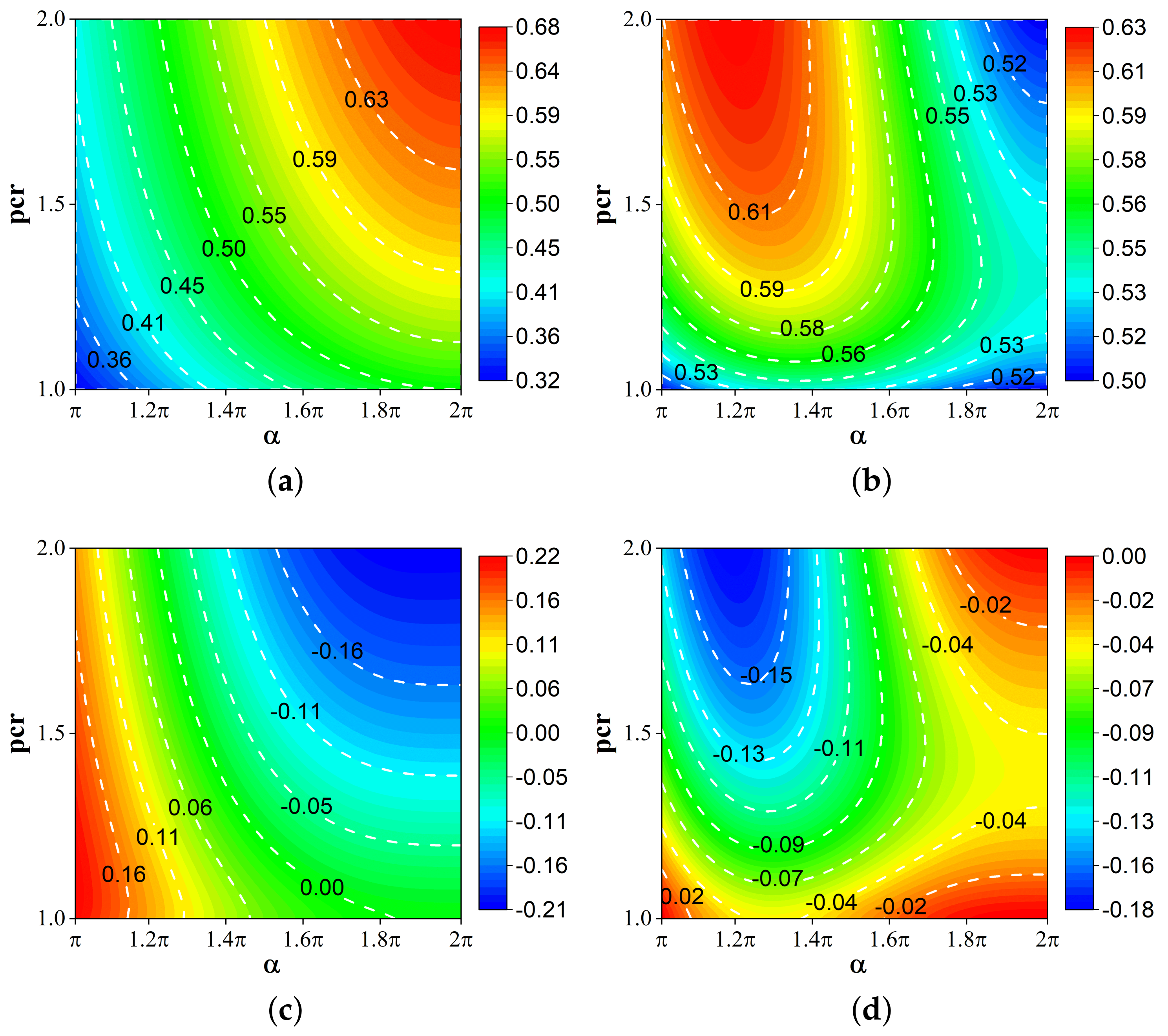
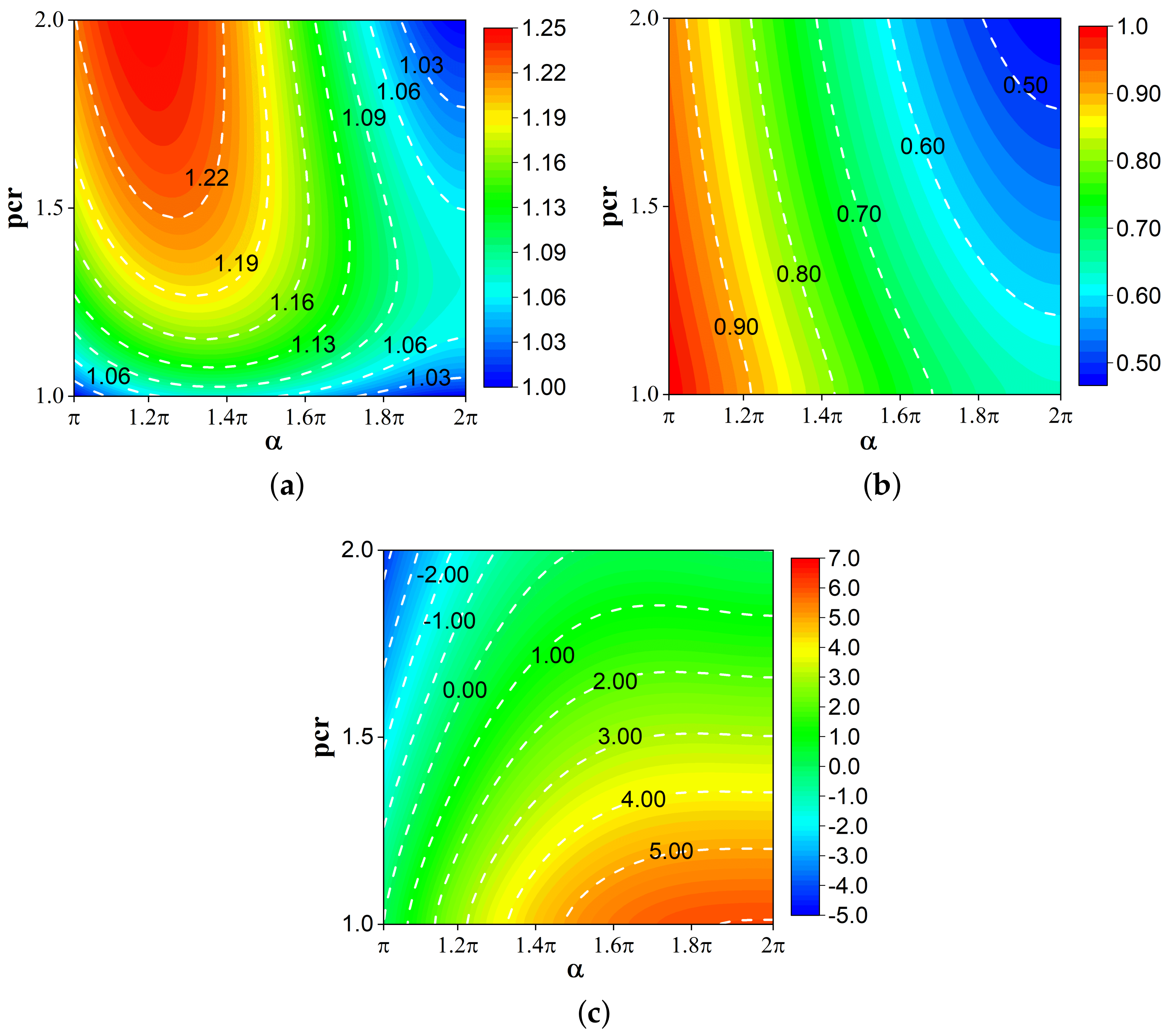
2.3. Load Impedance Design Space of the Proposed UCCF Mode

The drain voltage in the UCCF mode v d [32] is the same as that in the continuous class F mode and can be calculated using
v d = V k + ( V d d V k ) 1 2 3 cos θ 2 1 + 1 3 cos θ × 1 + γ sin θ , 1 < γ < 1
where V d d represents the drain bias voltage, V k represents the knee voltage of the transistor, and γ is the correction factor. The load impedance design space can be obtained as follows:
Z f 0 = 1 3 I 1 · R o p t + j γ 2 · I 1 · R o p t Z 2 f 0 = j 7 · γ 12 3 · I 2 · R o p t Z 3 f 0 = 1 6 3 I 3 · R o p t
where
R o p t = 2 V d d V k I max
R o p t is the optimal fundamental load impedance, and Z f 0 , Z 2 f 0 , and Z 3 f 0 are the fundamental, second-, and third-harmonic load impedances of the UCCF mode, respectively.
Equation (11) implies that the broader range of I 3 leads to a broader design space for the third-harmonic load impedance. The range of I 3 is 0 to −0.047 in the GCCF mode, 0 to −0.137 in the PCC-CF 3 mode, and 0 to −0.179 in the UCCF mode. The UCCF mode can produce smaller I 3 values, indicating that compared to the other two modes, it offers a broader third-harmonic load impedance design space.
As shown in Figure 6, the real part of the fundamental impedance Z f 0 varies with p c r and α , and the imaginary part varies with γ . The Z f 0 and Z 3 f 0 of the GCCF mode are highlighted in blue, whereas the expanded Z f 0 and Z 3 f 0 relative to the GCCF mode in the PCC-CF 3 mode are marked in green. Additionally, the expanded Z f 0 and Z 3 f 0 relative to the PCC-CF 3 mode in the UCCF mode are denoted in red. The real part of the second harmonic load impedance is zero, and the imaginary part varies with p c r , α , and γ . The Z 2 f 0 of the UCCF mode remains consistent with the GCCF mode, while the Z 2 f 0 of the GCCF mode is highlighted in blue. This shows that the UCCF mode expands not only the finite third-harmonic load impedance design space but also the fundamental and second harmonic load impedance design space.

2.4. Performance of Proposed UCCF Mode

The output power P o u t [29] and drain efficiency D E can be calculated from the drain current and voltage equations, which are functions of p c r and α . They can be expressed as
P o u t = 1 2 I 1 2 · Z f 0
D E = P o u t P D C
The trend of P o u t / P 0 and D E / D E 0 with p c r and α can be visualized in Figure 7a,b. P 0 and D E 0 represent the output power and efficiency of the continuous class F mode, respectively. In Figure 7, the coordinate origin represents the continuous class F mode, the horizontal axis represents the GCCF mode, and the vertical axis represents the PCC-CF 3 mode. At the coordinate origin, P o u t / P 0 and D E / D E 0 equal 1, as expected. It can be seen from Figure 7a that P o u t / P 0 is greater than 1, and increasing p c r and α can effectively enhance the output power. The range of P o u t / P 0 is 1 to 1.07 for the GCCF mode, 1 to 1.218 for the PCC-CF 3 mode, and 1 to 1.25 for the UCCF mode. This shows that compared with the GCCF and PCC-CF modes, the UCCF mode has a greater ability to improve the output power. In Figure 7b, it is obvious that increasing p c r and α leads to a decrease in the efficiency, and this trend becomes more pronounced as α increases. The D E / D E 0 drops from 1 to 63% in the GCCF mode and from 1 to 92.6% in the PCC-CF 3 mode.
The amplitude-to-amplitude modulation (AM/AM) at saturation is used as the evaluation criterion for linearity. AM / AM U represents the AM/AM of the UCCF mode, and AM / AM F represents the AM/AM of the continuous class F mode. AM / AM U and AM / AM F [29] can be expressed as
AM / AM U = G U G S
AM / AM F = G F G S
G U = 10 log P o u t P i n
G F = 10 log P 0 P i n
where G S is the small signal gain, G U is the power gain of the UCCF mode at saturation, and P i n is the input power.
AM / AM U AM / AM F = 20 log 10 2 I 1 1 cos α 2 p c r
Figure 7c shows the trend of AM / AM U AM / AM F with different p c r and α values. At the coordinate origin, AM / AM U AM / AM F equals 0, as expected. When AM / AM U AM / AM F is greater than 0, the linearity is better than that of the continuous class F PA. When AM / AM U AM / AM F is less than 0, the linearity is worse than that of the continuous class F PA. The range of AM / AM U AM / AM F is 1 to 6 in the GCCF mode and 1 to −4.3 in the PCC-CF 3 mode. As shown in Figure 7c, as α increases, AM / AM U AM / AM F increases, but as p c r increases, AM / AM U AM / AM F decreases. Therefore, the AM/AM distortion caused by an increase in p c r can be offset by selecting the appropriate α .

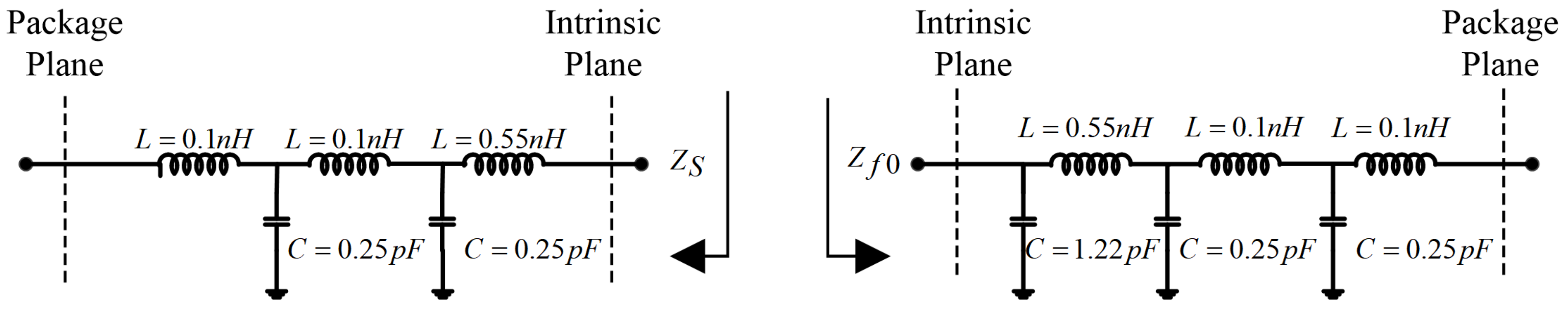
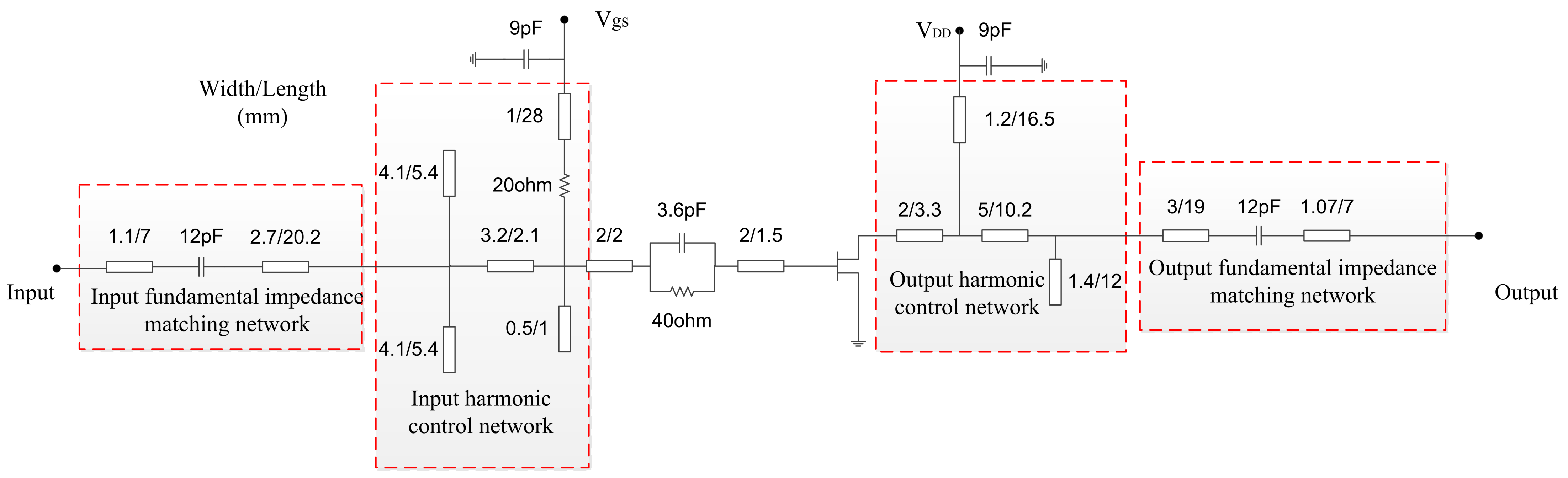
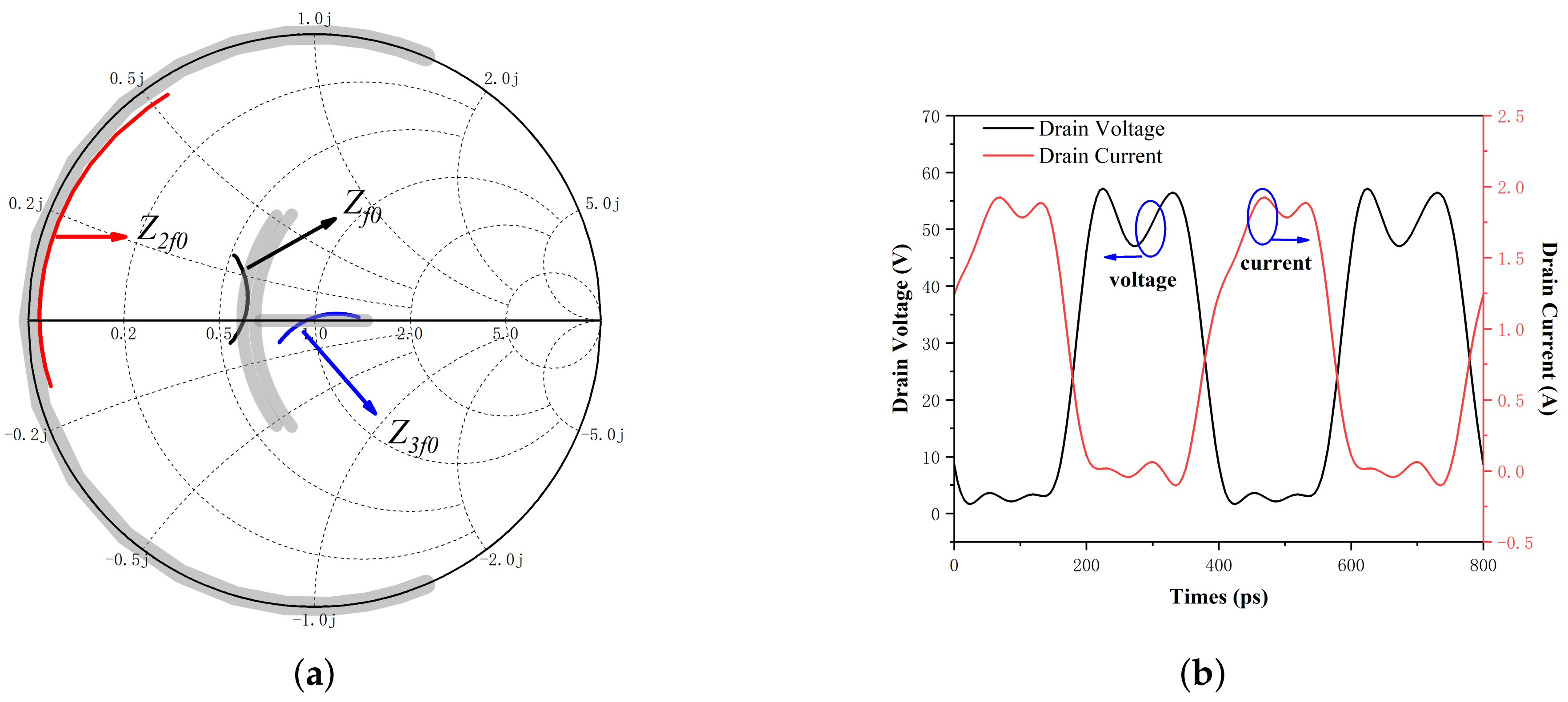
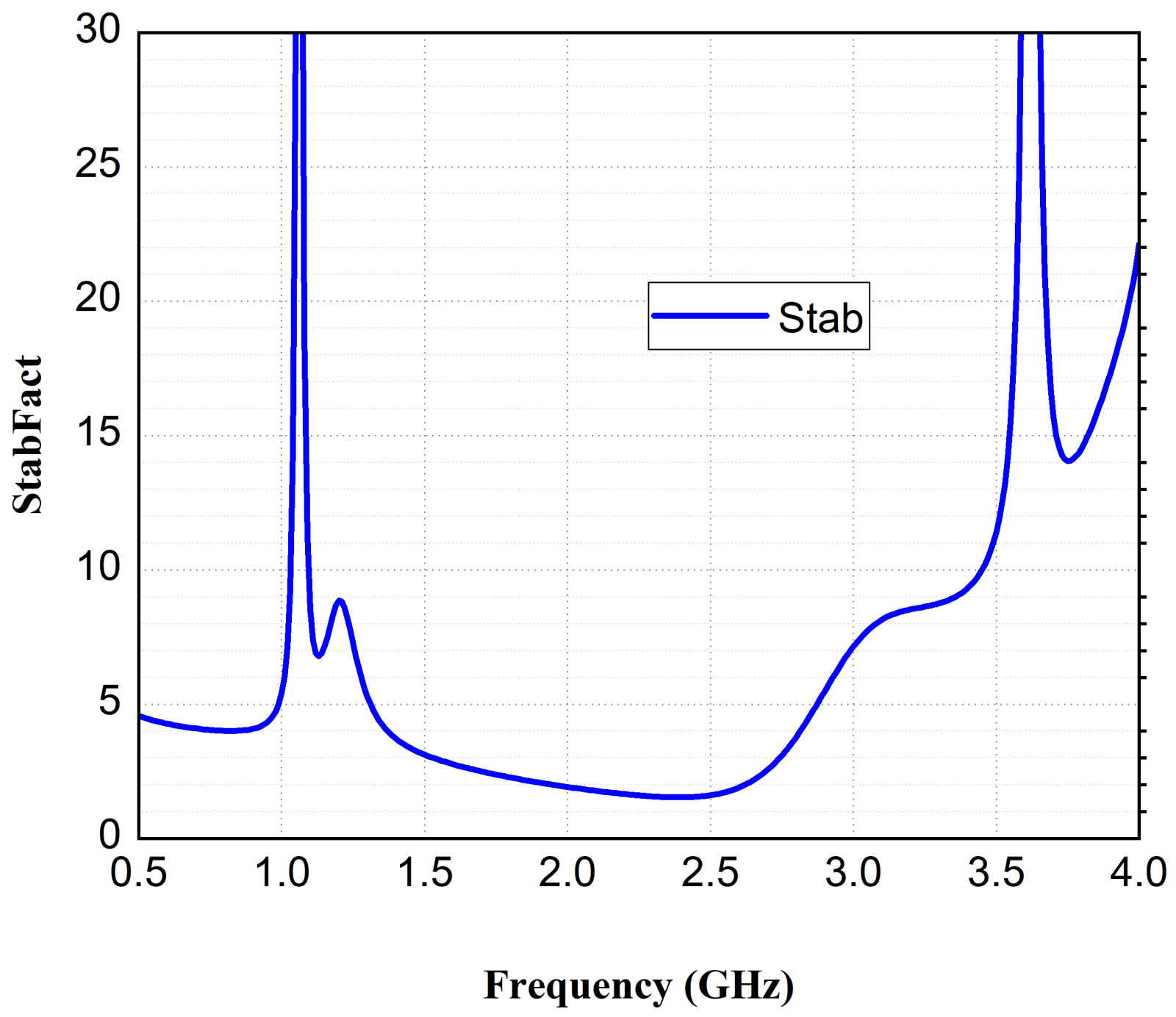
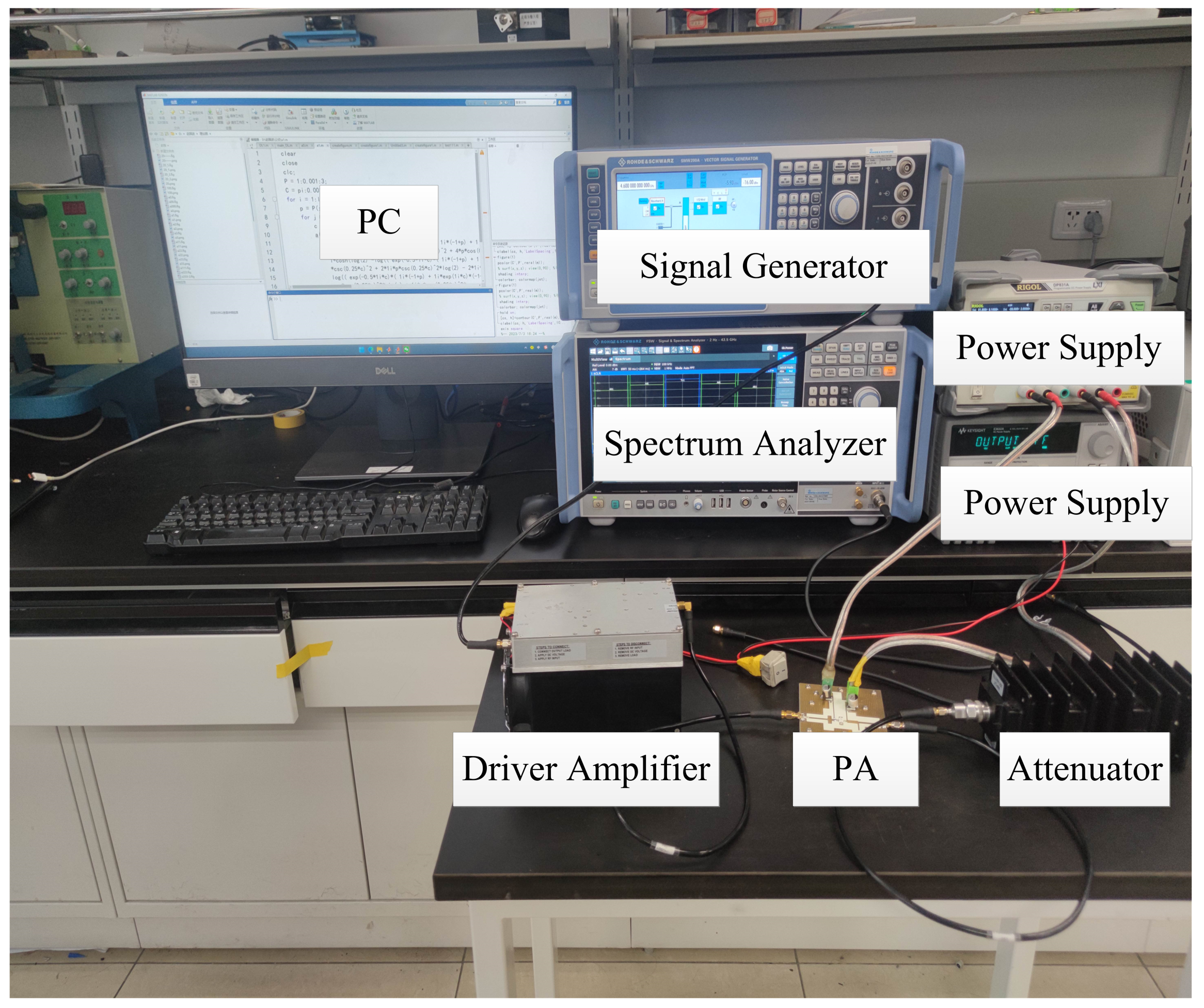
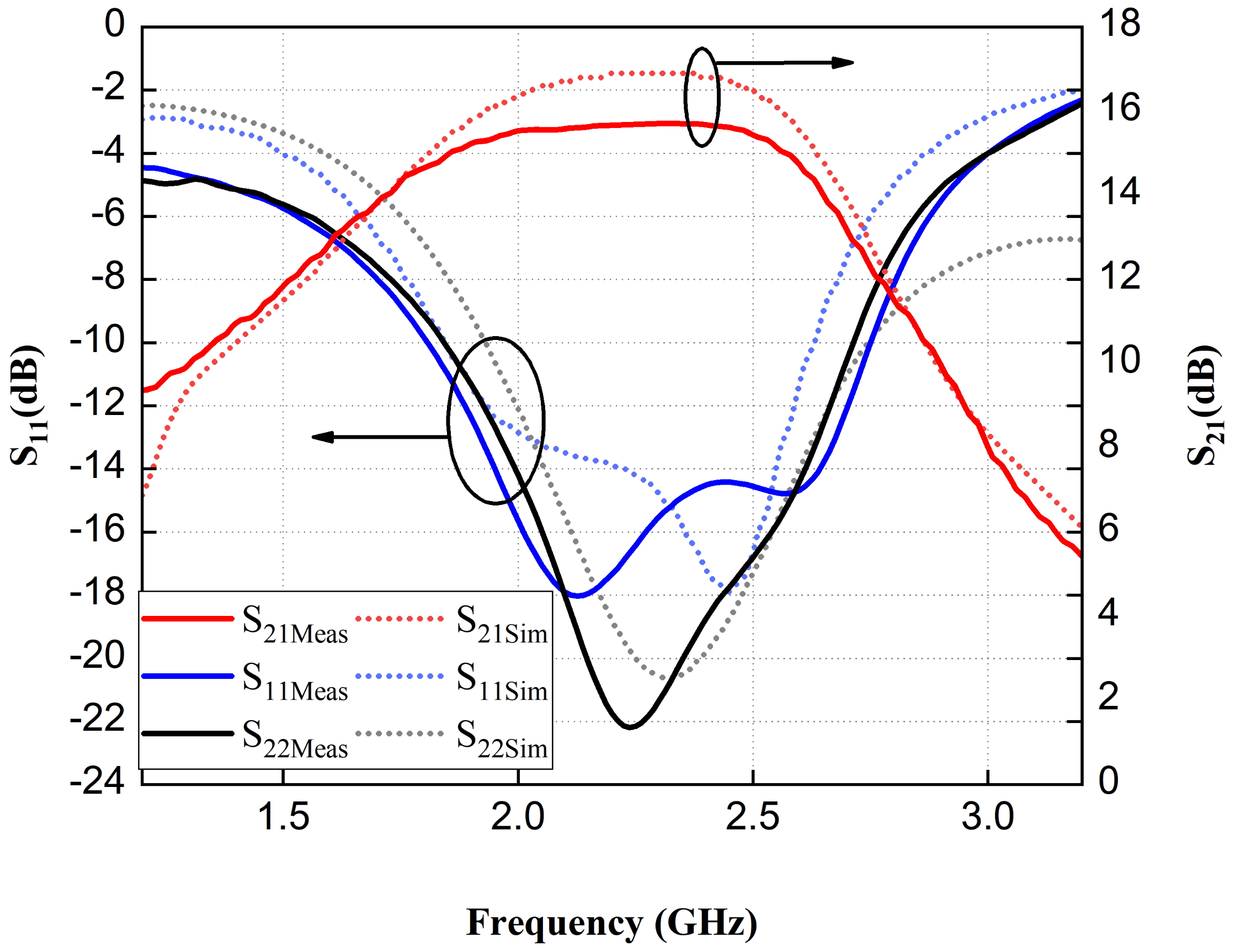
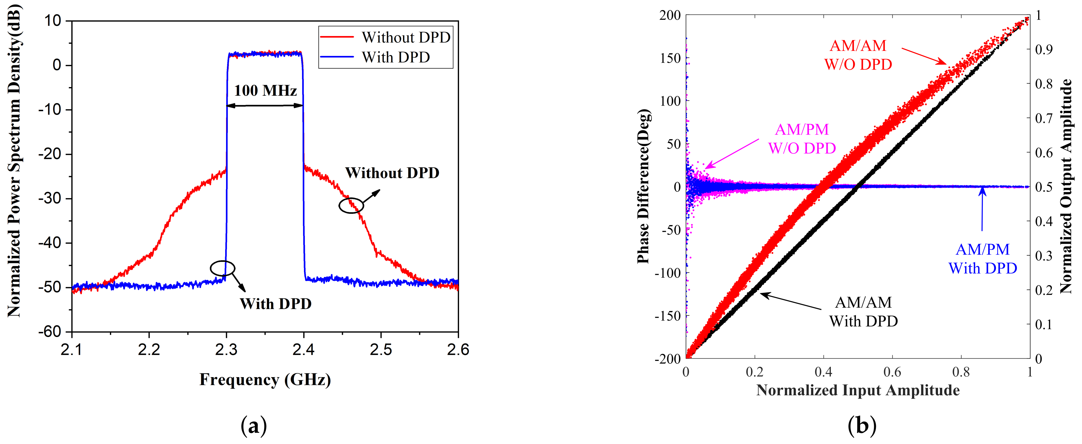
3. Fabrication and Measurement Result of the Proposed UCCF Mode PA

The UCCF mode enables a broader finite third-harmonic load impedance space and a better balance between efficiency and linearity. To verify this theory, the PA was designed based on CREE’s CGH40010F GaN HEMT with an output power of 10 W and an optimal impedance of 30 Ω .
The key issue when implementing the UCCF mode is the correct selection of p c r and α . When choosing p c r and α , it is necessary to comprehensively consider the efficiency and linearity. In this design, p c r and α were selected according to the conditions listed in (19),
AM / AM U AM / AM F 0 D E / D E 0 0.9 P o u t / P 0 1
In Figure 8, the blue region indicates AM / AM U AM / AM F 0 , while the green region indicates D E / D E 0 0.9 . The gray line in Figure 8 represents the contour line of I 3 . From Figure 7a, it can be observed that P o u t / P 0 is greater than 1 throughout the entire plot. When choosing p c r and α , it is necessary to ensure that they fall in the overlapping area, called the operating space in Figure 8, to achieve a balance between efficiency and linearity.
A schematic of the PA with the drain bias voltage set to V D D = 28 V and the quiescent drain current set to 265 mA is shown in Figure 9. Since the theoretical analysis is conducted in the current source plane, parasitic parameter models [33] are required to transform the packaging plane into the current source plane. In this design, α equals 1.17 π and p c r ranges from 1 to 1.2. The corresponding impedance space is shown in Figure 10. The working state used in this design has enhanced linearity and acceptable efficiency. The impedance trajectory of this design, shown in Figure 10a, aligns with the impedance space. In Figure 10b, the simulated voltage and current waveforms of the current source plane are depicted and are consistent with the theoretical design. As shown in Figure 11, the stability factor is close to 1 and greater than 1 in 2–2.6 GHz, and the stability factor is greater than 1 in the whole frequency band, which proves that the designed PA has good stability.
As shown in Figure 12, the measurement setup includes a signal generator (SMW200A), a spectrum analyzer (FSW-43), two power supplies (E3632A, DP832A), a driver amplifier (ZHL-16W-43-S+PA), a DUT, an attenuator, and a PC. The layout design of the PA is shown in Figure 13, and the circuit size is 8.8 cm × 8.6 cm. A Rogers 4350B with a thickness of 20 mils and a dielectric constant of 3.66 was used as the substrate. As shown in Figure 14, S-parameters were measured at 2.05–2.65 GHz using an Agilent N5230C vector network analyzer.
The test results indicate that S 21 is greater than 14 dB, S 11 is less than −14 dB and S 22 is less than −12 dB. Figure 15a depicts the variations in the drain efficiency and gain with theoutput power, and Figure 15b depicts the variations in the drain output power, efficiency, and gain with the frequency. The results show that the drain efficiency was 67.0–73.2%, the output power was 40.1–41.0 dBm, and the gain was 9–10.8 dB. The DPD test platform is shown in Figure 12, which includes te signal generator, spectrum analyzer, power supplies, driver amplifier, PA, attenuator, and PC. A 5G NR (New Radio) signal with a 100 MHz bandwidth (the peak average power ratio was 8 dB) was used to test the PA’s output spectrum at 2.35 GHz. The DPD in this paper adopts the GMP model and utilizes the indirect structure. K a = 5 and L a = 6 are the index arrays for the aligned signal and envelope; K b = 5 , L b = 6 and M b = 2 are the index arrays for the signal and lagging envelope; and, K c = 5 , L c = 6 and M c = 2 are index arrays for the signal and leading envelope. The algorithm part is processed in MATLAB, 10,000 samples are used for fitting, and another 10,000 samples are used for verification. As shown in Figure 16a, the worst ACPR was −34.8 dBc without digital predistortion (DPD) and −57.8 dBc with DPD. There was an average output power ( P a v e ) of around 32.4 dB and an average DE ( D E a v e ) of 34.39%. This shows that the UCCF mode performs well in terms of the adjacent channel interference. Figure 16b shows the PA’s amplitude-to-amplitude modulation (AM/AM) and amplitude-to-phase modulation (AM/PM) characteristics with and without DPD. Through testing, it can be seen that the designed PA has good linearity.
Table 1 presents the performance comparison with other PAs. All comparison designs are based on 10 W PA tubes. In both [34] and this work, a 100 MHz bandwidth signal was employed for spectrum testing. The ACPR presented in [34] is 11.81 dB worse than that shown in this work without DPD The P ave and DE ave of [34] are lower than that those in the UCCF mode. Although the ACPR values presented in [26,30,35,36] are comparable with those shown for the UCCF mode, the signal bandwidth was found to be relatively narrow when testing the spectrum. Moreover, in [23,37,38], the ACPR tested with a narrow bandwidth signal was worse than that measured in the UCCF mode. This shows that the proposed UCCF mode stands out due to its superior linearity. The efficiency of the UCCF mode is comparable with that shown in other works. This design effectively strikes a better balance between efficiency and linearity compared to other PAs.

4. Conclusions

In this paper, the UCCF mode, which extends the flexibility of the PA working state by considering the influence of conduction angle and overdriven transistor on the current waveform, was proposed. Following rigorous theoretical derivations, the load impedance design space tailored to the UCCF mode was deduced. Subsequently, the efficiency and linearity characteristics of this mode were comprehensively analyzed, and a balanced PA performance was achieved. The empirical test results strongly support the effectiveness of this new mode, closely aligning with our anticipated outcomes. This positions the UCCF mode as an excellent performance choice with the potential for widespread applications.

Author Contributions

Conceptualization, F.L.; methodology, F.L.; software, F.L.; validation, F.L.; formal analysis, F.L.; investigation, F.L.; resources, F.L.; data curation, F.L.; writing—original draft preparation, F.L.; writing—review and editing, C.Y.; visualization, C.Y.; supervision, C.Y.; project administration, C.Y.; funding acquisition, C.Y. All authors have read and agreed to the published version of the manuscript.

Funding

This research was funded by the National Natural Science Foundation of China under Grant 62090015 and Grant 61821001 and by the Shenzhen Science and Technology Program CJGJZD20210408092001003.

Institutional Review Board Statement

Not applicable.

Informed Consent Statement

Not applicable.

Data Availability Statement

The original contributions presented in the study are included in the article, further inquiries can be directed to the corresponding author.

Conflicts of Interest

The authors declare no conflicts of interest.

References

  1. Li, X.; Helaoui, M.; Ghannouchi, F.M.; Zhao, Y.; Liu, C.; Chen, W.; Sharawi, M.S. A class-X power amplifier with finite number of harmonics. IEEE Trans. Microw. Theory Tech. 2022, 70, 3897–3909. [Google Scholar] [CrossRef]
  2. Poluri, N.; Souza, M.M.D. High-efficiency modes contiguous with class B/J and continuous class F−1 amplifiers. IEEE Microw. Wireless Compon. Lett. 2019, 29, 137–139. [Google Scholar] [CrossRef]
  3. Wright, P.; Lees, J.; Benedikt, J.; Tasker, P.J.; Cripps, S.C. A methodology for realizing high efficiency class-J in a linear and broadband PA. IEEE Trans. Microw. Theory Tech. 2009, 57, 3196–3204. [Google Scholar] [CrossRef]
  4. Rezaei, S.; Belostotski, L.; Helaoui, M.; Ghannouchi, F.M. Harmonically tuned continuous class-C operation mode for power amplifier applications. IEEE Trans. Microw. Theory Tech. 2014, 62, 3017–3027. [Google Scholar] [CrossRef]
  5. Carrubba, V.; Clarke, A.L.; Akmal, M.; Yusoff, Z.; Lees, J.; Benedikt, J.; Cripps, S.C.; Tasker, P.J. Exploring the design space for broadband PAs using the novel continuous inverse class-F mode. In Proceedings of the 2011 41st European Microwave Conference, Manchester, UK, 10–13 October 2011; pp. 10–13. [Google Scholar]
  6. Alizadeh, A.; Medi, A. Investigation of a class-J mode power amplifier in presence of a second-harmonic voltage at the gate node of the transistor. IEEE Trans. Microw. Theory Tech. 2017, 65, 3024–3033. [Google Scholar] [CrossRef]
  7. Huang, C.; He, S.; Shi, W.; Song, B. Design of broadband high efficiency power amplifiers based on the hybrid continuous modes with phase shift parameter. IEEE Microw. Wireless Compon. Lett. 2018, 28, 159–161. [Google Scholar] [CrossRef]
  8. Abbasian, S.; Johnson, T. Power-Efficiency characteristics of class-F and inverse class-F synchronous rectifiers. IEEE Trans. Microw. Theory Tech. 2016, 64, 4740–4751. [Google Scholar] [CrossRef]
  9. Kim, J.H.; Lee, S.J.; Park, B.H.; Jang, S.H.; Jung, J.H.; Park, C.S. Analysis of high-efficiency power amplifier using second harmonic manipulation: Inverse class-F/J amplifiers. IEEE Trans. Microw. Theory Tech. 2011, 59, 2024–2036. [Google Scholar] [CrossRef]
  10. Krauss, H.L.; Bostain, C.W.; Raab, F.H. Solid State Radio Engineering; Wiley: New York, NY, USA, 1980. [Google Scholar]
  11. Cripps, S.C. RF Power Amplifier for Wireless Communication, 2nd ed.; Artech House: Norwood, MA, USA, 2006. [Google Scholar]
  12. Carrubba, V.; Clarke, A.L.; Akmal, M.; Lees, J.; Benedikt, J.; Tasker, P.J.; Cripps, S.C. The continuous class-F mode power amplifier. In Proceedings of the 5th European Microwave Integrated Circuits Conference, Paris, France, 27–28 September 2010; pp. 432–435. [Google Scholar]
  13. Gao, S. High efficiency class-F RF/microwave power amplifiers. IEEE Microw. Mag. 2006, 7, 40–48. [Google Scholar] [CrossRef]
  14. Chen, K.; Peroulis, D. A 3.1-GHz class-F power amplifier with 82% power-added-efficiency. IEEE Microw. Wireless Compon. Lett. 2013, 23, 436–438. [Google Scholar] [CrossRef]
  15. Raab, F.H. Maximum efficiency and output of class-F power amplifiers. IEEE Trans. Microw. Theory Tech. 2001, 49, 1162–1166. [Google Scholar] [CrossRef]
  16. Grebennikov, A.; Raab, F.H. History of Class-F and inverse Class-F techniques: Developments in high–efficiency power amplification from the 1910s to the 1980s. IEEE Microw. Mag. 2018, 19, 99–115. [Google Scholar] [CrossRef]
  17. Woo, Y.Y.; Yang, Y.; Kim, B. Analysis and experiments for high-efficiency class-F and inverse class-F power amplifiers. IEEE Trans. Microwave Theory Tech. 2006, 54, 1969–1974. [Google Scholar]
  18. Raab, F.H. Class-E, class-C, and class-F power amplifiers based upon a finite number of harmonics. IEEE Trans. Microw. Theory Tech. 2001, 49, 1462–1468. [Google Scholar] [CrossRef]
  19. Dhar, S.K.; Sharma, T.; Zhu, N.; Darraji, R.; Mclaren, R.; Holmes, D.G.; Mallette, V.; Ghannouchi, F.M. Input-Harmonic-Controlled broadband continuous class-F power amplifiers for sub-6-GHz 5G applications. IEEE Trans. Microw. Theory Tech. 2020, 68, 3120–3133. [Google Scholar] [CrossRef]
  20. Zheng, S.; Liu, Z.; Zhang, X.; Zhou, X.; Chan, W. Design of ultra- wideband high-efficiency extended continuous class-F power amplifier. IEEE Trans. Ind. Electron. 2018, 65, 4661–4669. [Google Scholar] [CrossRef]
  21. Chen, K.; Peroulis, D. Design of broadband highly efficient harmonic-tuned power amplifier using in-band continuous class-F−1/F mode transferring. IEEE Trans. Microw. Theory Tech. 2012, 60, 4107–4116. [Google Scholar] [CrossRef]
  22. Chen, J.; He, S.; You, F.; Tong, R.; Peng, R. Design of broadband high efficiency power amplifiers based on a series of continuous modes. IEEE Microw. Compon. Lett. 2014, 24, 631–633. [Google Scholar] [CrossRef]
  23. Tuffy, N.; Guan, L.; Zhu, A.; Brazil, T.J. A simplified broadband design methodology for linearized high-efficiency continuous class–F power amplifiers. IEEE Trans. Microw. Theory Tech. 2012, 60, 1952–1963. [Google Scholar] [CrossRef]
  24. Miura, O.; Ishikawa, R.; Honjo, K. Parasitic-element compensation based on factorization method for microwave inverse class-F/class-F amplifiers. IEEE Microw. Wireless Compon. Lett. 2012, 22, 521–523. [Google Scholar] [CrossRef]
  25. Kuroda, K.; Ishikawa, R.; Honjo, K. Parasitic compensation design technique for a C-band GaN HEMT class-F amplifier. IEEE Trans. Microw. Theory Tech. 2010, 58, 2741–2750. [Google Scholar] [CrossRef]
  26. Dong, Y.; Mao, L.; Xie, S. Extended continuous inverse class-F power amplifiers with class-AB bias conditions. IEEE Microw. Wireless Compon. Lett. 2017, 27, 368–370. [Google Scholar] [CrossRef]
  27. Moon, J.; Jee, S.; Kim, J.; Kim, J.; Kim, B. Behaviors of Class-F and Class-F−1 Amplifiers. IEEE Trans. Microw. Theory Tech. 2012, 60, 1937–1951. [Google Scholar] [CrossRef]
  28. Sharma, T.; Darraji, R.; Ghannouchi, F.; Dawar, N. Generalized continuous class-F harmonic tuned power amplifiers. IEEE Microw. Wireless Compon. Lett. 2016, 26, 213–215. [Google Scholar] [CrossRef]
  29. Kim, J.H.; Jo, G.D.; Oh, J.H.; Kim, Y.H.; Lee, K.C.; Jung, J.H. Modeling and design methodology of high-efficiency class-F and class-F−1 power amplifiers. IEEE Trans. Microw. Theory Tech. 2011, 59, 153–165. [Google Scholar] [CrossRef]
  30. Han, K.; Geng, L. Enhancing efficiency and linearity of continuous class-F3 power amplifier with peak-clipped current waveform. IEEE Trans. Microw. Theory Tech. 2022, 70, 1423–1431. [Google Scholar] [CrossRef]
  31. Tasker, P.; Benedikt, J. Waveform inspired models and the harmonic balance emulator. IEEE Microw. Mag. 2011, 12, 38–54. [Google Scholar] [CrossRef]
  32. Carrubba, V.; Lees, I.; Benedikt, J.; Tasker, P.J.; Cripps, S.C. A Novel Highly Efficient Broadband Continuous Class-F RFPADelivering 74% Average Efficiency for an Octave Bandwidth. In Proceedings of the 2011 IEEE MTT-S International Microwave Symposium, Baltimore, MD, USA, 5–10 June 2011. [Google Scholar]
  33. Li, X.; Helaoui, M.; Ghannouchi, F. Optimal fundamental load modulation for harmonically tuned switch mode power amplifier. In Proceedings of the 2016 IEEE MTT-S International Microwave Symposium (IMS), San Francisco, CA, USA, 22–27 May 2016; pp. 1–4. [Google Scholar]
  34. Chu, C.; Tamrakar, V.; Dhar, S.K.; Sharma, T.; Mukherjee, J.; Zhu, A. High-efficiency class-iF−1 power amplifier with enhanced linearity. IEEE Trans. Microw. Theory Tech. 2023, 71, 1977–1989. [Google Scholar] [CrossRef]
  35. Li, S.; Wu, Y.; Yang, Y.; Chen, X.; Wang, W.; Chen, Z. Bandpass filtering power amplifier with wide stopband and high out-of-band rejection. IEEE Trans. Circuits Syst. II Exp. Briefs 2023, 70, 969–973. [Google Scholar] [CrossRef]
  36. Haider, M.F.; You, F.; Qi, T.; Li, C.; Ahmad, S. Co-Design of second harmonic-tuned power amplifier and a parallel-coupled stub loaded resonator. IEEE Trans. Circuits Syst. II Exp. Briefs 2020, 67, 3013–3017. [Google Scholar] [CrossRef]
  37. Yang, M.; Xia, J.; Guo, Y.; Zhu, A. Highly efficient broadband continuous inverse class-F power amplifier design using modified elliptic low-pass filtering matching network. IEEE Trans. Microw. Theory Tech. 2016, 64, 1515–1525. [Google Scholar] [CrossRef]
  38. Eskandari, S.; Zhao, Y.; Helaoui, M.; Ghannouchi, F.M.; Kouki, A.B. Continuous-mode inverse class-GF power amplifier with second-harmonic impedance optimization at device input. IEEE Trans. Microw. Theory Tech. 2021, 69, 2506–2518. [Google Scholar] [CrossRef]
  39. Su, Z.; Yu, C.; Tang, B.; Liu, Y. Bandpass filtering power amplifier with extended band and high efficiency. IEEE Microw. Wireless Compon. Lett. 2020, 30, 181–184. [Google Scholar] [CrossRef]
  40. Guo, Q.-Y.; Zhang, X.Y.; Xu, J.-X.; Li, Y.C.; Xue, Q. Bandpass class-F power amplifier based on multifunction hybrid cavity–microstrip filter. IEEE Trans. Circuits Syst. II Exp. Briefs 2017, 64, 742–746. [Google Scholar] [CrossRef]
Figure 1. The parasitic parametric CGH40010F model [31].
Electronics 13 02284 g001
Figure 2. Gate input voltage waveforms with different modes.
Electronics 13 02284 g002
Figure 3. Gate input voltage of the UCCF mode ( v G S , n o r m ). (a) p c r equals 1, and α changes from π to 2 π . (b) p c r equals 1.5, and α changes from π to 2 π .
Electronics 13 02284 g003
Figure 4. Time domain drain current waveforms with different modes.
Electronics 13 02284 g004
Figure 5. Normalized drain current components, (a) I d c , (b) I 1 , (c) I 2 , and (d) I 3 .
Electronics 13 02284 g005
Figure 6. Load impedance design space with the UCCF mode.
Electronics 13 02284 g006
Figure 7. P o u t / P 0 , D E / D E 0 , and AM / AM U AM / AM F as functions of p c r and α . (a) P o u t / P 0 , (b) D E / D E 0 , (c) AM / AM U AM / AM F .
Electronics 13 02284 g007
Figure 8. Operating space in PA design.
Electronics 13 02284 g008
Figure 9. Complete schematic of the PA design.
Electronics 13 02284 g009
Figure 10. (a) Intrinsic load trajectories. (b) Simulated voltage and current waveforms on the PA’s current source plane.
Electronics 13 02284 g010
Figure 11. The stability curve of the proposed design.
Electronics 13 02284 g011
Figure 12. Measurement settings.
Electronics 13 02284 g012
Figure 13. Measurement. (a) Circuit layout with dimensions. (b) Layout of PA.
Electronics 13 02284 g013
Figure 14. Measured S-parameters.
Electronics 13 02284 g014
Figure 15. Large−signal measurement results from 2.05 to 2.65 GHz. (a) Efficiency and gain versus P o u t . (b) Efficiency, gain, and P o u t versus frequency.
Electronics 13 02284 g015
Figure 16. Linearity with and without DPD correction of the designed PA. (a) Measured PSD (power spectrum density). (b) Measured AM/AM and AM/PM.
Electronics 13 02284 g016
Table 1. Comparisons with previous works.
Refs.ModeFreq
(GHz)
Pout
(dBm)
DE
(%)
TransistorSubstrateSize
(cm × cm)
S11
(dB)
S22
(dB)
S21
(dB)
Pave
(dBm)
DEave
(%)
Signal BW
(MHz)
ACPR wo/w DPD (dBc)
(PAPR (dB))
[23]CCF1.45–2.4540.2–42.266–74.6CGH40010FTaconic RF35N/AN/AN/AN/A354640−24.9/−49.7 (N/A)
[26]GCCF0.5–0.9538–4073–79NXP AFT27S006NRogers 4003CN/AN/AN/AN/A3332–415−35/−43 (N/A)
[30] PCC-CF 3 1.6–1.841.6–4272–74CGH40010FRogers 4350B5.5 × 7N/AN/AN/A353420−34/−49 (6.5)
[39]Filtering2.0–2.439–40.469–78.2CG2H40010FRogers 4350B8 × 6−10N/A13.4–15.1N/AN/AN/AN/A
[35]Filtering1.85–2.138.6–3958.5–73CGH40010FRT/Duroid 5880N/A−10N/A13N/AN/A20−34.8/−57.8 (7)
[36]BJ1.6–2.84065–66CGH40010FRogers 4350B6.7 × 5.3N/AN/AN/A30.64N/A5−36.5/−55.8 (8.2)
[40]CF2.25–2.5140.851–67CGH40010FRogers 58808.1 × 2.9−10N/A17N/AN/AN/AN/A
[37] F 1 1.35–2.541.1–42.568–82CGH40010FTaconic RF35N/AN/AN/AN/A34.63720−26.4/−45.2 (7)
[38] CCGF 1 3.05–3.8539.9–41.470–78CG2H40010FDupont 9K7N/AN/AN/AN/A32N/A20−26/(N/A) (10.45)
[34] iF 1 2.0–2.640.1–40.871.2–77.3CG2H40010FTaconic TLY−5N/AN/AN/AN/A31.834.21100−22.99/−48.76 (8.5)
This workUCCF2.05–2.6540.1–4167.0–73.2CGH40010FRogers 4350B8.8 × 8.6−14−121432.434.39100−34.8/−57.8(8)
N/A: not available, iF 1 : a mode that utilizes input harmonics to enhance the linearity performance beyond that of the conventional Class-F 1 mode, CCGF 1 : continuous class GF 1 mode, CCF: continuous class F mode, CF: class F mode, Filtering: Filtering PA.
Disclaimer/Publisher’s Note: The statements, opinions and data contained in all publications are solely those of the individual author(s) and contributor(s) and not of MDPI and/or the editor(s). MDPI and/or the editor(s) disclaim responsibility for any injury to people or property resulting from any ideas, methods, instructions or products referred to in the content.

