
An Input-Series Output-Parallel DC–DC Converter Based on Fuzzy PID Three-Loop Control Strategy


Abstract
:1. Introduction
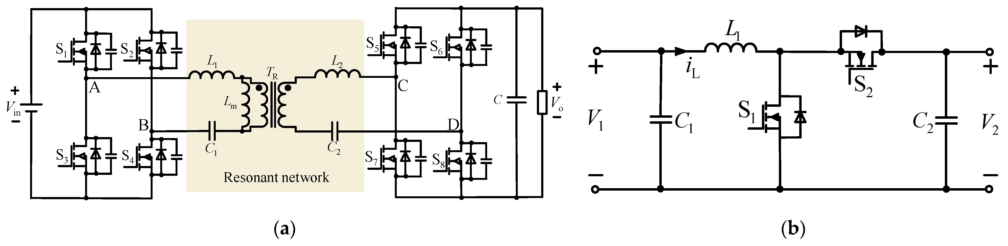
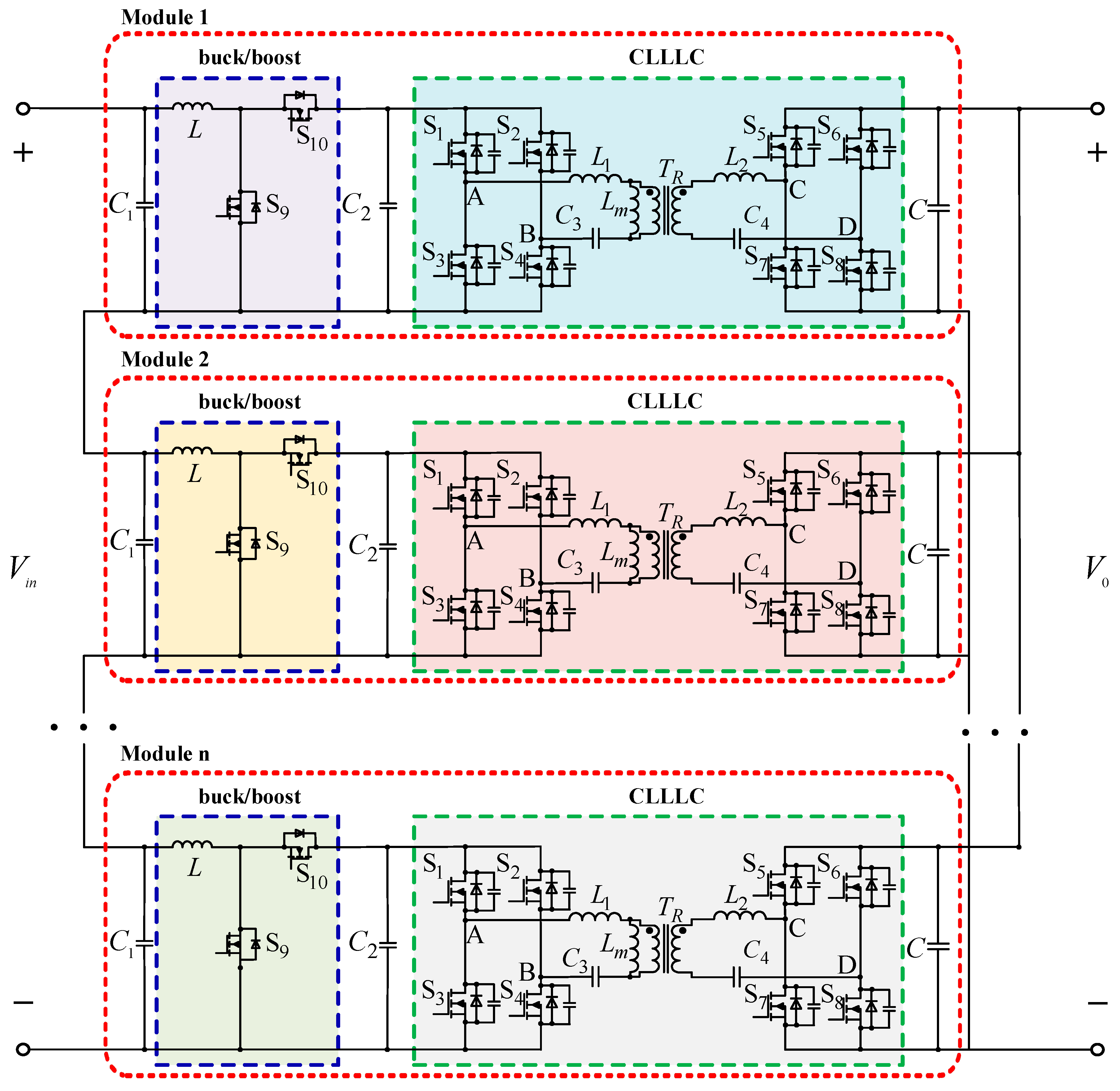
2. Converter Topology and System Structure
3. Cascade Converter Model, Characteristic Analysis, and Parameters Design
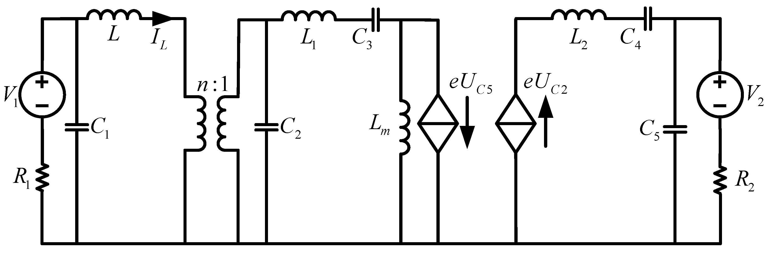
3.1. Establishment and Analysis of Mathematical Model for Cascade Converter
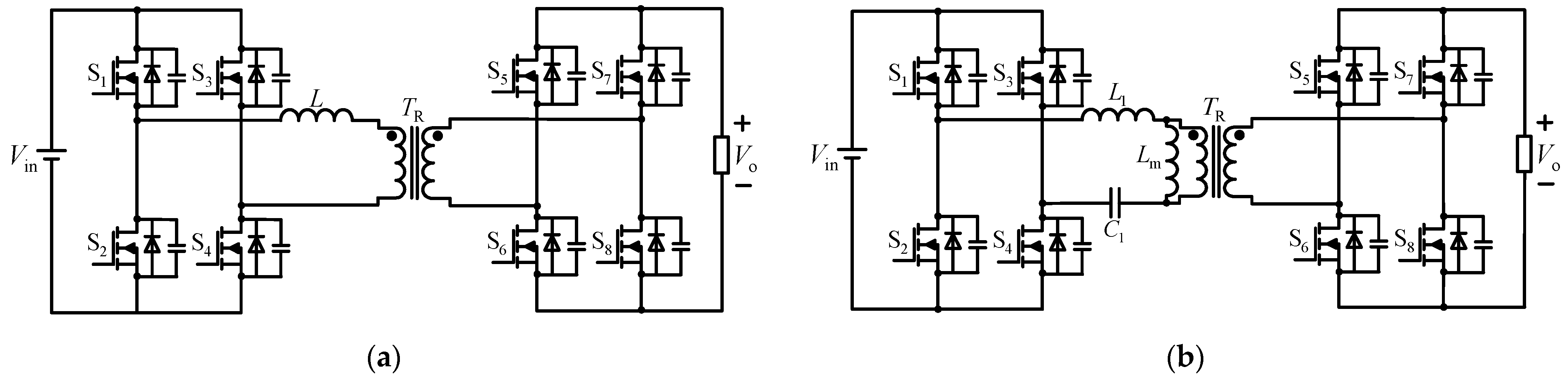
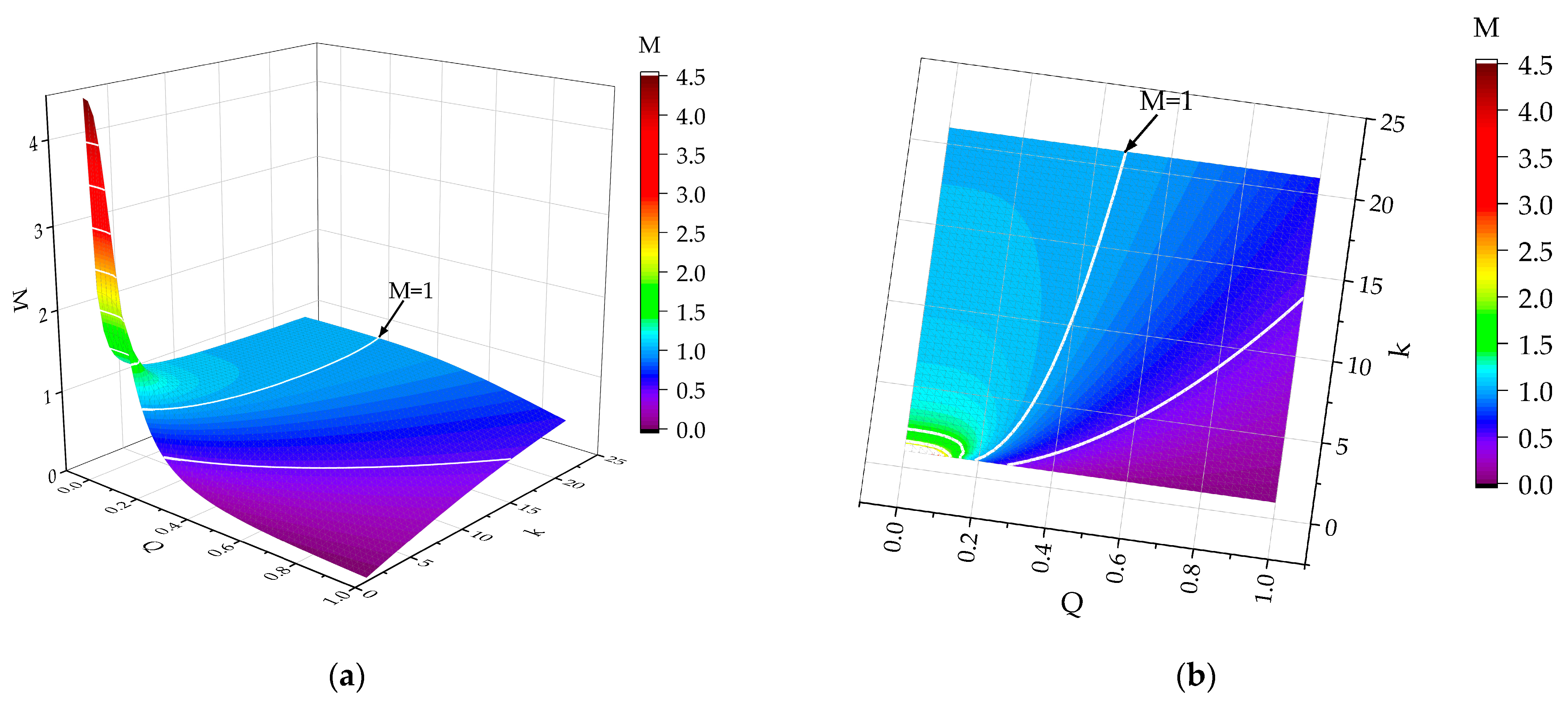
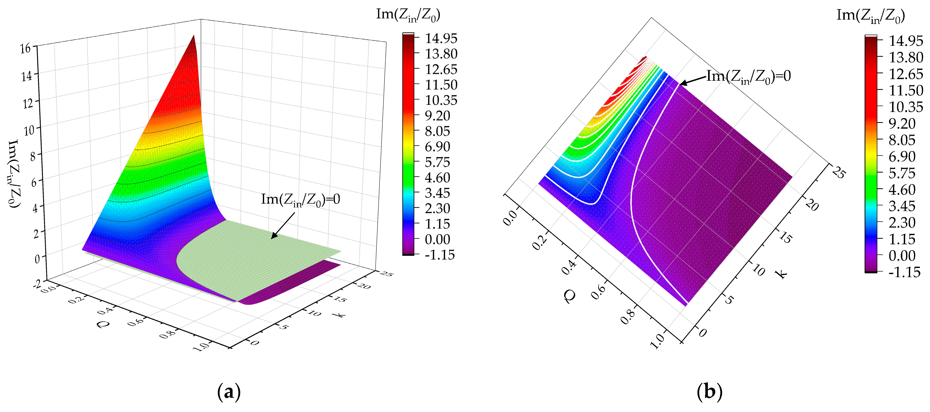
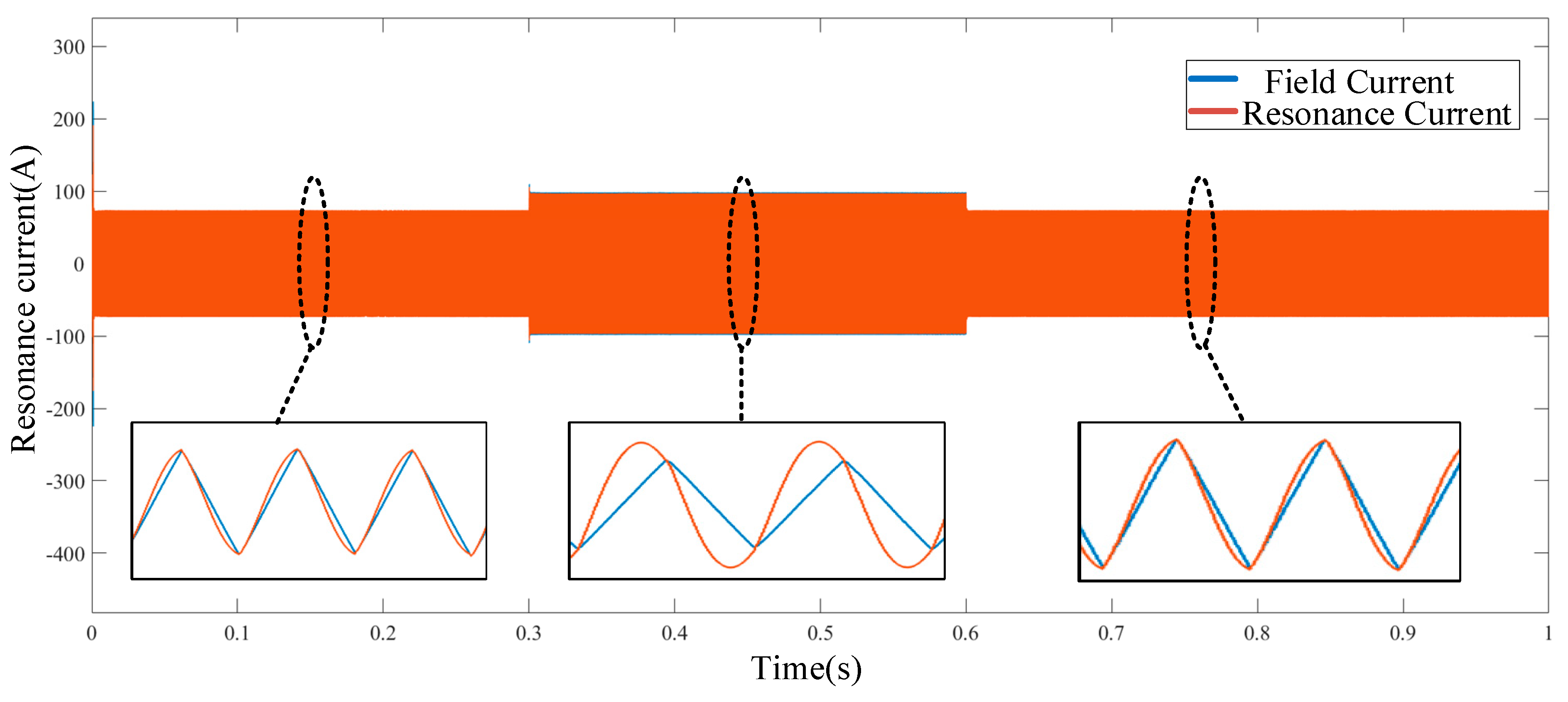
3.2. Characteristic Analysis of CLLLC Resonant Converter
3.3. Design of Converter Parameters
3.3.1. Parameter Design of Buck/Boost Converter
3.3.2. Parameter Design of CLLLLC Resonant Converter
3.3.3. Parameter Design of Transformer
- Selection of magnetic cores
- The number of turns on the original and secondary sides can be calculated
- Selection of wire diameter
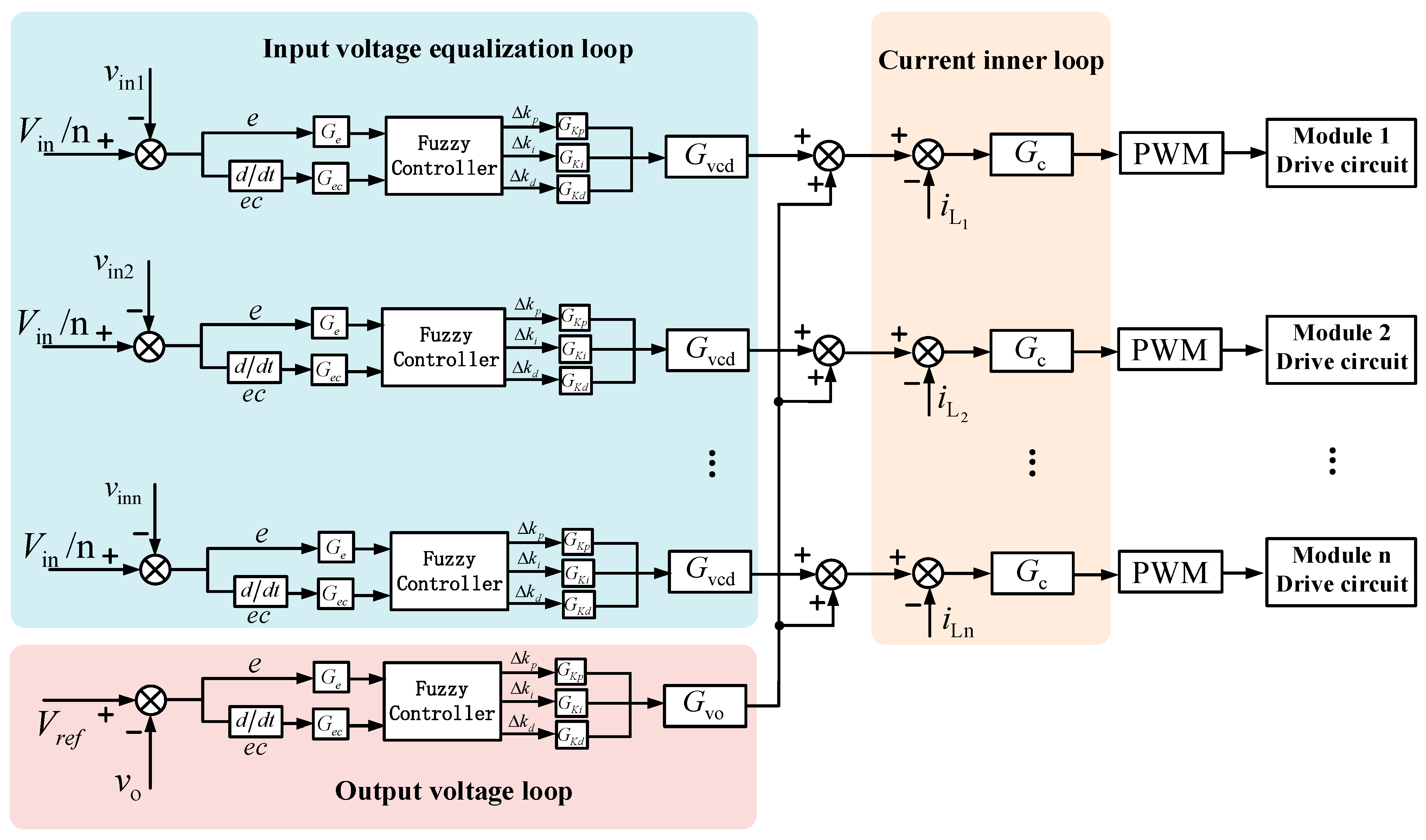
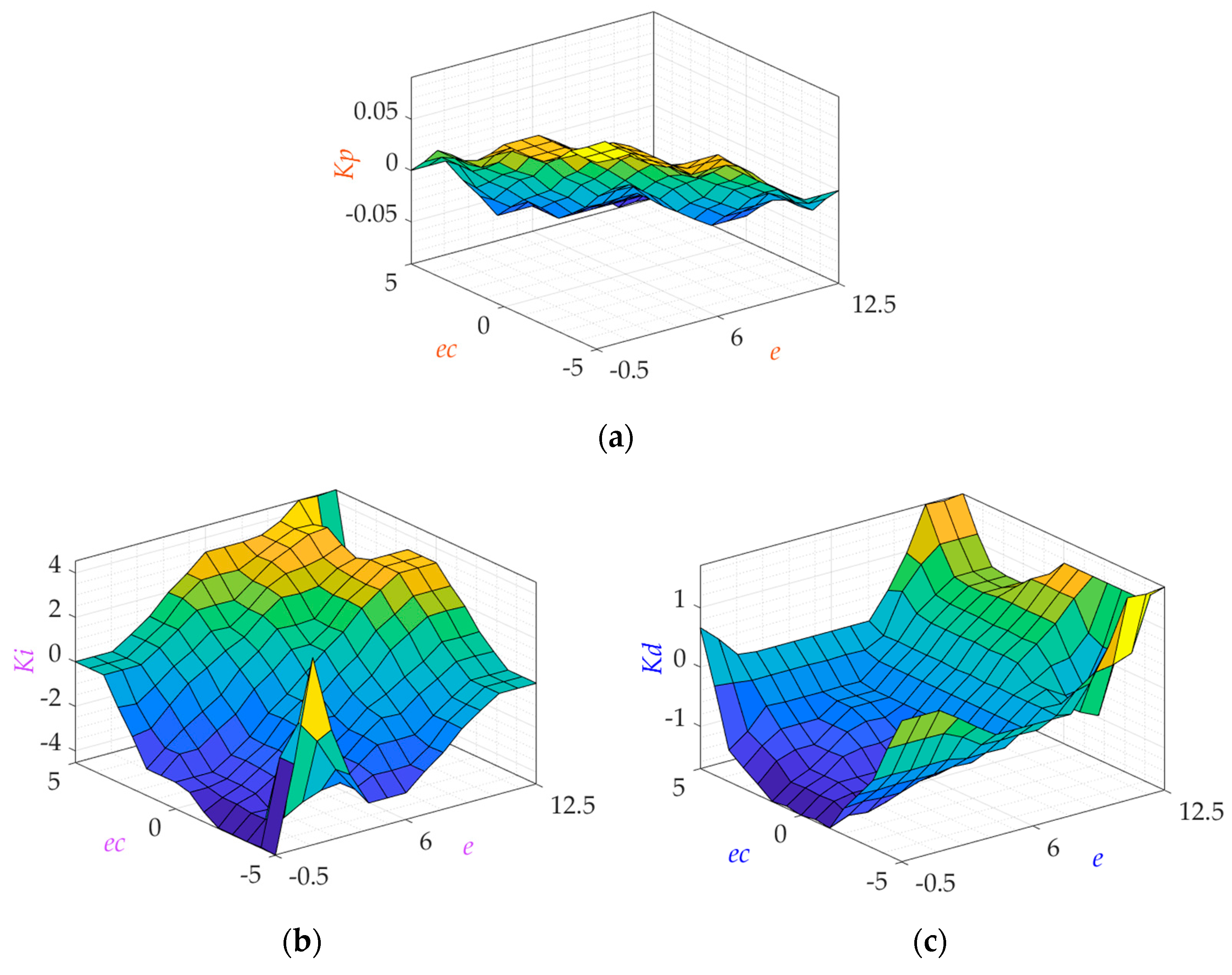
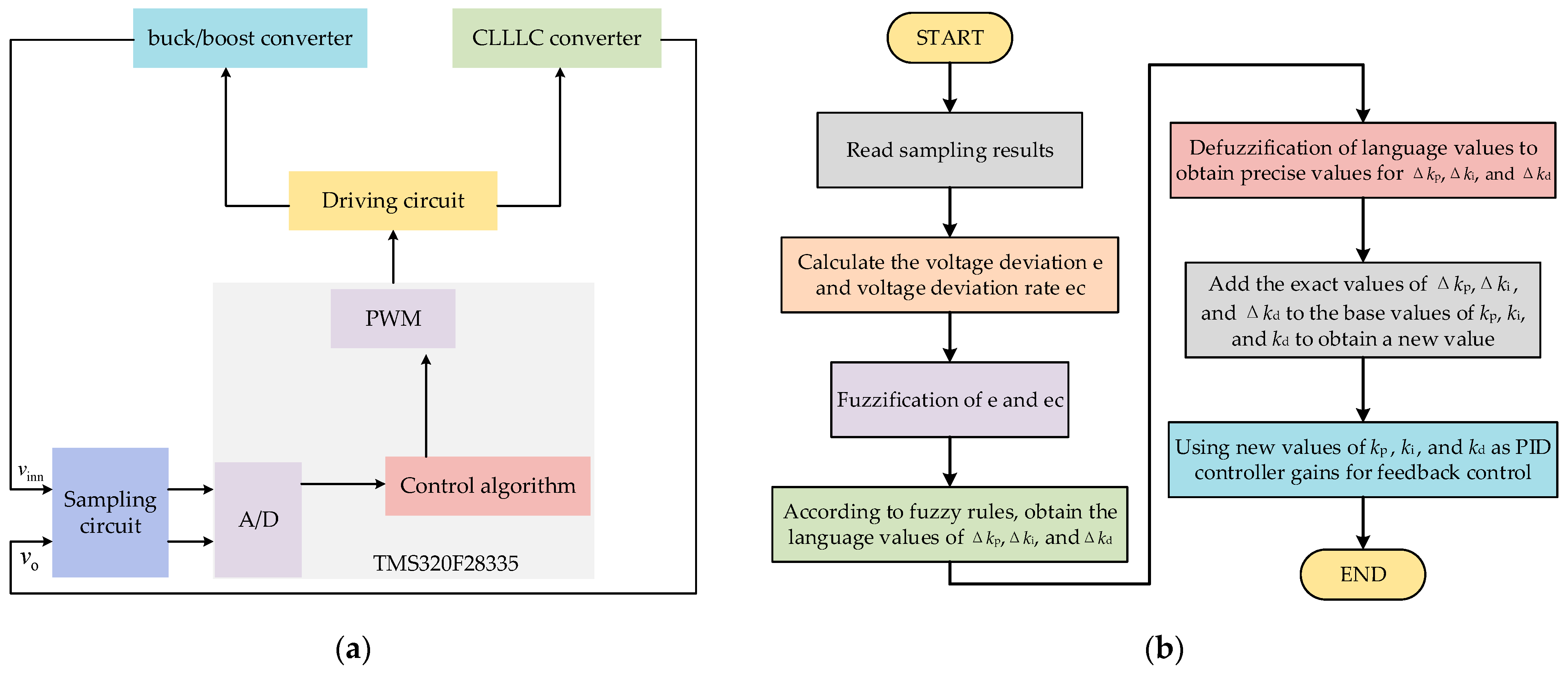
4. Control Strategy of the System
5. Simulation Results and Analysis
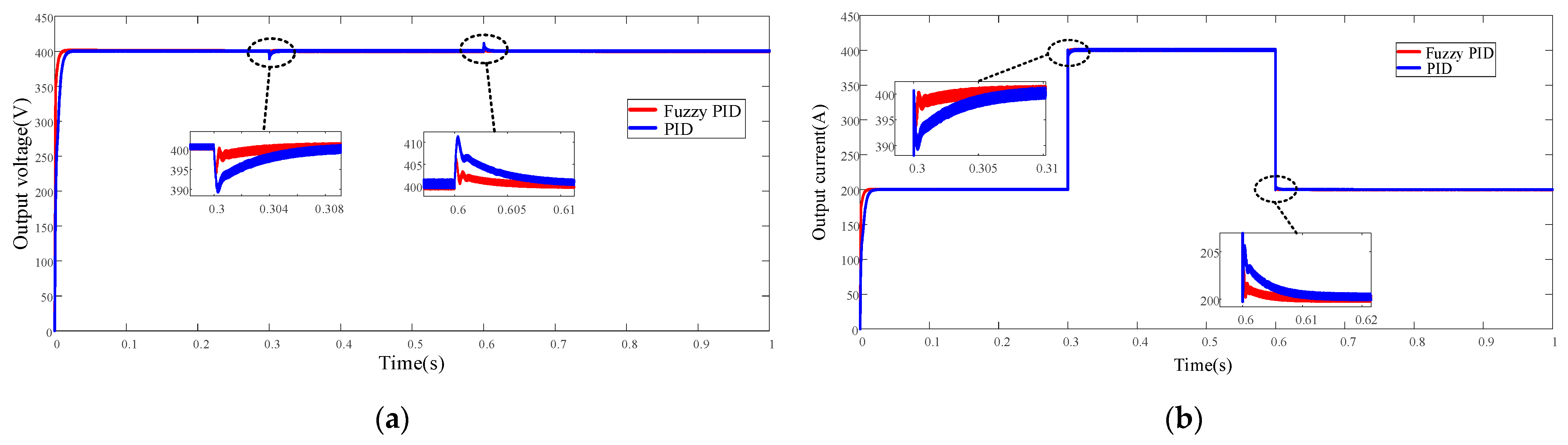
5.1. Load Variation Condition
5.2. Voltage Variation Condition
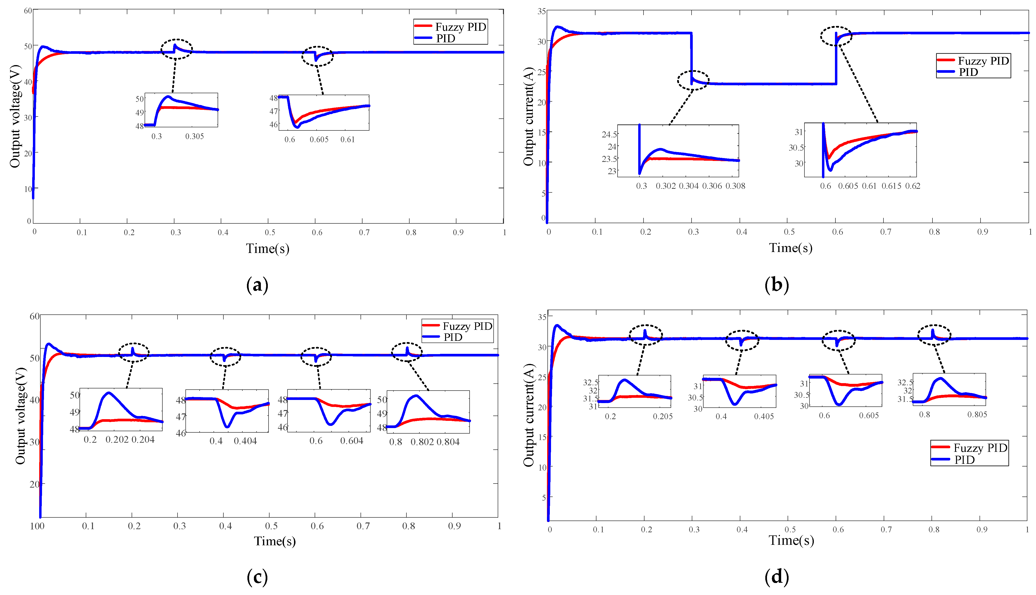
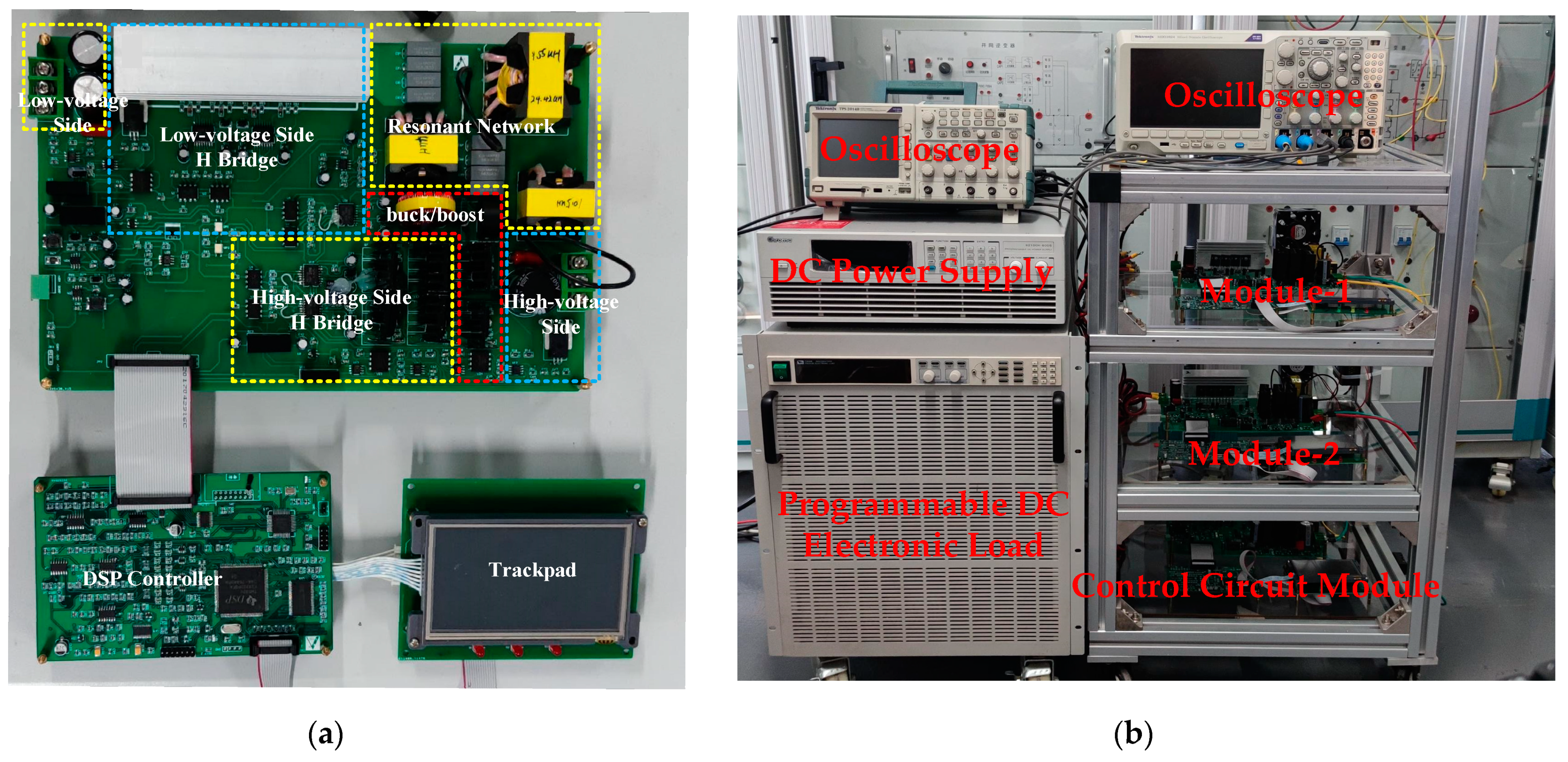
6. Experimental Results and Analysis
6.1. Low-Voltage System Simulation Verification
6.2. Low-Voltage System Experimental Verification
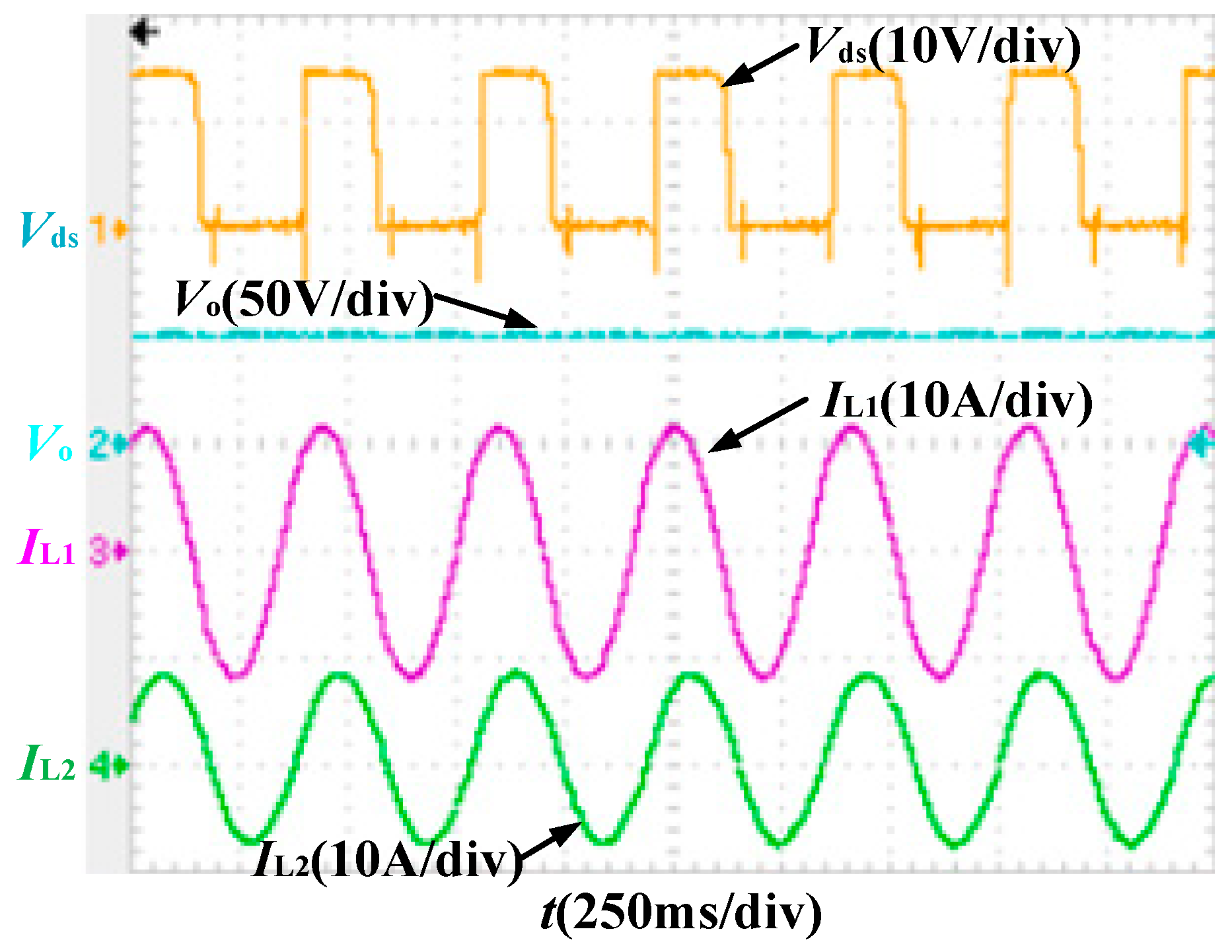
6.2.1. Steady-state Experiment of Submodule
6.2.2. Dynamic Experiment of Submodule
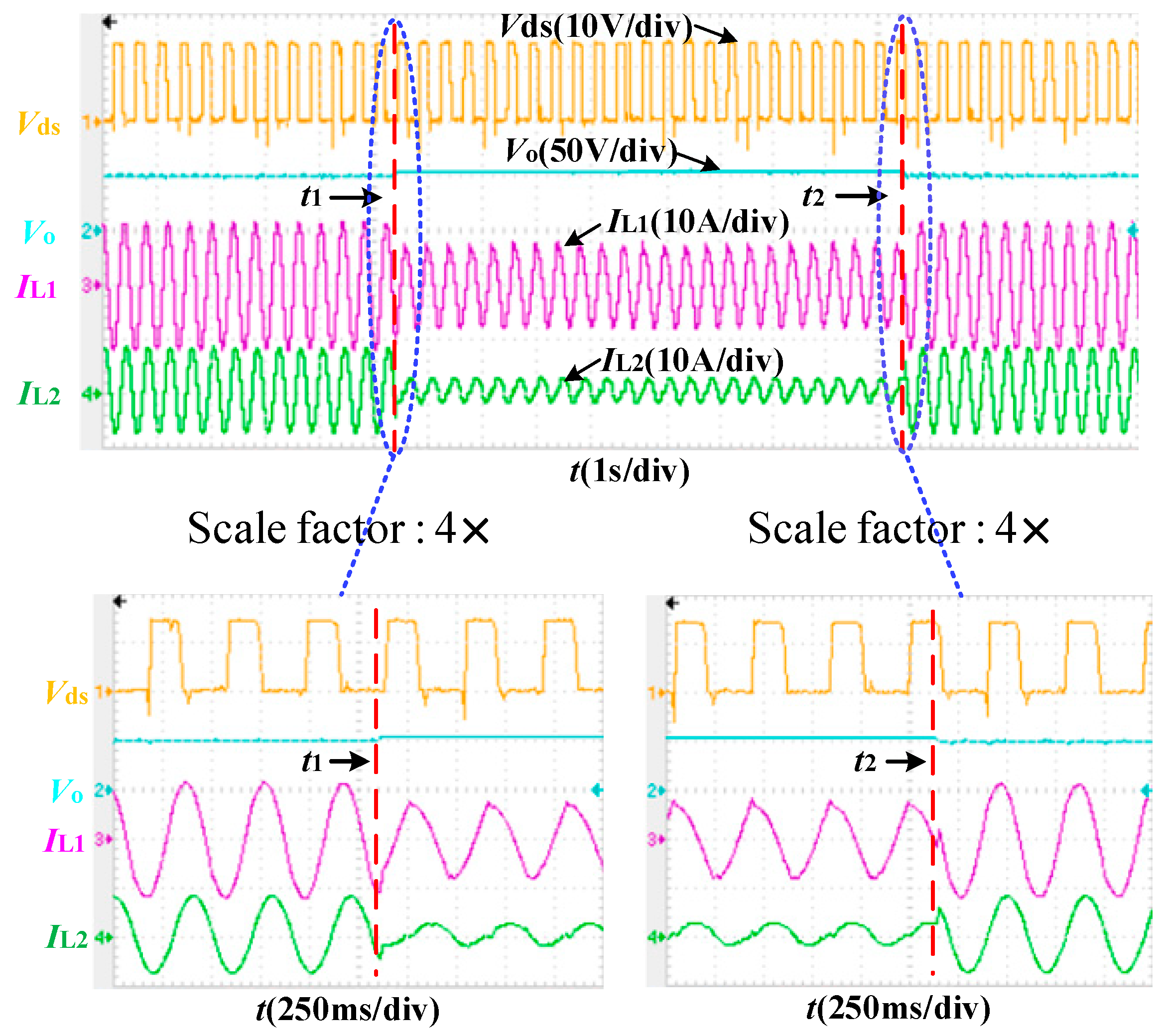
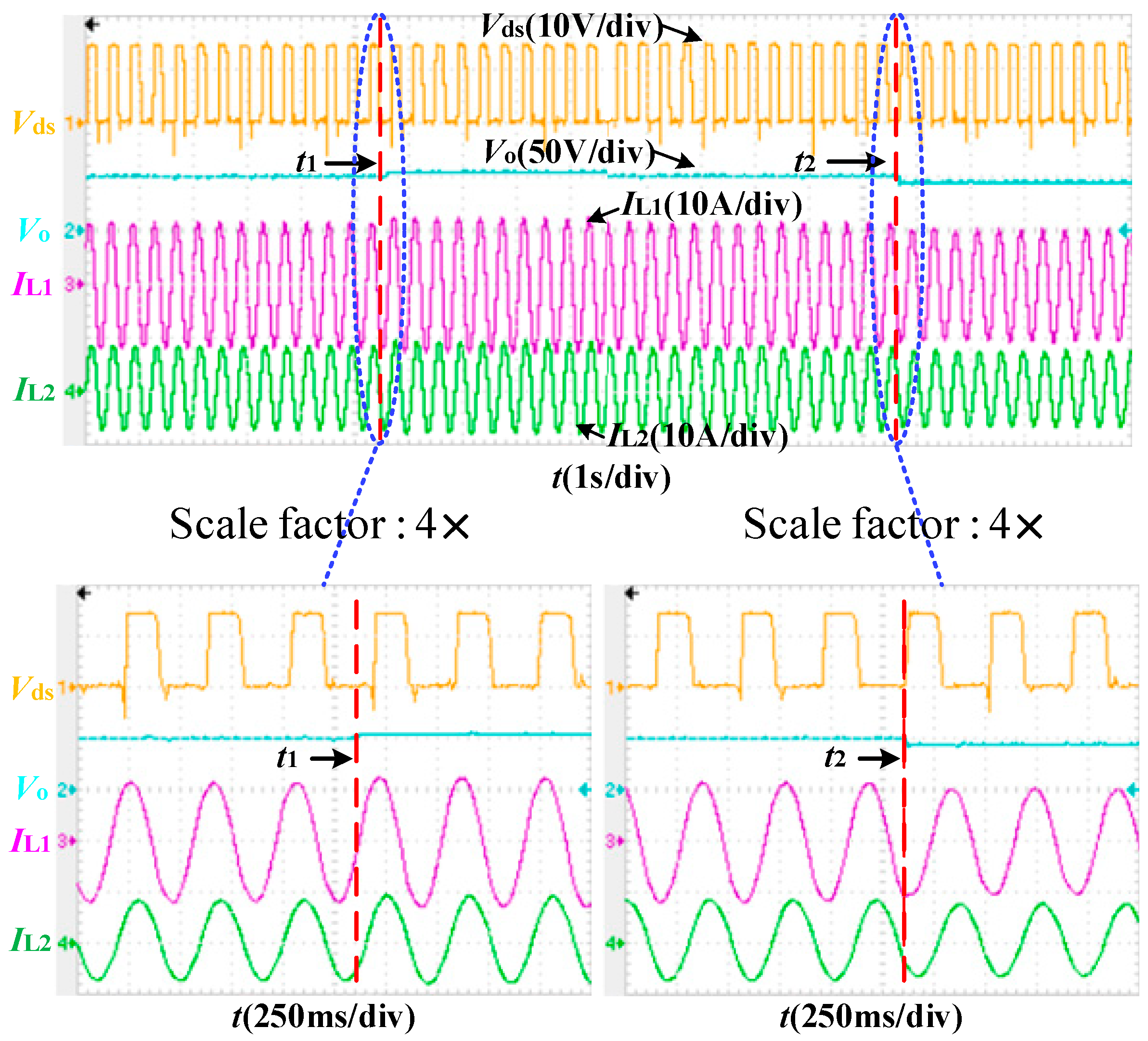
- Load variation condition
- Voltage variation condition
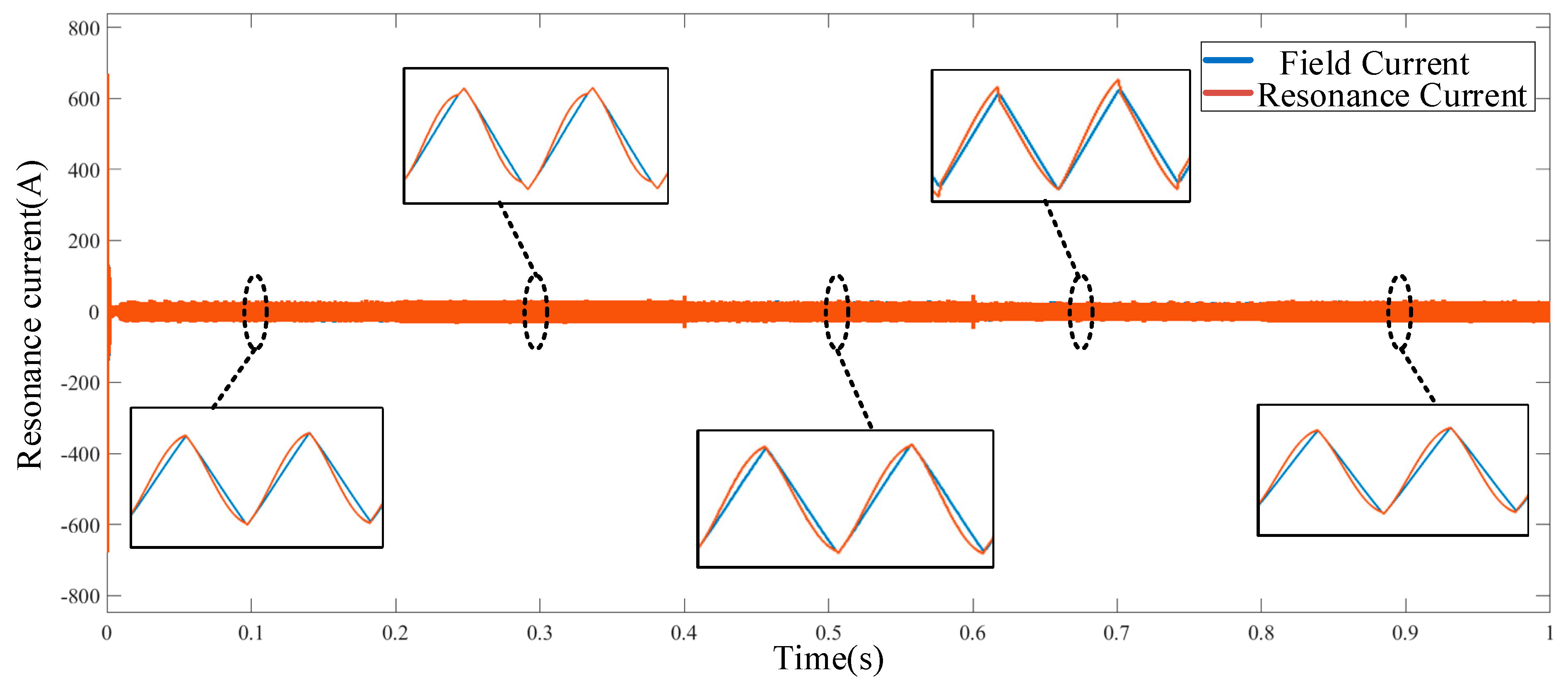
6.2.3. Steady-State Experiment of ISOP System
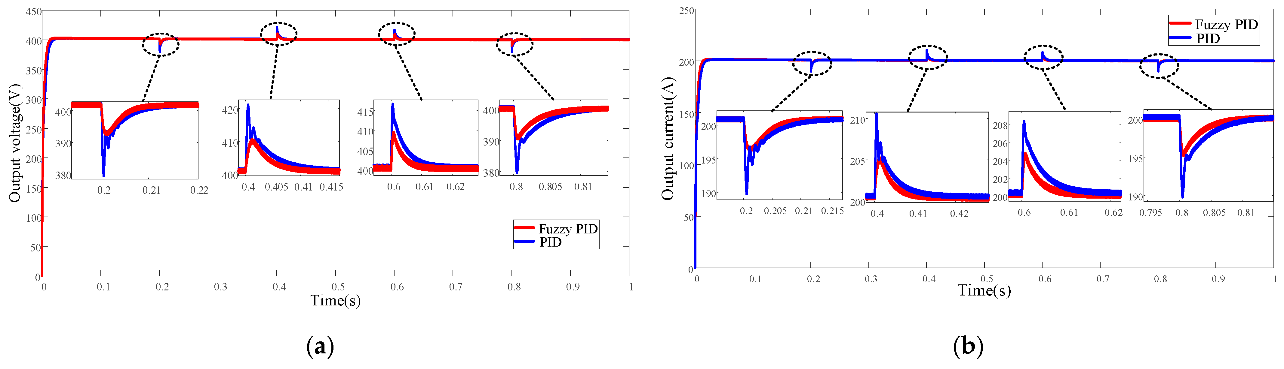
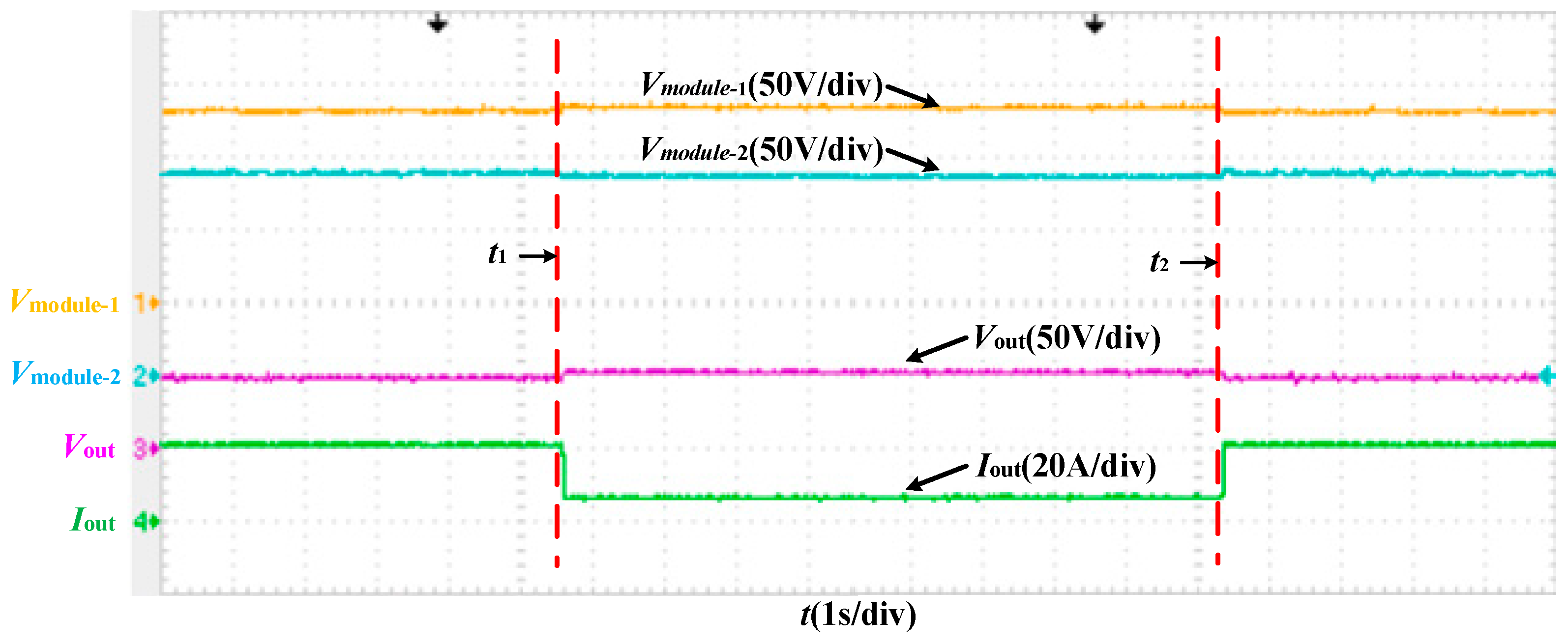
6.2.4. Dynamic Experiment of ISOP System
- Load variation condition
- Voltage variation condition
7. Conclusions
- It is suitable for medium- and high-power applications with a high-voltage input and a low-voltage output, the system is easy to modularize, and can be expanded according to voltage levels;
- The buck/boost converter in the system is used for voltage regulation, while the CLLLC resonant converter plays a role in electrical isolation and voltage matching, and is always near the optimal operating point, resulting in a high conversion efficiency;
- Based on the fuzzy PID three-loop control strategy, the system has a better dynamic performance and stability in the event of voltage or load changes, and can achieve good voltage and current sharing effects.
Author Contributions
Funding
Data Availability Statement
Conflicts of Interest
References
- Lee, M.; Choi, W.; Kim, H.; Cho, B.-H. Operation schemes of interconnected DC microgrids through an isolated bi-directional DC-DC converter. In Proceedings of the 2015 IEEE Applied Power Electronics Conference and Exposition (APEC), Charlotte, NC, USA, 15–19 March 2015; pp. 2940–2945. [Google Scholar]
- Al-Ismail, F.S. DC microgrid planning, operation, and control: A comprehensive review. IEEE Access 2021, 9, 36154–36172. [Google Scholar] [CrossRef]
- Yao, J.; Chen, W.; Xue, C.; Yuan, Y.; Wang, T. An ISOP hybrid DC transformer combining multiple SRCs and DAB converters to interconnect MVDC and LVDC distribution networks. IEEE Trans. Power Electron. 2020, 35, 11442–11452. [Google Scholar] [CrossRef]
- Lan, Z.; Wang, C.; Duan, W.; Yang, Q.; Li, F.; Zhao, Y. Investigation on ISOP DC-DC Converter with SiC-MOSFETs Suitable for DC Distribution Grid. In Proceedings of the 2020 Chinese Automation Congress (CAC), Shanghai, China, 6–8 November 2020; pp. 6340–6343. [Google Scholar]
- Hou, N.; Gunawardena, P.; Wu, X.; Ding, L.; Zhang, Y.; Li, Y.W. An input-oriented power sharing control scheme with fast-dynamic response for ISOP DAB DC–DC converter. IEEE Trans. Power Electron. 2021, 37, 6501–6510. [Google Scholar] [CrossRef]
- Chen, Z.; Zhang, Z.; Sun, X.; Li, Z.; Liu, X. (Eds.) An Optimized Return Power Control for DAB Converter Cluster with ISOP Configuration. In Proceedings of the 2023 IEEE 2nd International Power Electronics and Application Symposium (PEAS), Guangzhou, China, 10–13 November 2023. [Google Scholar]
- Hwang, S.-S.; Baek, S.-W.; Kim, H.-W. Power balance method using coupled shunt inductor and multiple-input transformer for ISOP LLC converter. Electronics 2019, 8, 352. [Google Scholar] [CrossRef]
- Wang, Y.; Chen, C.; Chen, B.; Wang, Z.; Ji, R.; Zhang, M. Transformer integration and winding design for ISOP-LLC converter. In Proceedings of the 2022 IEEE Energy Conversion Congress and Exposition (ECCE), Detroit, MI, USA, 9–13 October 2022; pp. 1–5. [Google Scholar]
- Li, S.; Wang, J.; Li, Y.; Li, H.; Wang, Y.; Zhuo, F.; Wang, F. A Novel ISOP SCDAB-CLLLC Hybrid Bidirectional DC-DC Converter for Renewable Energy DC Grid. In Proceedings of the 2021 IEEE/IAS Industrial and Commercial Power System Asia (I&CPS Asia), Chengdu, China, 18–21 July 2021; pp. 89–94. [Google Scholar]
- Qu, L.; Wang, X.; Zhang, D.; Bai, Z.; Liu, Y. A high efficiency and low shutdown current bidirectional DC-DC CLLLC resonant converter. In Proceedings of the 2019 22nd International Conference on Electrical Machines and Systems (ICEMS), Harbin, China, 11–14 August 2019; pp. 1–6. [Google Scholar]
- Wu, J.; Wang, T.; Shu, Z.; Ma, L.; Wang, S.; Nie, J. Power Balance Control Based on Sensorless Parameters Estimation for ISOP Three-Level DAB Converter. IEEE Trans. Ind. Electron. 2024. [Google Scholar] [CrossRef]
- Chen, W.; Wang, G.; Ruan, X.; Jiang, W.; Gu, W. Wireless Input-Voltage-Sharing Control Strategy for Input-Series Output-Parallel (ISOP) System Based on Positive Output-Voltage Gradient Method. IEEE Trans. Ind. Electron. 2014, 61, 6022–6030. [Google Scholar] [CrossRef]
- Zeng, Y.; Pou, J.; Sun, C.; Mukherjee, S.; Xu, X.; Gupta, A.K.; Dong, J. Autonomous Input Voltage Sharing Control and Triple Phase Shift Modulation Method for ISOP-DAB Converter in DC Microgrid: A Multiagent Deep Reinforcement Learning-Based Method. IEEE Trans. Power Electron. 2023, 38, 2985–3000. [Google Scholar] [CrossRef]
- Chen, X.; Xu, J.; Xu, G. Hybrid SPS Control for ISOP Dual-Active-Bridge Converter Based on Modulated Coupled Inductor with Full Load Range ZVS and RMS Current Optimization in DC Transformer Applications. IEEE Access 2022, 10, 131394–131405. [Google Scholar] [CrossRef]
- Tian, C.; Zhang, J.; Zhou, J.; Zang, J.; Li, Z.; Xi, D.; Wang, F.; Zhang, A.; Liu, L. A multiport embedded DC power flow controller for ISOP-DCT. In Proceedings of the 2021 Annual Meeting of CSEE Study Committee of HVDC and Power Electronics (HVDC 2021), Beijing, China, 28–30 December 2021; pp. 163–169. [Google Scholar]
- Li, S.; Wang, Z.; Zhang, Y.; Sun, L.; Wang, K.; Wu, X.; Yuan, X. Hardware Design and Decoupled Three-Loop Control for a 10kV/400V ISOP-DAB Converter. In Proceedings of the 2023 11th International Conference on Power Electronics and ECCE Asia (ICPE 2023–ECCE Asia), Jeju Island, Republic of Korea, 22–25 May 2023; pp. 2018–2025. [Google Scholar]
- Wang, M.; Pan, S.; Gong, J.; Lin, W.; Zha, X. (Eds.) A Digital Adaptive Voltage Positioning Technique for 48-1V ISOP-LLC Converter based on Bang-Bang Charge Control. In Proceedings of the 2021 IEEE Applied Power Electronics Conference and Exposition (APEC), Phoenix, AZ, USA, 14–17 June 2021. [Google Scholar]
- Wang, Y.; Sun, Z.; Wu, Q.; Wang, Q.; Xiao, L. A Sensorless Input Voltage Sharing Control for ISOP DAB Converters. In Proceedings of the 2021 IEEE 1st International Power Electronics and Application Symposium (PEAS), Shanghai, China, 13–15 November 2021; pp. 1–4. [Google Scholar]
- Kim, S.H.; Kim, B.J.; Won, C.Y. A Study on Decentralized Inverse-Droop Control for Input Voltage Sharing of ISOP Converter in the Current Control Loop. In Proceedings of the 2019 10th International Conference on Power Electronics and ECCE Asia (ICPE 2019–ECCE Asia), Busan, Republic of Korea, 27–30 May 2019; pp. 2382–2387. [Google Scholar]
- Shi, C.; Ding, Z. Decoupling Control Strategy of DC Power Supply System Combining 24-pulse Rectifier and ISOP-DAB. In Proceedings of the 2022 IEEE International Conference on Power Systems and Electrical Technology (PSET), Aalborg, Denmark, 13–15 October 2022; pp. 359–364. [Google Scholar]
- Liu, H.; Cui, S.; Liu, C.; Sun, H. Small-signal Modeling and Input Impedance of ISOP DC Transformer with Switched Resonant Branches for Self-Voltage Balancing. In Proceedings of the 2022 IEEE 5th International Electrical and Energy Conference (CIEEC), Nanjing, China, 27–29 May 2022; pp. 2818–2823. [Google Scholar]
- Serban, E.; Pondiche, C.; Ordonez, M. Analysis and Design of Bidirectional Parallel-Series DAB-Based Converter. IEEE Trans. Power Electron. 2023, 38, 10370–10382. [Google Scholar] [CrossRef]
- Liu, J.; Zhang, J.; Zheng, T.Q.; Yang, J. A Modified Gain Model and the Corresponding Design Method for an LLC Resonant Converter. IEEE Trans. Power Electron. 2017, 32, 6716–6727. [Google Scholar] [CrossRef]
- Hu, H.; Fang, X.; Chen, F.; Shen, Z.J.; Batarseh, I. A Modified High-Efficiency LLC Converter with Two Transformers for Wide Input-Voltage Range Applications. IEEE Trans. Power Electron. 2013, 28, 1946–1960. [Google Scholar] [CrossRef]
- Jin, N.-Z.; Feng, Y.; Chen, Z.-Y.; Wu, X.-G. Bidirectional CLLLC Resonant Converter Based on Frequency-Conversion and Phase-Shift Hybrid Control. Electronics 2023, 12, 1605. [Google Scholar] [CrossRef]
- Zhou, K.; Sun, Y. Research on Bidirectional Isolated Charging System Based on Resonant Converter. Electronics 2022, 11, 3625. [Google Scholar] [CrossRef]
- Chao, C.-T.; Sutarna, N.; Chiou, J.-S.; Wang, C.-J. An Optimal Fuzzy PID Controller Design Based on Conventional PID Control and Nonlinear Factors. Appl. Sci. 2019, 9, 1224. [Google Scholar] [CrossRef]
- Wang, Y.; Zou, H.; Tao, J.; Zhang, R. Predictive fuzzy PID control for temperature model of a heating furnace. In Proceedings of the 2017 36th Chinese Control Conference (CCC), Dalian, China, 26–28 July 2017; pp. 4523–4527. [Google Scholar]
- Sun, L.; Ma, J.; Yang, B. Fuzzy PID Design of Vehicle Attitude Control Systems. In Proceedings of the 2020 Chinese Control and Decision Conference (CCDC), Hefei, China, 22–24 August 2020; pp. 1826–1830. [Google Scholar]
- Muhammad, Z.; Dziauddin, S.H.A.; Hamid, S.A.; Leh, N.A.M. Water Level Control in Boiler System Using Self-tuning Fuzzy PID Controller. In Proceedings of the 2023 IEEE 13th International Conference on Control System, Computing and Engineering (ICCSCE), Penang, Malaysia, 25–26 August 2023; pp. 232–237. [Google Scholar]


| Parameter | Symbol | Value |
|---|---|---|
| buck/boost rated input voltage | Vin-rated | 3333 V |
| buck/boost input voltage range | Vin | 3000–3666 V |
| buck/boost output resistance | R | 20 Ω |
| buck/boost switch frequency | fs1 | 20 kHz |
| Voltage ripple | ΔV | <0.2% |
| CLLLC rated input voltage | VCLLLC-rated | 1200 V |
| CLLLC input voltage range | VCLLLC | 1147–1253 V |
| CLLLC rated output voltage | Vo-rated | 400 V |
| CLLLC output voltage range | Vo | 390–410 V |
| CLLLC output resistor | Ro | 2 Ω |
| CLLLC switching frequency | fs2 | 75–131 kHz |
| Resonant frequency | fr | 100 kHz |
| Δkp | e | |||||||
|---|---|---|---|---|---|---|---|---|
| NB | NM | NS | Z | PS | PM | PB | ||
| ec | NB | PB | PB | PM | PM | PS | Z | Z |
| NM | PB | PB | PM | PS | PS | Z | NS | |
| NS | PM | PM | PM | PS | Z | NS | NS | |
| Z | PM | PM | PS | Z | NS | NM | NM | |
| PS | PS | PS | Z | NS | NS | NM | NM | |
| PM | PS | Z | NS | NM | NM | NM | NB | |
| PB | Z | Z | NM | NM | NM | NB | NB | |
| Δki | e | |||||||
|---|---|---|---|---|---|---|---|---|
| NB | NM | NS | Z | PS | PM | PB | ||
| ec | NB | NB | NB | NM | NM | NS | Z | Z |
| NM | NB | NB | NM | NS | NS | Z | Z | |
| NS | NB | NM | NS | NS | Z | PS | PS | |
| Z | NM | NM | NS | Z | PS | PM | PM | |
| PS | NM | NS | Z | PS | PS | PM | PB | |
| PM | Z | Z | PS | PS | PM | PB | PB | |
| PB | Z | Z | PS | PM | PM | PB | PB | |
| Δkd | e | |||||||
|---|---|---|---|---|---|---|---|---|
| NB | NM | NS | Z | PS | PM | PB | ||
| ec | NB | PS | NS | NB | NB | NB | NM | PS |
| NM | PS | NS | NB | NM | NM | NS | Z | |
| NS | Z | NS | NM | NM | NS | NS | Z | |
| Z | Z | NS | NS | NS | NS | NS | Z | |
| PS | Z | Z | Z | Z | Z | Z | Z | |
| PM | PB | NS | PS | PS | PS | PS | PB | |
| PB | PB | PM | PM | PM | PS | PS | PB | |
| Converter | Symbol | Parameter | Value |
|---|---|---|---|
| buck/boost | LB | Energy storage inductor | 0.4 mH |
| C1 | Input side capacitance | 700 μF | |
| C2 | Output side capacitance | 250 μF | |
| fs1 | Switching frequency | 20 kHz | |
| CLLLC | L1 | Resonant inductance | 1.86 μH |
| L2 | Resonant inductance | 0.827 μH | |
| C3 | Resonant capacitor | 1363 nF | |
| C4 | Resonant capacitor | 3066.75 nF | |
| Lm | Magnetizing inductance | 9.3 μH | |
| n | Transformer ratio | 3 | |
| fs2 | Switching frequency | 100 kHz |
Disclaimer/Publisher’s Note: The statements, opinions and data contained in all publications are solely those of the individual author(s) and contributor(s) and not of MDPI and/or the editor(s). MDPI and/or the editor(s) disclaim responsibility for any injury to people or property resulting from any ideas, methods, instructions or products referred to in the content. |
© 2024 by the authors. Licensee MDPI, Basel, Switzerland. This article is an open access article distributed under the terms and conditions of the Creative Commons Attribution (CC BY) license (https://creativecommons.org/licenses/by/4.0/).
Share and Cite
Wen, C.; Li, S.; Wang, P.; Li, J. An Input-Series Output-Parallel DC–DC Converter Based on Fuzzy PID Three-Loop Control Strategy. Electronics 2024, 13, 2342. https://doi.org/10.3390/electronics13122342
Wen C, Li S, Wang P, Li J. An Input-Series Output-Parallel DC–DC Converter Based on Fuzzy PID Three-Loop Control Strategy. Electronics. 2024; 13(12):2342. https://doi.org/10.3390/electronics13122342
Chicago/Turabian StyleWen, Chunxue, Shuhui Li, Peng Wang, and Jianlin Li. 2024. "An Input-Series Output-Parallel DC–DC Converter Based on Fuzzy PID Three-Loop Control Strategy" Electronics 13, no. 12: 2342. https://doi.org/10.3390/electronics13122342
APA StyleWen, C., Li, S., Wang, P., & Li, J. (2024). An Input-Series Output-Parallel DC–DC Converter Based on Fuzzy PID Three-Loop Control Strategy. Electronics, 13(12), 2342. https://doi.org/10.3390/electronics13122342