Article

Effects of Current Filaments on IGBT Avalanche Robustness: A Simulation Study

1
Key Laboratory of Optoelectronic Technology & Systems, Chongqing University, Chongqing 400044, China
2
Key Laboratory of Power Transmission Equipment & System Security and New Technology, Chongqing University, Chongqing 400044, China
3
Faculty of EEMCS, Delft University of Technology, Mekelweg 4, 2628 CD Delft, The Netherlands
*
Author to whom correspondence should be addressed.
Electronics 2024, 13(12), 2347; https://doi.org/10.3390/electronics13122347
Submission received: 8 May 2024 / Revised: 7 June 2024 / Accepted: 13 June 2024 / Published: 15 June 2024
(This article belongs to the Section Power Electronics)

Abstract

:
With the increase in voltage level and current capacity of the insulated gate bipolar transistor (IGBT), the avalanche effect has become an important factor limiting the safe operating area (SOA) of the device. The hole injection into the p/n junction on the backside of the IGBT after avalanche is the main feature that distinguishes the avalanche effect from other devices. In this paper, the avalanche breakdown characteristics of IGBT and the nature of current filament are investigated using theoretical analysis and numerical simulation, and the underlying physical mechanism controlling the nature of current filaments is revealed. The results show that the hole injection on the backside of the IGBT leads to an additional negative differential resistance (NDR) branch on the avalanche breakdown curve. The device’s common-base current gain, αpnp, is a crucial factor in determining the current filament. As αpnp increases, the avalanche-induced current filament becomes stronger and slower, resulting in weaker avalanche robustness of the device.

1. Introduction

The avalanche multiplication effect occurs when the voltage applied across the power device exceeds the maximum blocking voltage it can withstand, resulting in avalanche breakdown. Generally, researchers focus more on the magnitude of avalanche breakdown voltage and strategies to increase this voltage. However, the characteristics exhibited by the device after avalanche breakdown are essential due to their direct impact on the device’s stability under overvoltage conditions [1,2,3]. Many studies have shown that when the device operates in the negative differential resistance (NDR) region of the avalanche breakdown curve, a localized aggregation of currents (current filaments) induced by the avalanche effect occurs within the device [4,5,6,7]. The concentration effect of avalanche current leads to the gathering of avalanche energy at the location of the current filament, significantly reducing the device’s robustness to avalanche breakdown and possibly leading to device failure [8,9,10,11,12]. When avalanche breakdown occurs in a device due to significant power dissipation, it is generally not feasible to test it directly through experiments. Therefore, research on avalanche breakdown characteristics mainly relies on device simulation and theoretical analysis methods.
In 1966, Egawa et al. first discovered the negative differential resistance effect following the avalanche breakdown of a high-voltage power diode [13]. A more in-depth and systematic description of this physical effect was provided by Lutz et al. in 2009 [14]. When avalanche breakdown occurs in a diode and the avalanche current is high, the avalanche breakdown curve will show a strong NDR branch due to the formation of a hammock-like Egawa electric field distribution inside the device. Consequently, when the device operates on the NDR branch, the NDR effect can cause current aggregation within the device, forming current filaments and making the device highly susceptible to failure [13,14,15]. For power metal oxide semiconductor field effect transistors (MOSFETs), the avalanche breakdown characteristics are similar to those of diodes due to their similar blocking mechanism [16,17,18].
In 2014, Spirito et al. investigated the avalanche breakdown characteristics of a 1.2 kV planar gate IGBT [19]. The avalanche breakdown curve of the IGBT shows two NDR branches: one at a higher avalanche current with a formation mechanism similar to that of a diode, both influenced by the Egawa electric field distribution, and another at a lower current due to hole injection on its backside, distinguishing the IGBT from diodes and power MOSFETs. Although the unique NDR branch on the avalanche breakdown curve of the IGBT is the primary cause of the induced current filaments and its formation mechanism has been revealed, previous studies have not established a clear link between the NDR effect and the nature of the current filaments. Accordingly, the lack of a control mechanism for the NDR effect on these filaments limits our complete understanding of the factors affecting the robustness of IGBTs during avalanche.
In this paper, we investigate the avalanche robustness of the 650 V trench field-stop IGBT (FS-IGBT) through theoretical analysis and Sentaurus TCAD numerical simulations. First, we investigate the avalanche breakdown characteristics of IGBTs using static simulation, including the formation mechanism of the negative differential resistance branch on the avalanche breakdown curve and the effects of critical structural parameters αpnp and temperature on these characteristics. Then, by dynamically simulating the device operating in the NDR branch of its avalanche breakdown curve, we comparatively analyze the nature of the device’s internal current filaments under constant temperature, electrothermal coupling, and various structural parameters. Finally, we reveal the control mechanism of the NDR effect on the current filament and its impact on the device’s robustness by integrating the avalanche breakdown characteristics with static simulations.

2. Avalanche Breakdown Characteristics of FS-IGBT

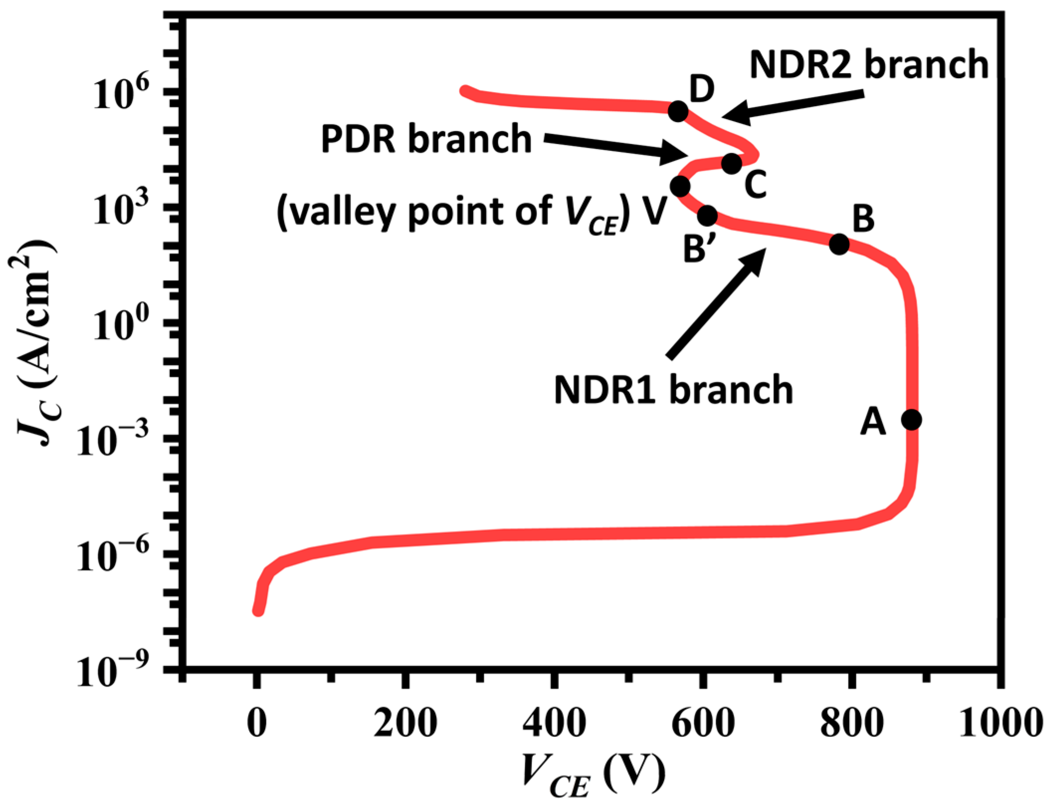
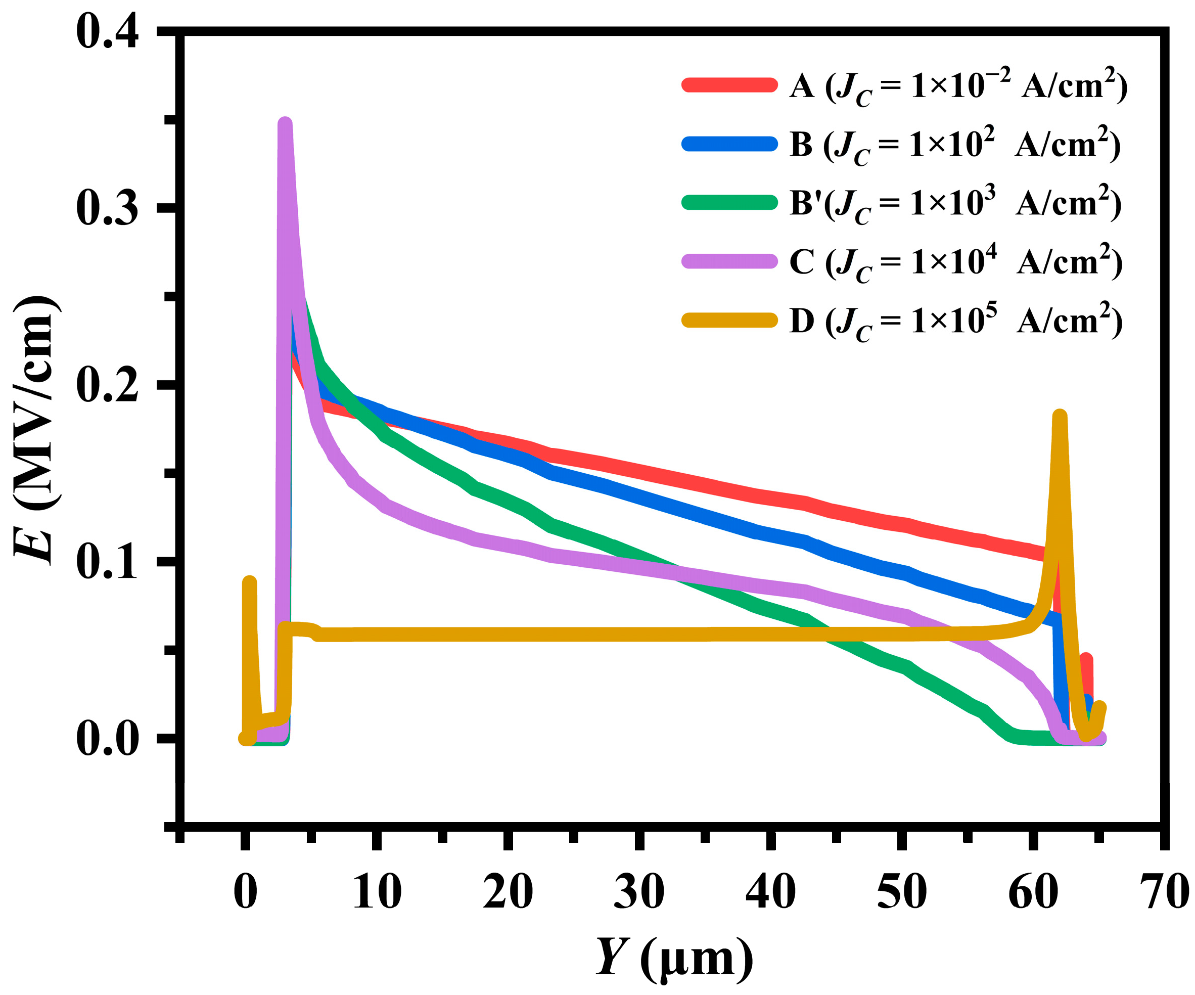
2.1. Mechanism of Negative Differential Resistance Branching

Figure 1 shows the cell structure of 650 V trench FS-IGBT. Specifically, the three p/n junctions of the FS-IGBT are labeled J1, J2, and J3. The N-drift region, with a doping concentration of 1 × 1014 cm−3 and a thickness of 62 μm, is designed to withstand a breakdown voltage exceeding 650 V. Additionally, the gate oxide has a thickness of 0.12 μm, while the gate trench measures 5 μm in depth and 1 μm in width. The other parameters are listed in Table 1.
The blocking behavior of the FS-IGBT can be equated to that of a PNP transistor with an open base. As shown in Figure 2, when avalanche breakdown occurs and the avalanche current increases, the first NDR branch (NDR1 branch) emerges on the avalanche breakdown curve. This is followed by the appearance of a Positive Differential Resistance (PDR) branch. Finally, the second NDR branch (NDR2 branch) appears.
To investigate the formation mechanism of different differential resistance branches on the avalanche breakdown curve of FS-IGBT, the electric field distribution inside the device on each branch is analyzed, as shown in Figure 3. Concretely, the integration of the electric field over vertical distance represents the voltage applied to the device.
When the device operates at point A on the avalanche breakdown curve in Figure 2, the internal electric field is almost linearly distributed in the N drift region, as the avalanche current is minimal at this time. There are few mobile carriers in the space charge region, fewer than the background doping concentration of the device. According to the Poisson equation, the electric field gradient in the N drift region is determined solely by the doping concentration ND, as described by the following equation [20]:
d E d y = q ε S i N D
where q represents the elementary charge, and εSi is the dielectric constant of silicon.
As the avalanche current increases, the NDR1 branch appears and the area enclosed by the electric field decreases. As shown at points B and B′ in Figure 3, the area enclosed by the electric field decreases because the electric field gradient increases. This occurs as electrons generated by the avalanche near junction J2 move to the collector side. This movement is equivalent to supplying a base current to a PNP transistor with an open base, thus inducing hole injection from the collector region through the positively-biased junction J1 to the N drift region. According to Poisson’s equation, the electric field gradient at this point is no longer determined by Equation (1) but by the following equation [14]:
d E d y = q ε S i ( N D + p + p a v n a v )
where pav and nav are the densities of holes and electrons generated by avalanches in the space charge region, respectively, and p is the density of holes injected into junction J1. The magnitude of p is determined by the αpnp at this time, as described by the following equation [3,21]:
α p n p = γ p α T 1 = γ p 1 cosh ( W F S L p , e f f )
where αpnp is the standard base current gain of the PNP transistor, γp is the hole injection efficiency of the junction J1, αT1 is the transport coefficient of the undepleted part of the FS layer, WFS is the thickness of the undepleted part of the FS layer, and Lp,eff is the effective diffusion length of the holes in the FS layer.
As JC increases, the density of holes injected into the FS layer also increases, surpassing the background doping concentration of the FS layer. Consequently, the FS layer shifts from a low-level to a high-level injection state, leading to an increase in Lp,eff, which is limited by the bipolar diffusion coefficient La,FS in the FS layer. As a result, the αpnp increases during this process, resulting in a decrease in VCE. Meanwhile, according to Equation (3), the high hole density p injected into the N- region is large enough to affect the ND, causing the electric field gradient to steepen, thereby reducing the surrounding area and VCE.
As JC continues to increase, the avalanche effect at junction J2 becomes stronger. More electrons are generated by the avalanche, which increases the base current of the PNP transistor and results in more holes being injected into the N drift region. Therefore, the electric field gradient at point B’ is steeper than that at point B, resulting in a smaller VCE at point B’, and hence the formation of the NDR1 branch. This branch is a critical feature that distinguishes the avalanche characteristics of FS-IGBT from those of the power diode, primarily because there is no P+ region and no hole injection on the backside of the diode.
As the avalanche current continues to increase, VCE decreases to a minimum value, such as point V in Figure 2, and then begins to increase, forming a PDR branch. From the electric field distribution at point C in Figure 3, it is apparent that the electric field warps upward on the collector side due to a significantly slower electric field gradient, thereby increasing the area surrounded by the electric field. This indicates a decrease in the holes injected into the N-drift region, leading to a reduction in αpnp. As shown in Equation (3), although JC places the FS layer in a high-level injection state, the electrons in this state will diffuse back into the collector region. This results in a significant reduction in the hole injection efficiency, γp, at junction J1, which sharply decreases αpnp. The reduction in αpnp leads to an increase in VCE, thus forming the PDR branch. The formation mechanism of this branch in the FS-IGBT is similar to that of the PDR branch in the diode, attributed to the warping of the electric field near the backside high-low junctions.
With a further increase in JC, the FS-IGBT transitions from the PDR branch to the NDR2 branch. This transition is attributed to the occurrence of the Egawa electric field, which produces a high electric field at both ends of the device, creating a mutually reinforcing bilateral avalanche effect. This effect is illustrated in the electric field distribution at point D in Figure 3 [16,22]. This branch forms through the same mechanism as the NDR branch in the power diode.

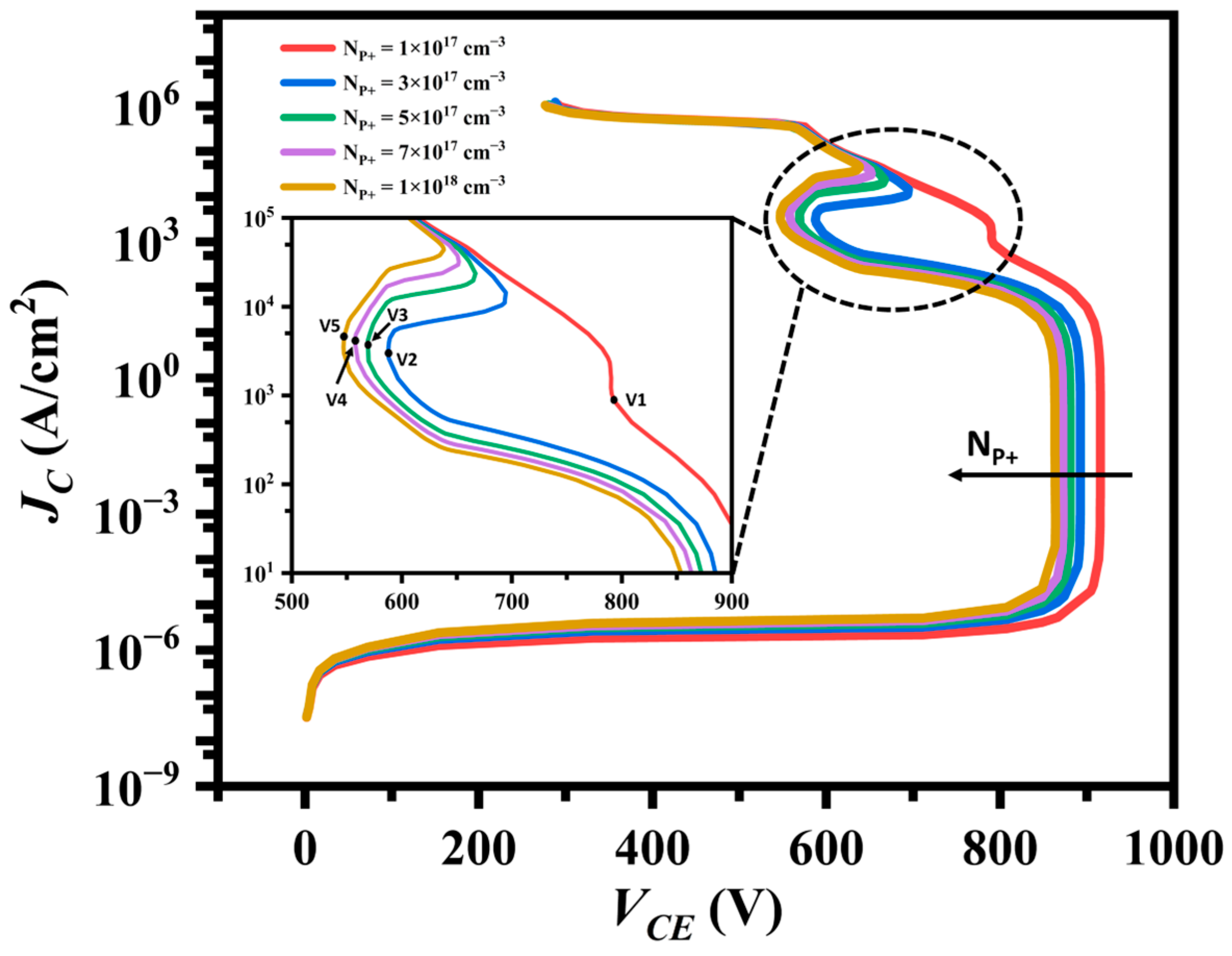
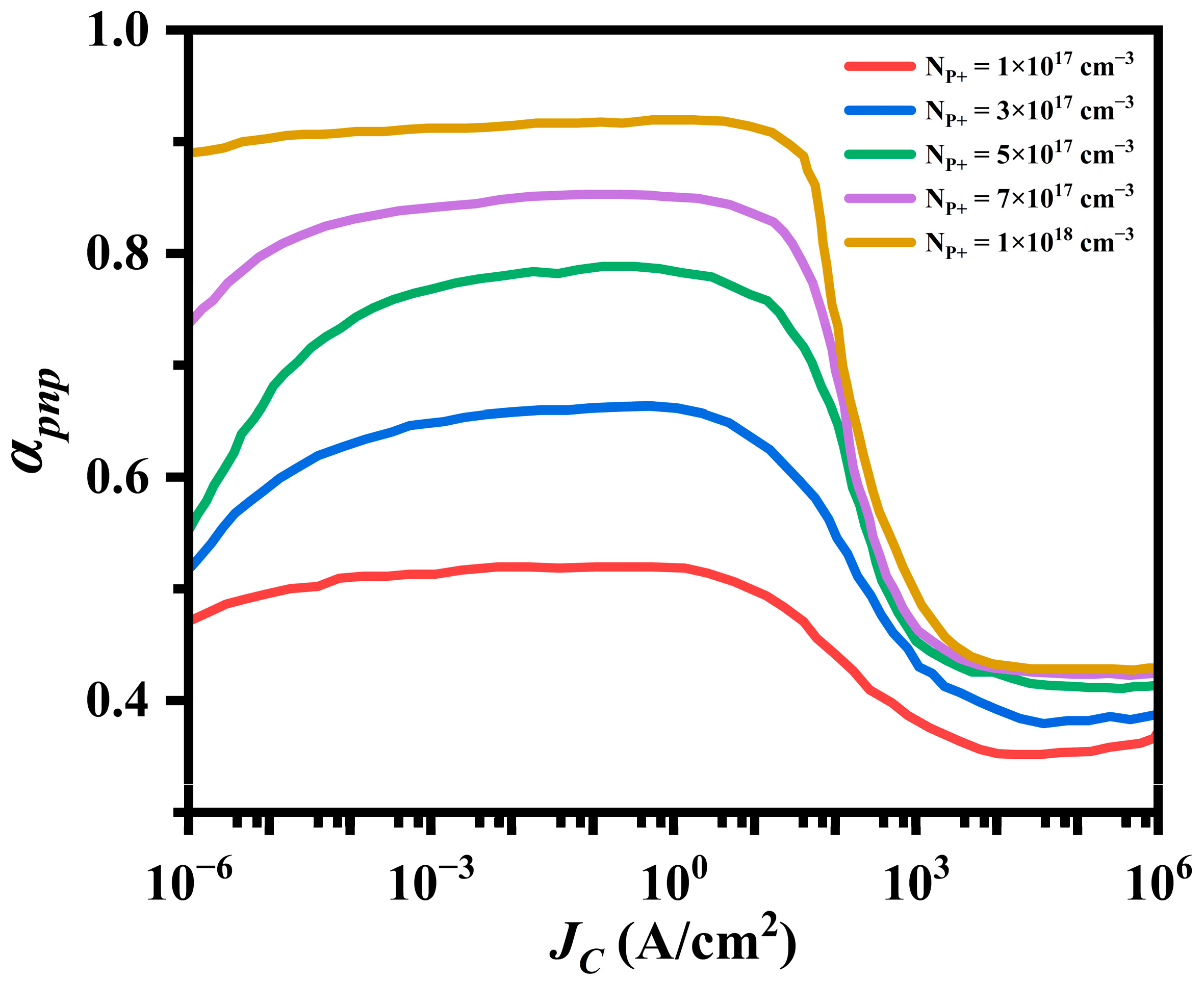
2.2. The Impact of αpnp

From the analysis presented above, the FS-IGBT avalanche breakdown curve is primarily characterized by the existence of the NDR1 branch. The primary cause of this branch’s formation is backside hole injection, while the αpnp of the device controls the extent of the hole injection. Consequently, αpnp is a critical factor influencing the avalanche breakdown characteristics of FS-IGBT.
A comparison of simulated avalanche breakdown characteristic curves for five FS-IGBTs with different collector doping concentrations of NP+ is shown in Figure 4. As the NP+ concentration in the FS-IGBT increases, the αpnp at the same JC becomes larger, resulting in a lower VCE at this JC value. Furthermore, with increasing NP+, the valley point V corresponds to a higher JC value. Figure 5 shows the variation in αpnp with collector current density JC for five FS-IGBTs operating in avalanche breakdown mode, as extracted by simulation. As JC increases from the level of leakage current, the FS layer transitions from low to high injection, resulting in a gradual increase in Lp,eff and αpnp, as noted in Equation (3). When JC is increased sufficiently to inject a substantial number of carriers into the FS layer, the hole injection efficiency γp at junction J1 decreases significantly, leading to a sharp decrease in αpnp. This explains why the avalanche breakdown curve of the FS-IGBT transitions from the NDR1 branch to the PDR branch. From Figure 5, it is also evident that as NP+ increases, the JC corresponding to the sharp decrease in αpnp also increases. This occurs because for γp to decrease as NP+ increases, the density of holes injected into the FS layer must increase; consequently, JC must also increase. In summary, the larger the αpnp of the FS-IGBT, the stronger the negative differential resistance (NDR1) effect, and the higher the JC value corresponding to the valley point V of VCE.

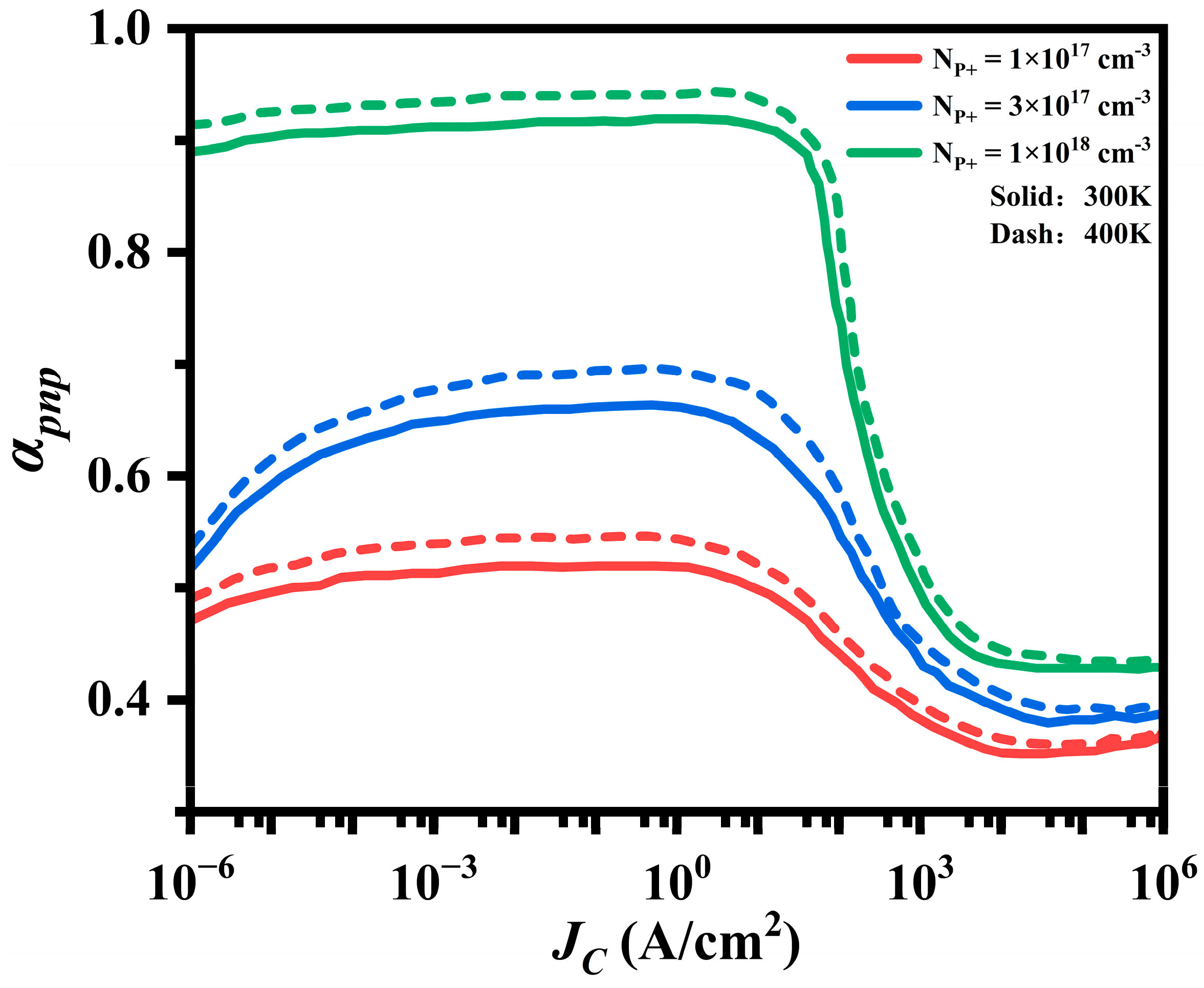
2.3. The Impact of Temperature

Figure 6 displays the avalanche breakdown characteristic curves of 650 V FS-IGBTs with varying NP+ at room and high temperatures, while Figure 7 illustrates the corresponding relationship curves between αpnp and the collector current density JC. As observed in Figure 7, αpnp increases with temperature, attributable to the extended carrier lifetimes. Although an increase in αpnp leads to a decrease in avalanche breakdown voltage, it is also important to note that a rise in temperature reduces the collision current rate of electrons and holes [23,24], thereby increasing the avalanche breakdown voltage, as demonstrated in Figure 6. Additionally, it is observed that the higher the NP+ in FS-IGBTs, the smaller the valley offset ΔVCE across their high and low-temperature avalanche breakdown curves.

3. Properties of the Current Filament

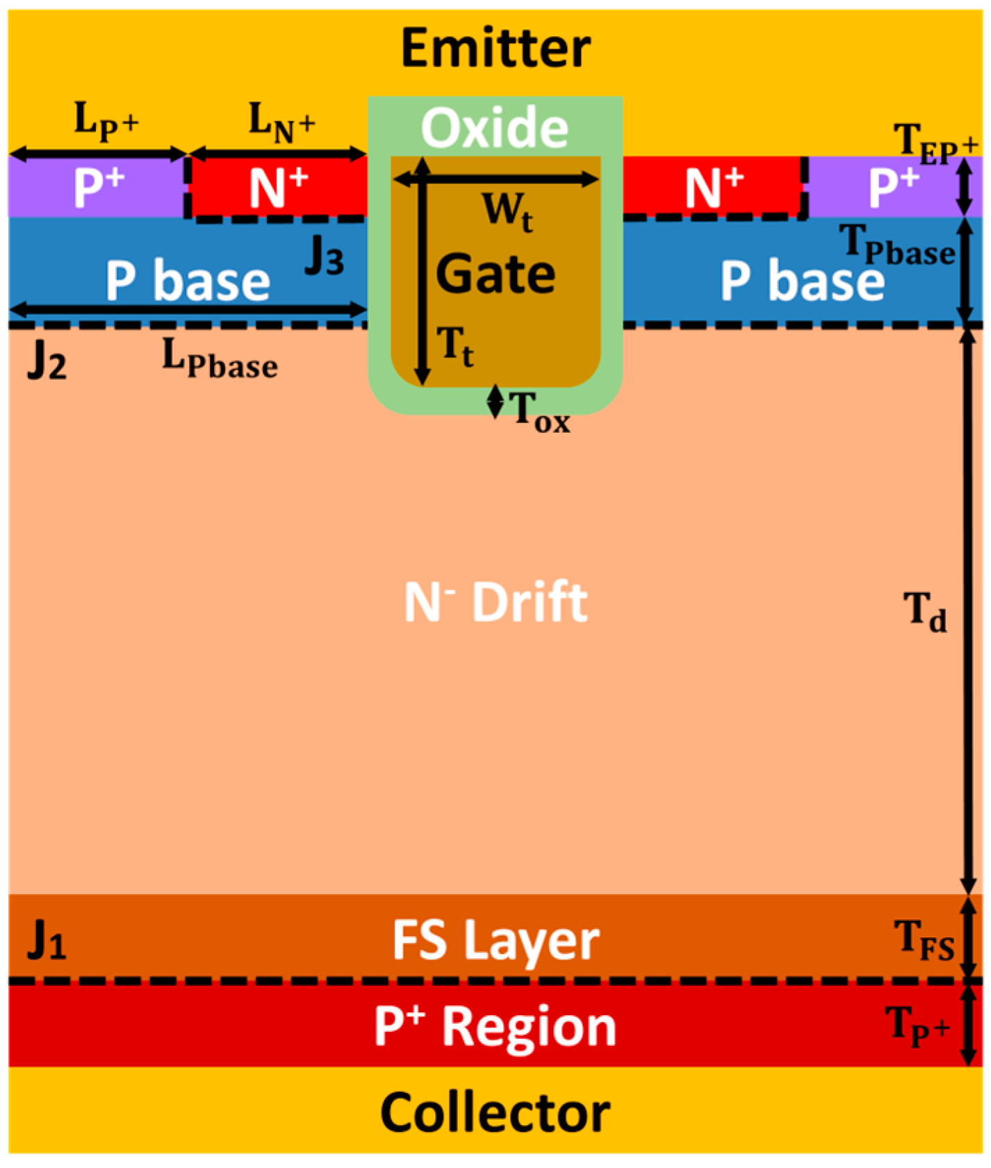
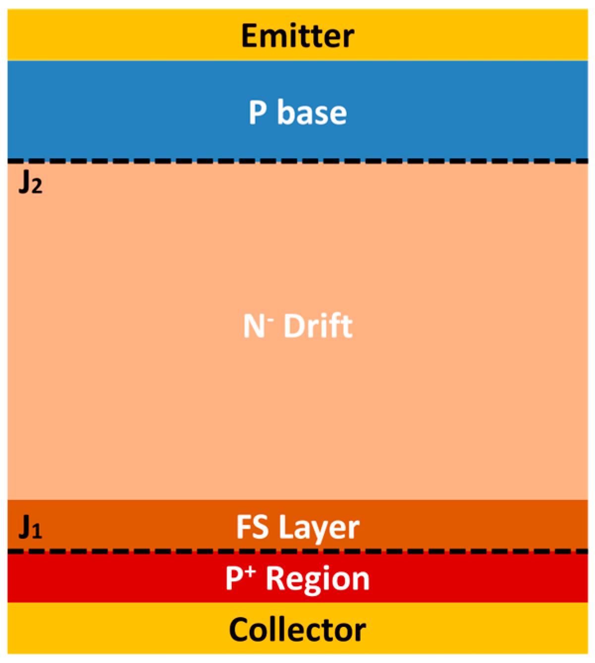
3.1. Structural Model and Simulation Method

Since the front MOS channel of the FS-IGBT is closed in the blocking state, the MOS structure remains inactive. To enhance simulation efficiency, the backside PNP transistor structure is extracted from the 650 V FS-IGBT and employed to simulate the avalanche-generating current filament, as depicted in Figure 8. The total simulated width of the device is 400 µm, corresponding to the width of the 200 cells shown in Figure 1.

3.2. Physical Mechanisms for Controlling the Strength of Current Filament

The NDR branch on the device’s avalanche breakdown curve drives the enhancement of current filaments [25,26]. This occurs because, on the NDR branch, the voltage across the device decreases as the avalanche current increases, as illustrated on the NDR branch in Figure 2. If the device has generated a current filament, causing the current to converge in a specific region while operating on the NDR branch. The voltage in this region decreases due to the increasing current density. Consequently, the differential resistance in this region tends to decrease relative to other regions, leading to further concentration of current and creating positive feedback. This results in increasing current density at the center of the current filament. If the device operates on the PDR branch, the concentration of current in a specific region leads to increased differential resistance compared to other regions, thus discouraging the concentration of current in that region. In summary, if the NDR branch is stronger, the voltage VCE at both ends of the device decreases more rapidly with increasing current density. The stronger negative differential resistance effect leads to faster aggregation of currents toward the region where the current filaments are located. The current filament intensifies until the operating state of this region transitions to the PDR branch.
Therefore, theoretically predicting the maximum strength of the current filament generated by a device requires determining the magnitude of the avalanche current at which its avalanche breakdown curve transitions from the NDR branch to the PDR branch, as represented by the current at the valley point V in Figure 2. The higher the current density at the valley point V, the stronger the current filament generated by the device becomes. As a result, the larger the αpnp of the FS-IGBT, the stronger the current filament in avalanche mode, thereby reducing the device’s robustness.

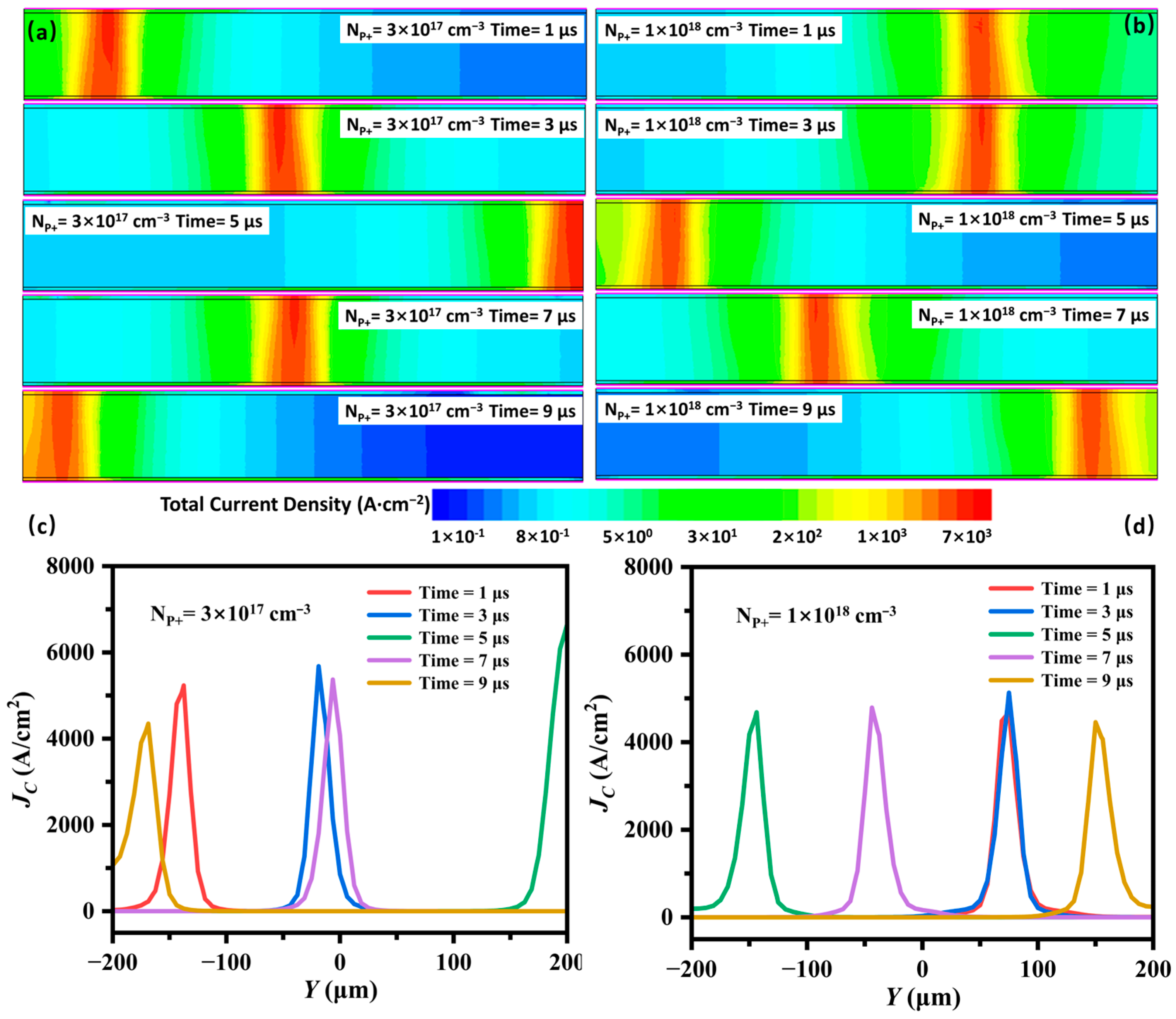
3.3. Physical Mechanisms for Driving the Movement of Current Filament

The reliability of IGBTs is affected not only by the strength of the current filament but also by its mobility [27,28]. Figure 9 shows the simulated time-dependent VCE curves for two FS-IGBTs operating in avalanche mode with NP+ = 3 × 1017 cm−3 and NP+ = 1 × 1018 cm−3 at constant temperature. ICE is the pulse current applied identically to both devices. The current density distribution inside the device is shown in Figure 10. Since the pulse current ICE = 200 A, both devices operate on the NDR1 branch of the avalanche breakdown curve shown in Figure 2, resulting in the VCE in Figure 9 reaching a peak value as ICE increases, then dropping rapidly due to the NDR effect. Due to the higher NP+ and the stronger NDR effect, the VCE at NP+ = 1 × 1018 cm−3 decreases more significantly than that at NP+ = 3 × 1017 cm−3. Observations of the current density distribution inside the device and the current filament generated by the avalanche reveal that the current filament has remained fixed at its original position since its formation and has not moved over time. This stability explains why the VCE curve shown in Figure 9 remains unchanged.
The above thermostatic simulation results indicate that the current filament generated by the FS-IGBT in avalanche mode remains stationary because the simulation does not account for the effects of temperature rise. Therefore, thermoelectric simulations were conducted under identical pulse current conditions for both 650 V FS-IGBT devices with NP+ = 3 × 1017 cm−3 and NP+ = 1 × 1018 cm−3. The simulated curves of VCE and the maximum lattice temperature Tmax over time are shown in Figure 11. Variations in the current density distribution during device operation in avalanche mode are depicted in Figure 12a–d. As seen in Figure 11 and Figure 12, a fast-moving current filament is generated inside the device. This occurs because the NDR1 branch on the avalanche breakdown curve of the FS-IGBT shifts toward a higher VCE as the temperature increases. The generation of a current filament increases the temperature and differential resistance within a region of the device, prompting the current filament to move toward regions with lower temperature and differential resistance. The phenomenon of current filament movement has been experimentally observed in the literature [8,24,29,30,31], consistent with our simulation and theoretical analysis.
In Figure 12a, when NP+ = 3 × 1017 cm−3, the current filament moves from the leftmost to the rightmost end at 5 μs. At 9 μs, the current filament has returned to the leftmost end. In Figure 12b, when NP+ = 1 × 1018 cm−3, the current filament only moves about half of the device width at 5 μs and does not complete an entire round trip even at 9 μs. From this, it can be analyzed that although the current filament with NP+ = 1 × 1018 cm−3 moves significantly slower than that with NP+ = 3 × 1017 cm−3. This difference is attributed to the variation in the offset ΔVCE of the NDR1 branch caused by the temperature rise, as shown in Figure 6. A larger offset ΔVCE results in a higher positive differential resistance due to the temperature increase at the current filament’s location, facilitating its movement towards areas of lower temperature. The slower movement of the current filament, leading to its prolonged presence in one area, results in a more significant temperature increase, as evidenced by the lattice temperature variations shown in Figure 11 and Figure 12. This increase in temperature reduces the robustness of the device.
It should be noted that the lattice temperature is higher for NP+ = 1 × 1018 cm−3 during the same temperature jump cycle as shown in Figure 11. However, at NP+ = 3 × 1017 cm−3, the current filament moves to the device boundary and then shifts in the opposite direction. Consequently, the temperature changes more frequently, resulting in higher maximum lattice temperatures Tmax for the device at NP+ = 3 × 1017 cm−3 than for NP+ = 1 × 1018 cm−3 during specific intervals. This discrepancy can be attributed to the limitations of device simulation [32,33], given that real devices consist of thousands of cells. The movement of a current filament from one boundary of the device to another takes considerable time, and multiple current filaments may be generated. Therefore, the maximum lattice temperature Tmax of NP+ = 1 × 1018 cm−3 is expected to be higher than that of NP+ = 3 × 1017 cm−3 in real devices.

4. Conclusions

During an avalanche breakdown in an IGBT, the avalanche electrons generated at junction J2 move toward the collector side. This movement leads to a hole injection in the backside collector region, which results in the formation of an additional negative differential resistance (NDR) branch on the avalanche breakdown curve. This unique NDR1 branch is the primary feature distinguishing IGBTs from diodes.
The avalanche current JC at the valley point V on the IGBT avalanche breakdown curve, during the transition from the NDR1 to the PDR branch, is the primary factor influencing the strength of the current filament. The offset ΔVCE of the avalanche breakdown curve at high and low temperatures plays a crucial role in regulating the movement speed of the current filament. Both of these factors are predominantly determined by αpnp. When αpnp of the IGBT is higher, the negative differential resistance effect of the NDR1 branch is stronger, and the avalanche current JC at the valley point V, as the curve transitions from the NDR1 to the PDR branch, is higher, leading to a stronger avalanche current filament. Moreover, as αpnp increases, the offset ΔVCE of the avalanche breakdown curve at high and low temperatures decreases, resulting in a slower movement of the current filament and a higher temperature rise of the device. As a result, the avalanche robustness of the IGBT decreases with increasing αpnp. Therefore, it is crucial to find a balance in controlling αpnp during device design.

Author Contributions

Conceptualization, J.Z., H.L. and H.W.; methodology, J.Z., H.L. and H.W.; software, J.Z. and H.L.; validation, J.Z., H.L. and H.W.; formal analysis, J.Z.; investigation, J.Z., H.L. and B.Z.; resources, H.W., B.Z., X.C., G.Z., P.F. and S.W.; data curation, J.Z.; writing—original draft preparation, J.Z.; writing—review and editing, S.W.; visualization, J.Z., B.Z., X.C., G.Z. and P.F.; supervision, S.W.; project administration, S.W.; funding acquisition, X.C., G.Z., P.F. and S.W. All authors have read and agreed to the published version of the manuscript.

Funding

This research was funded by the National Natural Science Foundation of China under Grant No. 62071073, the Fundamental Research Funds for Central Universities under Grant No. 2023CDJXY-041, and the Foundation from Guangxi Key Laboratory of Optoelectronic Information Processing under Grant No. GD20201.

Data Availability Statement

The original contributions presented in the study are included in the article, further inquiries can be directed to the corresponding author.

Conflicts of Interest

The authors declare no conflicts of interest.

References

  1. Baburske, R.; Lutz, J.; Heinze, B. Effects of Negative Differential Resistance in High Power Devices and Some Relations to DMOS Structures. In Proceedings of the 2010 IEEE International Reliability Physics Symposium, Garden Grove, CA, USA, 2–6 May 2010; IEEE: Garden Grove, CA, USA, 2010; pp. 162–169. [Google Scholar]
  2. Lutz, J.; Baburske, R. Dynamic Avalanche in Bipolar Power Devices. Microelectron. Reliab. 2012, 52, 475–481. [Google Scholar] [CrossRef]
  3. Hower, P.L.; Krishna Reddi, V.G. Avalanche Injection and Second Breakdown in Transistors. IEEE Trans. Electron Devices 1970, 17, 320–335. [Google Scholar] [CrossRef]
  4. Baburske, R.; Niedernostheide, F.-J.; Lutz, J.; Schulze, H.-J.; Falck, E.; Bauer, J.G. Cathode-Side Current Filaments in High-Voltage Power Diodes Beyond the SOA Limit. IEEE Trans. Electron Devices 2013, 60, 2308–2317. [Google Scholar] [CrossRef]
  5. Oetjen, J.; Jungblut, R.; Kuhlmann, U.; Arkenau, J.; Sittig, R. Current lamentation in Bipolar Power Devices during Dynamic Avalanche Breakdown. Solid-State Electron. 2000, 44, 117–123. [Google Scholar] [CrossRef]
  6. Toechterle, C.; Pfirsch, F.; Sandow, C.; Wachutka, G. Analysis of the Latch-up Process and Current Filamentation in High-Voltage Trench-IGBT Cell Arrays. In Proceedings of the 2013 International Conference on Simulation of Semiconductor Processes and Devices (SISPAD), Glasgow, UK, 3–5 September 2013; IEEE: Glasgow, UK, 2013; pp. 296–299. [Google Scholar]
  7. Suwa, T. 2D-TCAD Simulation Study of Capture Layer and Repellent Layer of Current Filament in Trench-Gate IGBTs. In Proceedings of the 2021 International Conference on Simulation of Semiconductor Processes and Devices (SISPAD), Dallas, TX, USA, 27–29 September 2021; IEEE: Dallas, TX, USA, 2021; pp. 32–35. [Google Scholar]
  8. Endo, K.; Nagamine, S.; Saito, W.; Matsudai, T.; Ogura, T.; Setoya, T.; Nakamae, K. Direct Photo Emission Motion Observation of Current Filaments in the IGBT under Avalanche Breakdown Condition. In Proceedings of the 2016 28th International Symposium on Power Semiconductor Devices and ICs (ISPSD), Prague, Czech Republic, 12–16 June 2016; IEEE: Prague, Czech Republic, 2016; pp. 367–370. [Google Scholar]
  9. Bhojani, R.; Kowalsky, J.; Lutz, J.; Kendig, D.; Baburske, R.; Schulze, H.-J.; Niedernostheide, F.-J. Observation of Current Filaments in IGBTs with Thermoreflectance Microscopy. In Proceedings of the 2018 IEEE 30th International Symposium on Power Semiconductor Devices and ICs (ISPSD), Chicago, IL, USA, 13–17 May 2018; IEEE: Chicago, IL, USA, 2018; pp. 164–167. [Google Scholar]
  10. Toechterle, C.; Pfirsch, F.; Sandow, C.; Wachutka, G. Evolution of Current Filaments Limiting the Safe-Operating Area of High-Voltage Trench-IGBTs. In Proceedings of the 2014 IEEE 26th International Symposium on Power Semiconductor Devices & IC’s (ISPSD), Waikoloa, HI, USA, 15–19 June 2014; IEEE: Waikoloa, HI, USA, 2014; pp. 135–138. [Google Scholar]
  11. Muller-Dauch, A.; Pfirsch, F.; Pfaffenlehner, M.; Silber, D. Source Side Thermal Runaway of Trench IGBTs, Dependence on Design Aspects. In Proceedings of the 2006 IEEE International Symposium on Power Semiconductor Devices & IC’s, Naples, Italy, 4–8 June 2006; IEEE: Naples, Italy, 2006; pp. 1–4. [Google Scholar]
  12. Tanaka, M.; Abe, N.; Nakagawa, A. Impact of 3D Simulation on the Analysis of Unclamped Inductive Switching. Jpn. J. Appl. Phys. 2020, 59, SGGD01. [Google Scholar] [CrossRef]
  13. Egawa, H. Avalanche Characteristics and Failure Mechanism of High Voltage Diodes. IEEE Trans. Electron Devices 1966, ED-13, 754–758. [Google Scholar] [CrossRef]
  14. Lutz, J.; Baburske, R.; Chen, M.; Heinze, B.; Domeij, M.; Felsl, H.-P.; Schulze, H.-J. The nn+Junction as the Key to Improved Ruggedness and Soft Recovery of Power Diodes. IEEE Trans. Electron Devices 2009, 56, 2825–2832. [Google Scholar] [CrossRef]
  15. Domeij, M.; Lutz, J.; Silber, D. On the Destruction Limit of Si Power Diodes during Reverse Recovery with Dynamic Avalanche. IEEE Trans. Electron Devices 2003, 50, 486–493. [Google Scholar] [CrossRef]
  16. Heinze, H.P.F. Influence of Buffer Structures on Static and Dynamic Ruggedness of High Voltage FWDs. In Proceedings of the ISPSD ’05. The 17th International Symposium on Power Semiconductor Devices and ICs, Santa Barbara, CA, USA, 23–26 May 2005; IEEE: Santa Barbara, CA, USA, 2005; pp. 215–218. [Google Scholar]
  17. Knipper, U.; Wachutka, G.; Pfirsch, F.; Raker, T.; Niedermeyr, J. Time-Periodic Avalanche Breakdown at the Edge Termination of Power Devices. In Proceedings of the 2008 20th International Symposium on Power Semiconductor Devices and IC’s, Orlando, FL, USA, 18–22 May 2008; IEEE: Orlando, FL, USA, 2008; pp. 307–310. [Google Scholar]
  18. Lophitis, N.; Antoniou, M.; Udrea, F.; Wikstrom, T.; Nistor, I. Turn-off Failure Mechanism in Large Area IGCTs. In Proceedings of the CAS 2011 Proceedings (2011 International Semiconductor Conference), Sinaia, Romania, 17–19 October 2011; IEEE: Sinaia, Romania, 2011; pp. 361–364. [Google Scholar]
  19. Spirito, P.; Breglio, G.; Irace, A.; Maresca, L.; Napoli, E.; Riccio, M. Physics of the Negative Resistance in the Avalanche IV Curve of Field Stop IGBTs: Collector Design Rules for Improved Ruggedness. IEEE Trans. Electron Devices 2014, 61, 1457–1463. [Google Scholar] [CrossRef]
  20. Baliga, B.J. Analytical Modeling of IGBTs: Challenges and Solutions. IEEE Trans. Electron Devices 2013, 60, 535–543. [Google Scholar] [CrossRef]
  21. Andreas Muller, F.P. Trench IGBT Behaviour near to Latch-up Conditions. In Proceedings of the Proceedings. ISPSD ’05. The 17th International Symposium on Power Semiconductor Devices and ICs, Santa Barbara, CA, USA, 23–26 May 2005; IEEE: Santa Barbara, CA, USA, 2005; pp. 255–258. [Google Scholar]
  22. Wang, C.; Zhang, L. Peak Electric Field Shifting Induced by Avalanche Injection under Static Avalanche in High Voltage Diode. IEICE Electron. Express 2017, 14, 20170627. [Google Scholar] [CrossRef]
  23. Baliga, B.J. Fundamentals of Power Semiconductor Devices; Springer: New York, NY, USA, 2008; ISBN 978-0-387-47313-0. [Google Scholar]
  24. Breglio, G.; Irace, A.; Napoli, E.; Riccio, M.; Spirito, P. Experimental Detection and Numerical Validation of Different Failure Mechanisms in IGBTs During Unclamped Inductive Switching. IEEE Trans. Electron Devices 2013, 60, 563–570. [Google Scholar] [CrossRef]
  25. Knipper, U.; Pfirsch, F.; Raker, T.; Niedermeyr, J.; Wachutka, G. Destruction in the Active Part of an IGBT Chip Caused by Avalanche-Breakdown at the Edge Termination Structure. In Proceedings of the 2008 International Conference on Advanced Semiconductor Devices and Microsystems, Smolenice, Slovakia, 12–16 October 2008; IEEE: Smolenice, Slovakia, 2008; pp. 159–162. [Google Scholar]
  26. Felsl, H.P.; Falck, E.; Niedernostheide, F.-J.; Milady, S.; Silber, D.; Lutz, J. Electro-Thermal Simulation of Current Filamentation in 3.3-kV p+-n-n+ Diodes with Differenth Edge Terminations. In Proceedings of the 2006 IEEE International Symposium on Power Semiconductor Devices & IC’s, Naples, Italy, 4–8 June 2006; IEEE: Naples, Italy, 2006; pp. 1–4. [Google Scholar]
  27. Niedernostheide, F.-J.; Falck, E.; Schulze, H.-J.; Kellner-Werdehausen, U. Influence of Joule Heating on Current Filaments Induced by Avalanche Injection. IEE Proc. Circuits Devices Syst. 2006, 153, 3. [Google Scholar] [CrossRef]
  28. Tong, X.; Liu, S.; Sun, W.; Wu, J. Complete Avalanche Process and Failure Mechanism of Trench-Gate FS-IGBT Under Unclamped Inductive Switching by Using Infrared Visualization Method. IEEE Trans. Electron Devices 2020, 67, 3908–3911. [Google Scholar] [CrossRef]
  29. Riccio, M.; Irace, A.; Breglio, G.; Spirito, P.; Napoli, E.; Mizuno, Y. Electro-Thermal Instability in Multi-Cellular Trench-IGBTs in Avalanche Condition: Experiments and Simulations. In Proceedings of the 2011 IEEE 23rd International Symposium on Power Semiconductor Devices and ICs, San Diego, CA, USA, 23–26 May 2011; IEEE: San Diego, CA, USA, 2011; pp. 124–127. [Google Scholar]
  30. Endo, K.; Nakamae, K. Temporally- and Spatially-Resolved Observations of Current Filament Dynamics in Insulated Gate Bipolar Transistor Chip During Avalanche Breakdown. IEEE Trans. Device Mater. Relib. 2019, 19, 723–727. [Google Scholar] [CrossRef]
  31. Shankar, B.; Zeng, K.; Gunning, B.; Martinez, R.P.; Meng, C.; Flicker, J.; Binder, A.; Dickerson, J.R.; Kaplar, R.; Chowdhury, S. Movement of Current Filaments and Its Impact on Avalanche Robustness in Vertical GaN P-N Diode Under UIS Stress. In Proceedings of the 2022 Device Research Conference (DRC), Columbus, OH, USA, 26 June 2022; IEEE: Columbus, OH, USA, 2022; pp. 1–2. [Google Scholar]
  32. Shiba, Y.; Omura, I.; Tsukuda, M. IGBT Avalanche Current Filamentaion Ratio: Precise Simulations on Mesh and Structure Effect. In Proceedings of the 2016 28th International Symposium on Power Semiconductor Devices and ICs (ISPSD), Prague, Czech Republic, 12–16 June 2016; IEEE: Prague, Czech Republic, 2016; pp. 339–342. [Google Scholar]
  33. Watanabe, M.; Shigyo, N.; Hoshii, T.; Furukawa, K.; Kakushima, K.; Satoh, K.; Matsudai, T.; Saraya, T.; Takakura, T.; Itou, K.; et al. Impact of Three-Dimensional Current Flow on Accurate TCAD Simulation for Trench-Gate IGBTs. In Proceedings of the 2019 31st International Symposium on Power Semiconductor Devices and ICs (ISPSD), Shanghai, China, 19–23 May 2019; IEEE: Shanghai, China, 2019; pp. 311–314. [Google Scholar]
Figure 1. Cross-sectional view of the 650 V trench FS-IGBT.
Electronics 13 02347 g001
Figure 2. The simulated avalanche breakdown curve of the 650 V FS-IGBT (T = 300 K, NP+ = 3 × 1017 cm−3).
Electronics 13 02347 g002
Figure 3. Vertical distributions of the electric field along the FS-IGBT at different avalanche currents.
Electronics 13 02347 g003
Figure 4. The simulated avalanche breakdown curves of the 650 V FS-IGBT with a different NP+ (T = 300 K).
Electronics 13 02347 g004
Figure 5. The αpnp for the 650 V FS-IGBT with different NP+s as a function of JC.
Electronics 13 02347 g005
Figure 6. The avalanche breakdown curves of the 650 V FS-IGBT with different NP+s at high and low temperatures.
Electronics 13 02347 g006
Figure 7. The αpnp for the 650 V FS-IGBT with different NP+s as a function of JC at high and low temperatures.
Electronics 13 02347 g007
Figure 8. The structure model of the 650 V FS-IGBT is used to simulate the current filament at the static avalanche.
Electronics 13 02347 g008
Figure 9. Simulated time-dependent VCE curves for the two FS-IGBTs with different NP+ operating in avalanche mode at constant temperature (the applied pulse current is 200 A, the rise time is 1 µs).
Electronics 13 02347 g009
Figure 10. (a) Simulated current density distributions inside the FS-IGBTs with different NP+ operating in avalanche mode at constant temperature and (b) lateral current density distribution along the J2 junction.
Electronics 13 02347 g010
Figure 11. Simulated time-dependent VCE and maximum lattice temperature Tmax for the two FS-IGBTs with different NP+ operating in avalanche mode in the thermoelectric case (the applied pulse current is 200 A, the rise time is 1 µs).
Electronics 13 02347 g011
Figure 12. Simulated current density distributions inside the FS-IGBTs with a different NP+ operating in avalanche mode in the thermoelectric case. 2-D current density distributions with (a) NP+ = 3 × 1017 cm−3 and (b) NP+ = 1 × 1018 cm−3, lateral current density with (c) NP+ = 3 × 1017 cm−3 and (d) NP+ = 1 × 1018 cm−3.
Electronics 13 02347 g012
Table 1. Simulation parameters of the 650 V trench FS-IGBT.
SymbolStructure ParameterValue
TP+Collector P+ region depth1.0 μm
NP+Collector P+ region doping concentration3.0 × 1017 cm−3
TFSFS layer depth2.0 μm
NFSFS layer doping concentration3.0 × 1016 cm−3
TdDrift thickness62.0 μm
NdDrift doping concentration1.0 × 1014 cm−3
TtGate trench depth5.0 μm
WtGate trench width1.0 μm
ToxGate oxide thickness0.12 μm
TPbaseP base depth3.0 μm
LPbaseP base length1.0 μm
NPbaseP base doping concentration1.0 × 1017 cm−3
TN+N+ depth0.3 μm
LN+N+ length0.5 μm
NN+N+ doping concentration1.0 × 1020 cm−3
TEP+P+ depth0.3 μm
LEP+P+ length0.5 μm
NEP+P+ doping concentration1.0 × 1020 cm−3
Disclaimer/Publisher’s Note: The statements, opinions and data contained in all publications are solely those of the individual author(s) and contributor(s) and not of MDPI and/or the editor(s). MDPI and/or the editor(s) disclaim responsibility for any injury to people or property resulting from any ideas, methods, instructions or products referred to in the content.

