Article

Modeling and Suppression of Conducted Interference in Flyback Power Supplies Based on GaN Devices

1
Key Laboratory of Advanced Manufacturing and Automation Technology, Guilin University of Technology, Education Department of Guangxi Zhuang Autonomous Region, Guilin 541006, China
2
College of Mechanical and Control Engineering, Guilin University of Technology, Guilin 541006, China
3
Greatwall Power Supply Technology Co., Ltd., Shenzhen 518000, China
*
Author to whom correspondence should be addressed.
Electronics 2024, 13(12), 2360; https://doi.org/10.3390/electronics13122360
Submission received: 15 May 2024 / Revised: 4 June 2024 / Accepted: 6 June 2024 / Published: 16 June 2024
(This article belongs to the Topic Advances in Power Science and Technology)

Abstract

:
The application of GaN power devices has significantly increased the power density of flyback power supplies but has also caused severe electromagnetic interference (EMI) issues. To address the challenge of conducted interference in flyback power supplies, a comprehensive analysis of the transmission mechanism of conducted common-mode noise is undertaken. This analysis involves simplifying the equivalent model of conducted interference and leveraging the circuit characteristics of conducted noise to propose a solution for attenuating common-mode noise. Considering the constraints of external compensation capacitors, a balanced winding is further introduced to mitigate the impact of noise. To enhance the efficacy of conducted interference suppression, it is suggested to change the winding structure of the transformer and incorporate a shielding winding. This configuration aims to minimize the generation and propagation of common-mode noise within the transformer. Finally, experimental verification is carried out using a 150 W GaN flyback power supply prototype. The experimental results demonstrate that the proposed method effectively suppresses common-mode noise in the circuit.

1. Introduction

Flyback converters are renowned for their simple structure, requiring fewer components while providing a stable output and high efficiency. They are commonly used in low- and medium-power supplies. As the demand for higher efficiency and power density in power supplies increases, wide-bandgap semiconductor devices such as Gallium Nitride (GaN) and Silicon Carbide (SiC) are being increasingly employed. These devices exhibit superior switching characteristics, enabling power supplies to operate at ultrahigh switching frequencies. Consequently, this significantly enhances power density and reduces power losses in power supplies [1,2,3,4]. Power converters based on GaN devices achieve higher switching frequencies but are also associated with higher dv/dt and di/dt conversion rates, generating electromagnetic interference (EMI) noise that can disrupt low-voltage electronics and sensitive digital circuits [5,6]. To meet electromagnetic compatibility requirements, EMI filters are widely used in flyback converters. However, the typical volume of EMI filters constitutes about one-third of the converter, which is not conducive to cost savings and power density improvement [7,8]. This study aims to investigate the noise sources and propagation paths of flyback power supplies based on GaN devices, establish a noise propagation model, and propose an effective common-mode noise suppression method. The goal is to reduce the inherent noise of the flyback power supply, simplify the design of EMI filters, and thereby decrease the size and weight of these filters, ultimately improving the power density of the power supply.
Current research on the suppression of converter conduction interference primarily focuses on the following aspects: direct suppression at the noise source, effective cutoff or compensation of the noise propagation path, and offsetting of the displacement current. Reference [9] analyzed the conduction paths of the flyback common-mode interference current, measured the equivalent common-mode capacitance values on different paths, and suppressed the interference by balancing the primary and secondary common-mode currents to reduce the total common-mode displacement current to zero. Reference [10] proposed, for multi-output flyback converters, that the boost converter should take two isolated and one non-isolated output to prevent voltage spikes in the coupling inductors and reduce device stress, thereby reducing electromagnetic interference. Reference [11] suggested placing a switching tube between the two coils to equalize noise using the symmetry of the primary coils; however, this method complicates the circuit and is difficult to control, making its feasibility low. References [12,13,14] proposed altering the distributed capacitance between windings by changing the transformer structure and winding method, thereby improving the system’s EMC characteristics. Using copper foil shielding for transformers to suppress common-mode noise is also common, but the overall design theory guidance is insufficient [15]. Reference [16] utilized core shielding to address the coupling problem caused by the transformer core and employed a converter to solve the issues of multi-Y capacitance and capacitive filtering, providing better EMI suppression compared to conventional pulse-width modulation. Reference [17] highlighted the significant influence of transformer common-mode coupling capacitance on noise suppression and demonstrated that the feasibility of the transformer can be verified without an EMI receiver, using only a signal generator and an oscilloscope. References [18,19,20] incorporated balanced winding techniques to achieve effective shielding and offset common-mode noise, and they provided a theoretical method for calculating the number of turns in a balanced winding, which is valuable for this study. The common-mode noise coupling mechanism proposed in references [11,21,22,23] is more challenging to understand, and although it performs detailed modeling reasoning, the introduced shielding layer in the transformer is overly complex. References [16,24,25,26] discuss the integration of shielded windings and the modeling of capacitance distribution in flyback converters, which serves as a good guide for transformer EMC design. Reference [27] analyzes the EMI characteristics of wide-bandwidth semiconductor power systems, facilitating a subsequent analysis of conducted interference propagation.
Based on recent studies on conducted interference suppression, several methods are available to directly cancel common-mode noise or suppress it within the noise loop; however, their general applicability is limited. This paper proposes three methods to suppress common-mode noise interference in GaN flyback power supplies and provides a detailed analysis of each method. An experimental platform is constructed using a 150 W GaN flyback power supply, and the experimental results validate the effectiveness and feasibility of the proposed methods.
The rest of the paper is organized as follows. Section 2 describes the common-mode noise transmission mechanism in GaN-based flyback power supplies. Section 3 details three methods for common-mode noise suppression. The experimental results and conclusions are presented in Section 4 and Section 5, respectively.

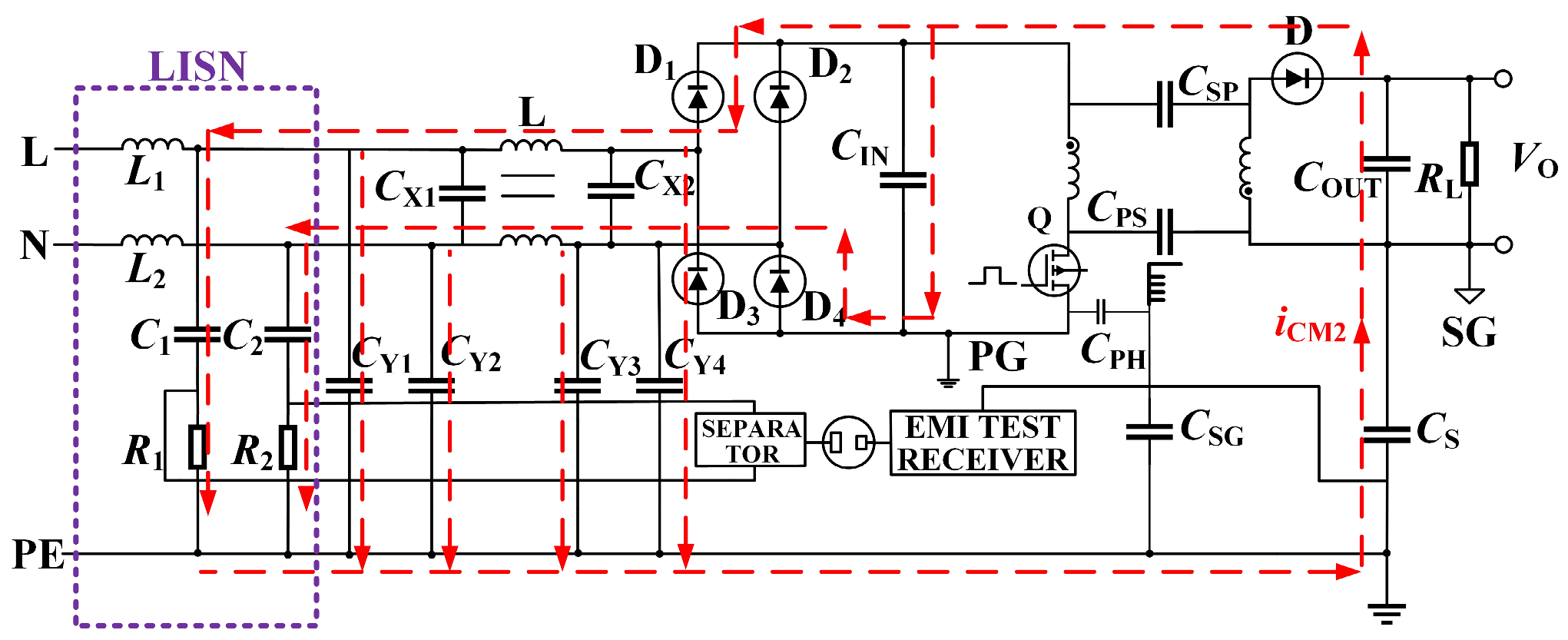
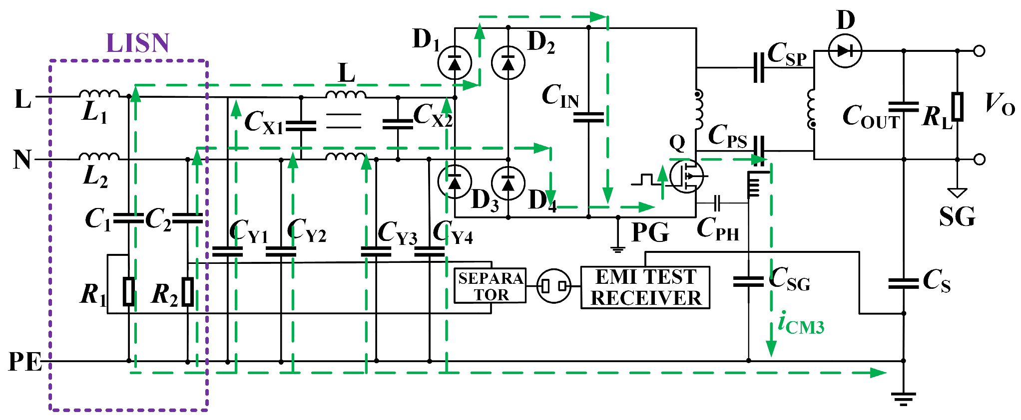
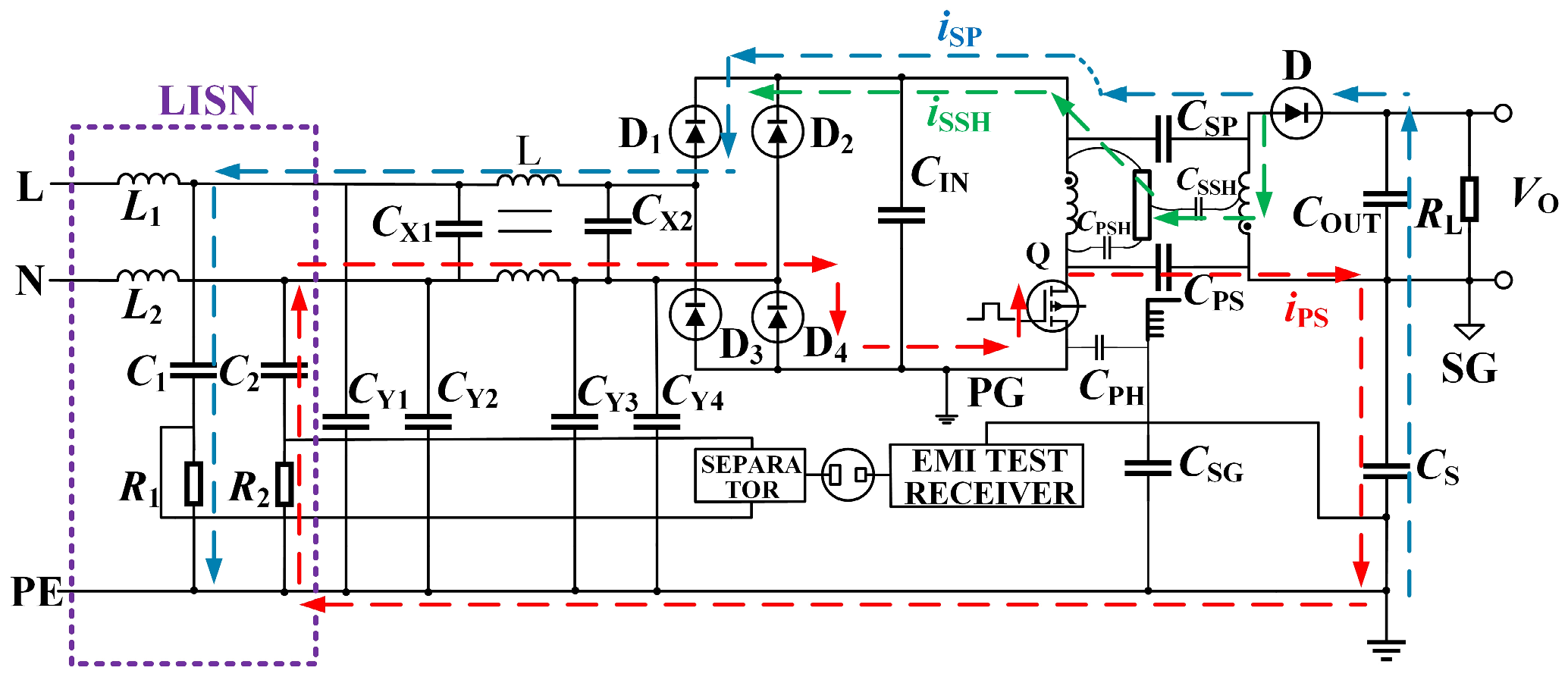
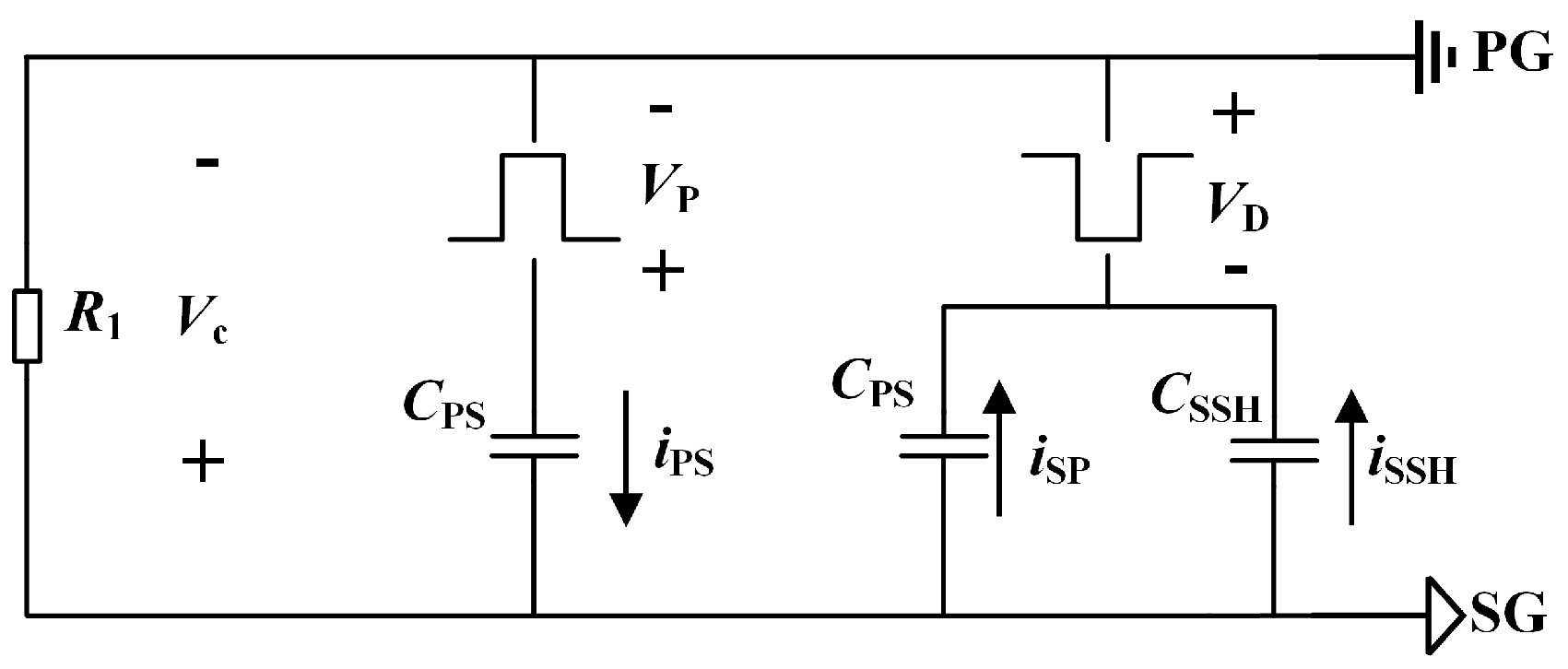
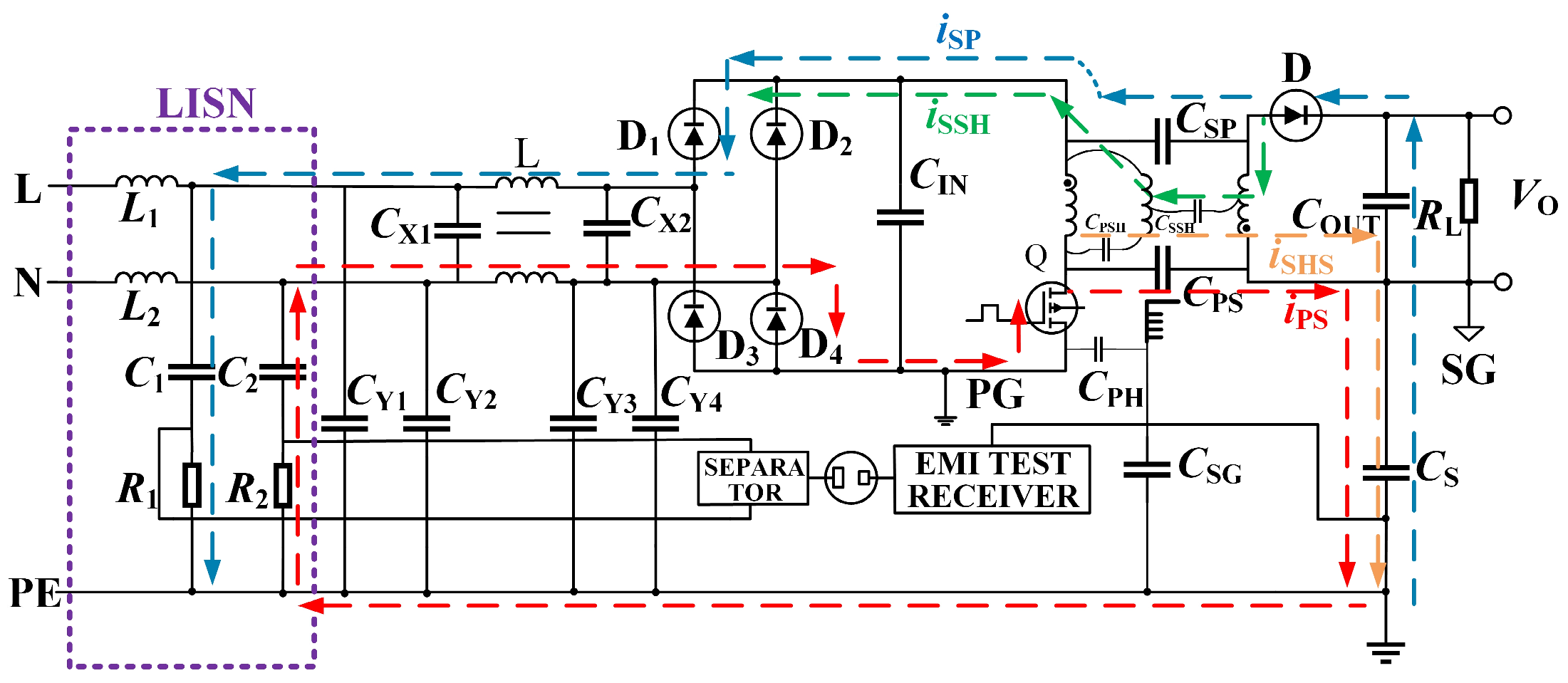
2. Transmission Mechanisms of Conducted Common-Mode Noise

The conducted interference transmission model of the flyback converter is shown in Figure 1. The front dashed lines, L1, L2, C1, C2, R1, and R2, collectively form a Line Impedance Stabilization Network (LISN). This network ensures a stable impedance for accurately testing the conducted noise of the device under test and extracting clean power quality. CY1, CY2, CX1, CX2, and L constitute a simple primary EMI filter. CX1 and CY2 filter out differential-mode interference between the grids. CY acts as a common-mode capacitor, and CY1, CY2, CY3, and CY4 are connected between a high voltage and the ground to filter out common-mode interference. Typically, ceramic capacitors of 4.7 nF and 2.2 nF are selected for this purpose. A separator is used to separate the differential-mode and common-mode noise, while an EMI receiver is utilized to receive the noise signal from the separator. D1, D2, D3, and D4 are the four diodes of the rectifier bridge. CIN is the input capacitance, COUT is the output capacitance, CPS is the primary noise source on the secondary-side winding’s equivalent capacitance, CSP is the secondary-side noise source on the primary winding’s equivalent capacitance, CPH is the distribution capacitance between the switching tubes and heatsink, CSG is the distribution capacitance of the heatsink with respect to the ground, and CS is the distribution capacitance of the secondary side with respect to the ground. VO is the output voltage, PE means the ground, PG means the transformer’s primary-side ground, and SG is the transformer’s secondary-side ground. For safety reasons, SG is generally directly connected to the ground.
Figure 2 shows the common-mode noise transfer path from the primary side of the transformer to the secondary side. In this scenario, noise originating from voltage jumps (VP) in the primary-side switching tube generates a noise current. This current flows through the primary equivalent capacitance (CPS) of the transformer, the secondary-side distributed capacitance relative to the ground (CS), and the LISN, forming a complete loop for noise transfer from the primary side to the secondary side.
Given that common-mode noise currents typically exhibit low magnitudes (in the μA range), the voltage drop across the LISN’s equivalent resistor is minimal and negligible compared to the noise source potential. The raw common-mode noise intensity for this path (without filtering) can be described by the following equation:
i CM 1 = ( C PS C S ) C PS + C S d u P d t
Figure 3 shows the common-mode noise transmission path from the secondary side of the transformer to the primary side. Here, noise originating from potential jumps in the secondary-side diode generates a noise current. This current traverses various components, including the secondary equivalent capacitance (CSP) of the transformer, the output capacitance (COUT), the secondary-side distributed capacitance relative to the ground (CS), and the LISN, forming a complete noise transmission loop from the secondary side to the primary side.
The raw common-mode noise intensity, iCM2, (without filtering) in this pathway can be calculated using the following equation:
i CM 2 = ( C SP C S ) C SP + C S d u D d t
The effect of the output capacitance (COUT) is not considered in Equation (2) because the capacitive reactance of COUT is significantly lower than that of CSP within the frequency range of 150 kHz to 30 MHz, which is used for evaluating conducted electromagnetic interference (EMI). Consequently, COUT has minimal impact on the common-mode noise in this pathway.
As shown in Figure 4, the transmission path of the common-mode noise, iCM3, involves a heatsink. Here, noise arising from voltage jumps (VP) in the primary-side switching tube generates a noise current. This current flows through the distributed capacitance of the heatsink (CPH), the distributed capacitance of the heatsink relative to the ground (CSG), and the LISN, forming a complete noise transmission loop.
The raw common-mode noise intensity, iCM3, (without filtering) in this method can be calculated using the following equation:
i CM 3 = ( C PH C SG ) C SP + C SG d u P d t
In an actual engineering environment, when the leakage current permitted by safety regulations is less than 0.35 mA, the capacitance value of the applied capacitor is adjusted. Simultaneously, based on the current value on the main line inductor (3A), the inductance is chosen to be 19 mH. The upper and lower stages of the common-mode inductance, L, function as a common-mode choke. When the common-mode current flows through them, the interference current aligns with the common-mode current, creating a high-impedance characteristic that effectively suppresses the common-mode current. This plays a significant role in reducing common-mode noise in the circuit.
To further clarify the impact of conducted interference, the interference propagation path is equivalently simplified below. The equivalent circuit is shown in Figure 5: R1 is the 20 Ω equivalent impedance of the LISN, VC is the voltage on the LISN, VP is the equivalent voltage of the switching tube, VD is the equivalent voltage of the diode, iPS is the equivalent capacitance current of the primary-side noise source with respect to the secondary-side winding, and iSP is the equivalent capacitance current of the secondary-side noise source with respect to the primary-side winding. Obviously, the common-mode displacement current will exist equally.

3. Conducted Common-Mode Noise Improvement Measures

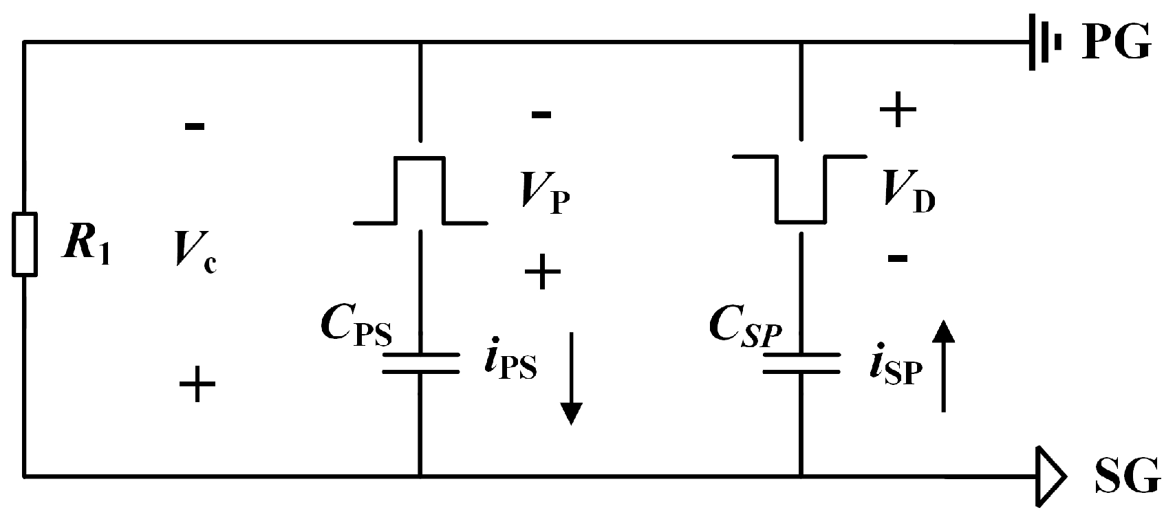
3.1. Compensation Capacitors Improve Noise Effects

To optimize the EMC performance of flyback power supplies, additional filter capacitors, especially Y capacitors for common-mode noise suppression, are usually introduced into the transformer’s primary and secondary circuits to mitigate the effects of the conducted noise. This principle involves measuring the actual noise current, iPS, on the primary side and the noise current, iSP, on the secondary side, then adjusting the impedance of the noise path according to the measured values by repositioning the added capacitor compensation accordingly to suppress common-mode noise generation. If the primary noise, iPS, increases, the capacitor, CY5, across the primary and secondary edges is placed on top of the transformer winding, and the secondary impedance is lowered by CY5 to increase iSP.
i SP = ( C SP + C Y 5 ) d V P d t
The secondary noise current increases with the increase in the secondary impedance. When the secondary noise is similar to the primary noise, the common-mode noise of the primary and secondary sides cancels each other out. As a result, the common-mode current flowing through the LISN impedance network decreases. Therefore, if the secondary noise, iSP, is larger, the compensation capacitor, CY6, should be placed in the opposite direction. At this time, the primary-side impedance decreases, and the value of iPS increases accordingly.
i PS = ( C PS + C Y 6 ) d V D d t
The total common-mode noise is iCM = iPSiSP. When the primary and secondary noises are equal, the conducted common-mode noise can be suppressed from the source. Based on the filtering theory, we can initially estimate the capacitance value of the Y capacitor. Under rational conditions, assuming that the maximum allowable ripple voltage is ΔV, the capacitor needs to provide a charge in one switching cycle equal to the charge change of the input current ripple, Irip, in that cycle, and according to the basic capacitor charging and discharging principle, the capacitance calculation formula is as follows:
C = I rip × T Δ V
where Irip is the desired common-mode noise current ripple, T is the operating period of the switching power supply, and ΔV is the maximum common-mode noise voltage fluctuation allowed on both sides of the capacitor. Experimental investigations on various values of compensation capacitance suggest an optimal range of 5 pF to 10 pF. If the value of the compensation capacitance is too small, the compensation effect may not be significant. Conversely, if the compensation capacitance is too large, it may result in overcompensation, leading to a deterioration in the common-mode noise suppression effect. The circuit model with a compensation capacitor added is shown in Figure 6.

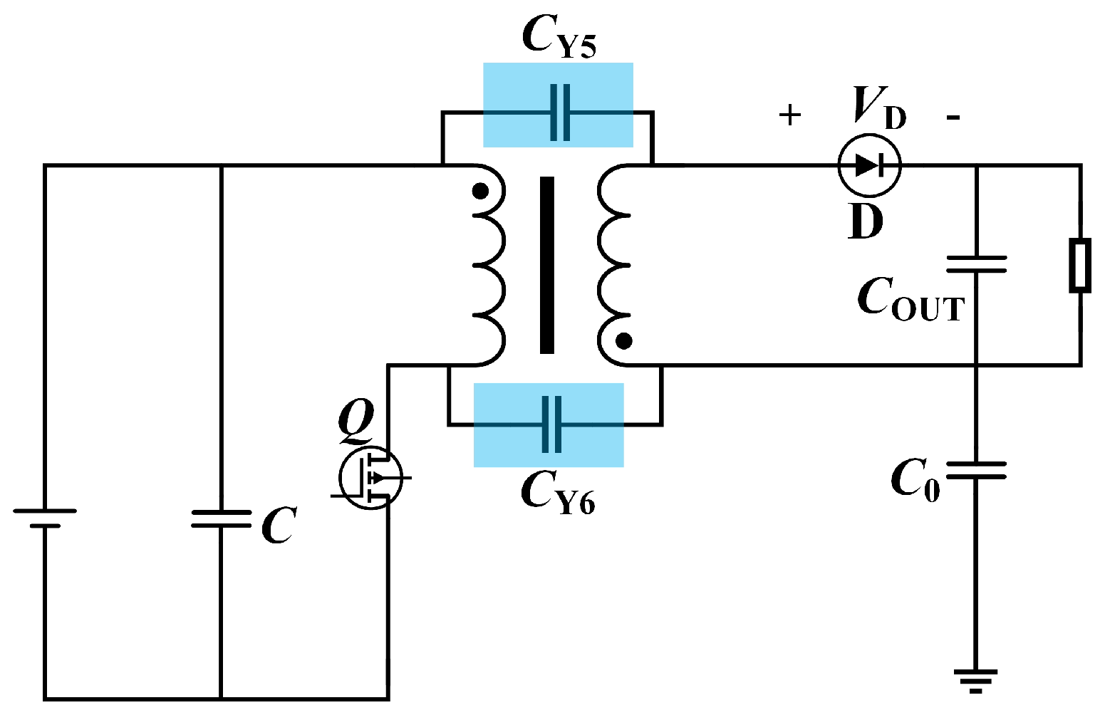
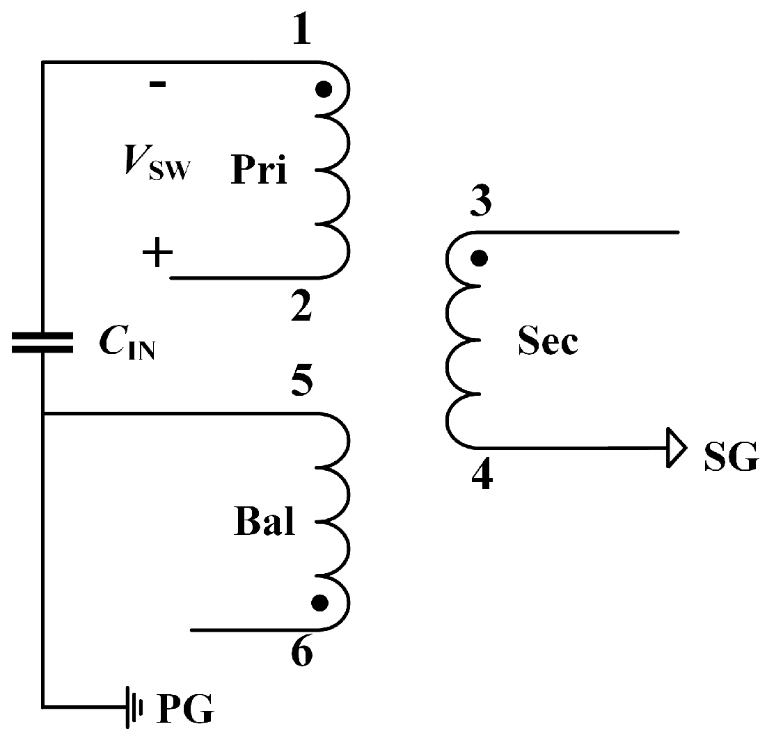
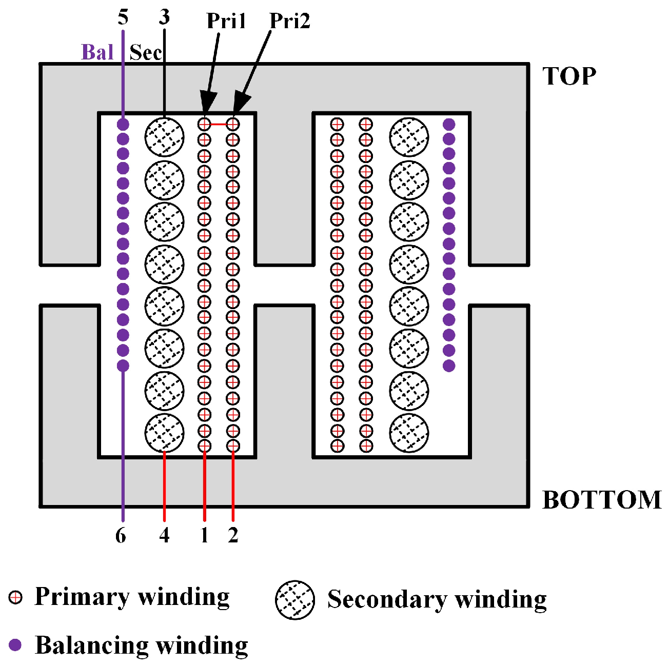
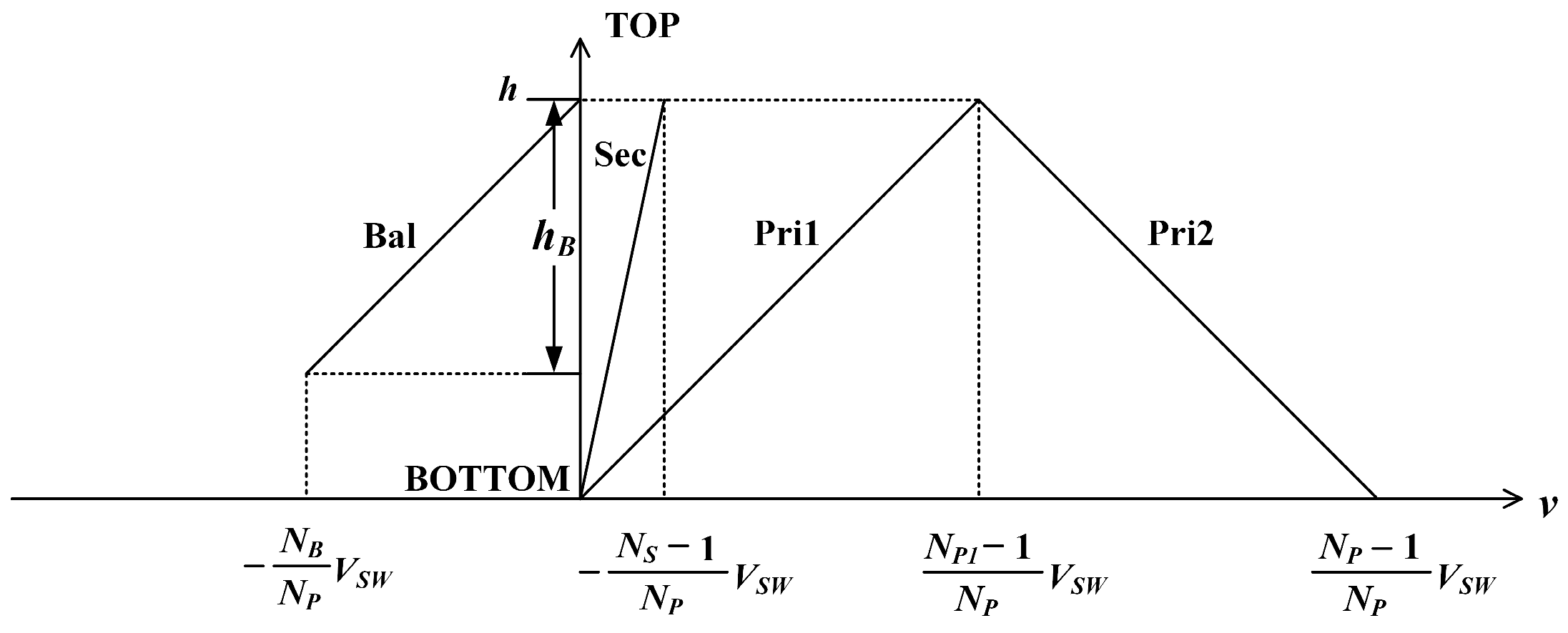
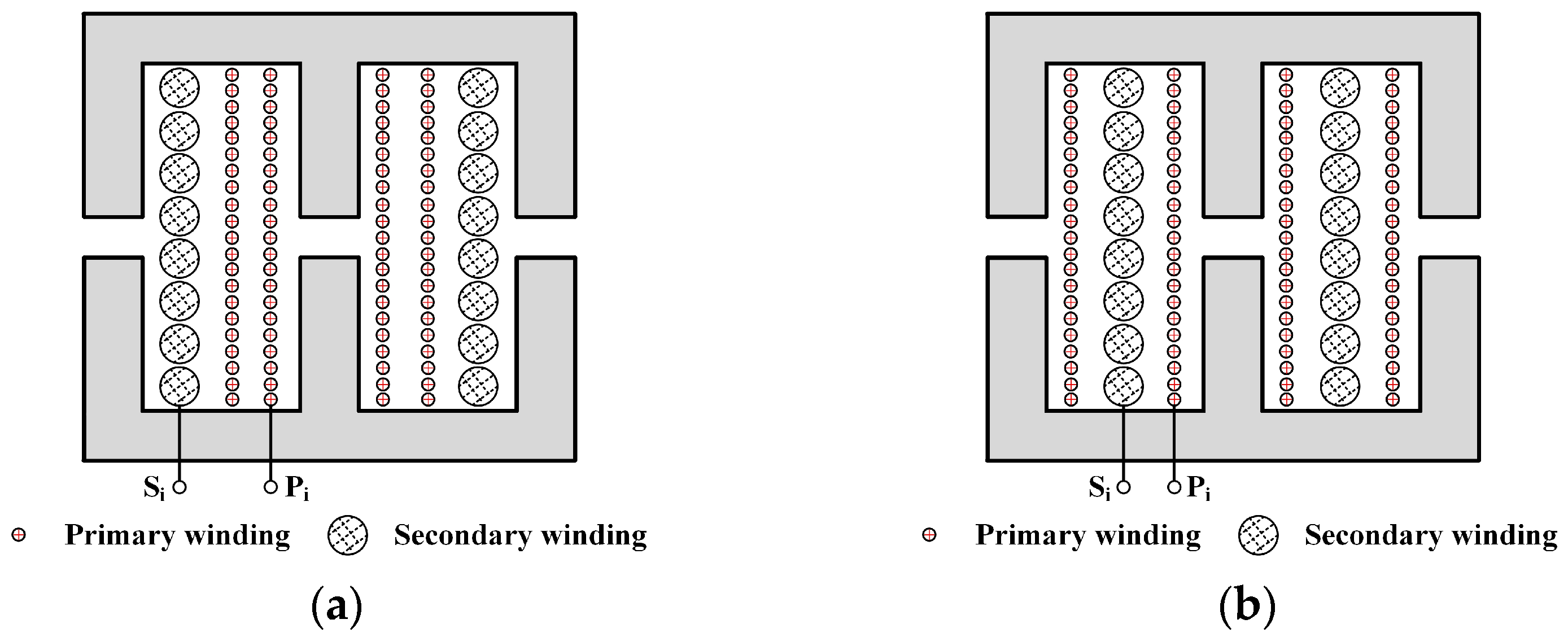
3.2. Balanced Winding Improves Noise Impact

The high-frequency switching characteristics of GaN devices lead to an asymmetric distribution of current in the circuit. The current conversion between the primary and secondary windings of the transformer, combined with the transformer’s leakage inductance and other parasitic parameters, unavoidably generates common-mode noise. To mitigate these issues, balanced windings are added to the transformer’s primary side to compensate for and suppress the noise. When the common-mode noise current passes through the power line, the balanced winding senses this noise and generates a reverse displacement current. This reverse displacement current creates a magnetic field in the core that cancels out the magnetic field of the original common-mode noise, significantly reducing the propagation of common-mode noise on the power line and greatly enhancing the EMI performance of the power system.
The transformer circuit model with a balanced winding added is shown in Figure 7. In this model, Pri denotes the primary winding, Sec denotes the secondary winding, and Bal denotes the balanced winding. VSW represents the voltage across the original primary winding, and Pri1 and Pri2 refer to two single-layer primary windings connected in series with turn numbers NP1 and NP2, respectively. In the actual design, the balanced winding is closely surrounded by the outer secondary winding, and its heterodyne end is connected to the primary ground (PG) of the transformer. This ensures that the transformer’s original noise can be canceled out with the common-mode noise transmitted from the secondary winding to the balanced winding. The winding arrangement of the transformer with the balanced winding added is shown in Figure 8.
By disregarding the leakage flux phenomenon and ignoring the AC impedance changes caused by the skin effect and proximity effect, we can assume that the potential is uniformly distributed in the winding, and the parasitic capacitance is also uniformly distributed along the winding. Referring to the layout of the winding arrangement and its endpoint connection relationship shown in Figure 8, we can plot the potential distribution of the winding at x = 0 along the y-axis, as shown in Figure 9. Here, h represents the height of the core window, l is the length of one turn of the winding, NB is the number of turns in the balanced winding, and hB is the width of the balanced winding.
From the winding potential distribution relationship shown in Figure 9, the potential expression for the primary winding, Pri1, is L x , y , and the potential expression for the secondary winding, Sec, is Q x , y :
Q x , y = N S 1 N P y h V SW + 1 N P x l V SW
L x , y = N P 1 1 N P y h V SW + 1 N P x l V SW
The common-mode displacement current, iPri1_Sec, from the primary winding, Pri1, to the secondary winding, Sec, can be derived using Equation (9), where CP1_S is the parasitic capacitance between the primary winding, Pri1, and the secondary winding, Sec, and dP1_S is the distance between the primary winding, Pri1, and the secondary winding, Sec.
i Pri 1 _ Sec = 0 h 0 l C P 1 _ S h l d d t L x , y Q x , y d x d y
C P 1 _ S ε h l d P 1 _ S
The expression for the potential of the balanced winding can be calculated from Equations (7)–(10) as follows:
N x , y = N B N P y h V SW N B N P h h V SW + 1 N P x l V SW
The common-mode displacement current, iSec_Bal, from the secondary winding to the balance winding can be determined using Equation (12), where CS_B is the parasitic capacitance between the secondary winding and the balance winding, dS_B is the distance between Sec and Bal, dB is the diameter of the balance winding, and ε is the dielectric constant.
i Sec _ Bal = h h B h 0 l C S _ B h B l d d t Q x , y N x , y d x d y
C S _ B ε h B l d S _ B
N B h B d B
Based on Formulas (7)–(14), and making iPri1_Sec = iSec_Bal, a numerical solution can be found by determining the number of turns in the balanced winding.

3.3. Transformer Structure Improves Noise Impact

Transformers play a crucial role in the electromagnetic compatibility (EMC) performance of power supplies. For flyback power supplies based on GaN devices, the noise generated by the high-frequency switching characteristics of GaN devices is superimposed on the noise produced by the transformer, affecting the EMI characteristics of the power supply. Therefore, it is necessary to implement improvement measures for the transformer. Elements such as the winding structure, winding sequence, and shielding form of the transformer significantly impact the electromagnetic interference (EMI) performance of the entire system. The distributed capacitance of the transformer is influenced by its structural parameters, and the size of the distributed capacitance between windings can be controlled by altering the winding structure and adding shielding layers to enhance the EMI performance of the flyback converter.
Parasitic resonance phenomena caused by the transformer’s interlayer capacitance pose a substantial challenge to the electromagnetic compatibility (EMC) performance of converters. To address these issues, the voltage and current stresses on switching tubes during switching are reduced by decreasing the interlayer capacitance, which in turn improves the transformer’s operating performance. Figure 10 shows the voltage distribution on the winding under four different winding methods (A, B, C, D). For the same winding, the inter-turn voltages of the two layers of the winding exhibit a decreasing trend, and the equivalent interlayer capacitance decreases accordingly.
Figure 11 shows the winding arrangement structure of the transformer using the ordinary winding method and sandwich winding method, respectively. Compared to the normal winding method, the sandwich winding method features a larger spacing between the two layers of primary windings, resulting in reduced interlayer capacitance. Consequently, the sandwich winding can diminish parasitic resonance in the circuit and mitigate the adverse effects of parasitic oscillations on the EMC performance of the converter.
Referring to Figure 11b, although the sandwich winding method decreases the interlayer capacitance, the increased area between the primary and secondary windings leads to an elevated intergroup capacitance. This increase in the intergroup capacitance exacerbates the common-mode noise of the transformer. To address this issue, a shielding layer can be added between the adjacent primary and secondary windings to reduce direct magnetic coupling, thereby effectively suppressing the propagation of common-mode noise.
When the flyback power supply operates at high frequencies, the common-mode noise generated by the high-speed switching of the transistors creates a strong electromagnetic field within the transformer. A sandwich-type winding structure can mitigate most of this noise by utilizing a shielding layer, which effectively guides the noise current to the ground, thereby eliminating conduction through the power line. Consequently, it significantly reduces electromagnetic interference with the external environment and the power grid.

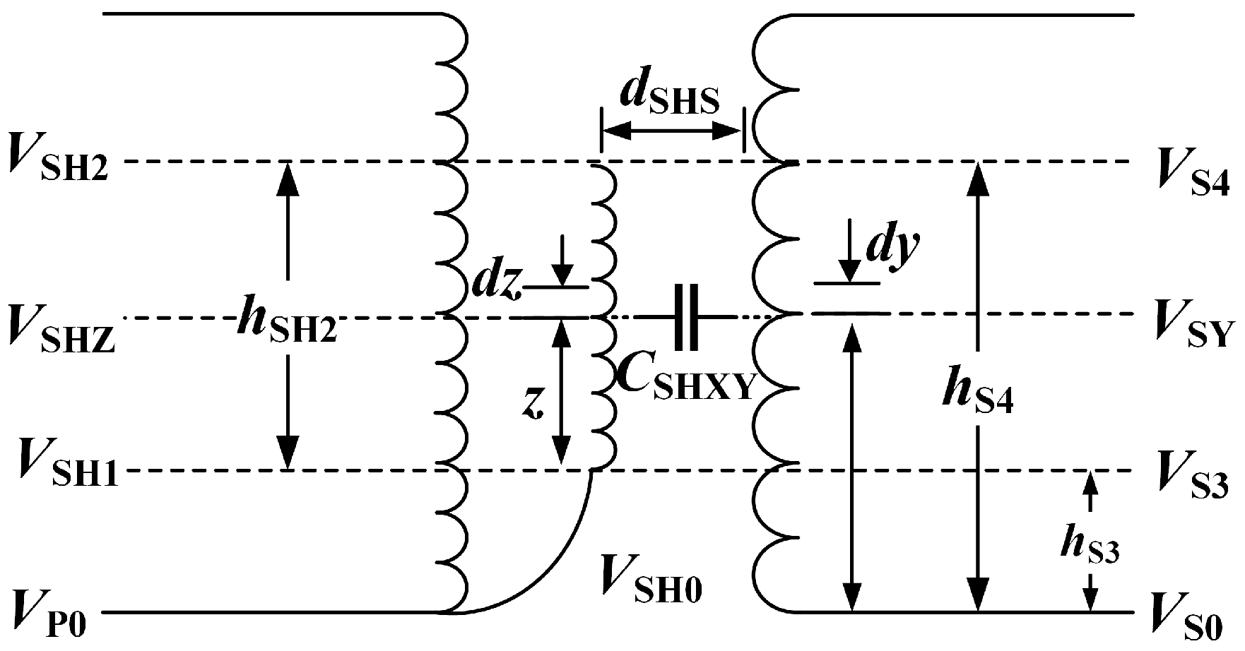
3.3.1. Transformer Distributed Capacitance Modeling

The common-mode noise transmission path with a shielding layer added is shown in Figure 12. This figure incorporates the path iSSH into the original common-mode noise transmission path. The noise is generated by a voltage jump, VP, in the primary-side switching tube, forming a noise current that flows through the distributed capacitance, CSSH, between the secondary winding and the shielding layer. It then passes through the rectifier bridge and the LISN, eventually returning to the diode, D, from the ground. Figure 13 shows an equivalent model of conducted interference with a shielding layer added.
The shielding layer can be categorized into two forms: copper foil shielding and winding shielding. Figure 14 shows the two forms of transformer shielding.
During the production process, it is crucial to prevent short circuits caused by overlapping copper foil. This can be achieved by properly wrapping insulating tape at the beginning and end of the foil. Enameled wire with diameters ranging from 0.1 mm to 0.3 mm is commonly used for shielding windings, as it helps maintain consistency in wire diameter and simplifies the manufacturing process. The number of turns and layout of the shielding winding significantly impact the overall shielding efficiency. Therefore, during fine winding operations, it is essential to use insulating tape to ensure robust and effective insulation at the winding ends. In summary, compared to relying solely on copper foil for shielding, the shielding winding design offers more advantages in terms of production convenience and cost control.
When exploring the practical engineering applications of sandwich-structure transformers, the winding point of the shielded winding is a critical yet often overlooked detail. The arrangement order of the windings is as follows: primary winding I, secondary winding, shielding winding, and primary winding II. The starting position of the shielded windings directly affects the transformer’s EMI characteristics. During the specific implementation process, the shielding winding should be wound from the transformer’s reference ground potential (RGP), with its end connected to the magnetic core. This connection strategy is significant as it ensures that during the transformer’s operation, the core and the winding’s voltages change in opposite directions, achieving a mutual offset effect and maximizing the core’s shielding effectiveness (the drain winding refers to the winding connected to the switching device). However, if the polarity of the shielding winding is misconfigured (i.e., the start and end are reversed), the voltage change direction will align with that of the drain windings, resulting in a loss in the shielding effect in the core. The winding order of the sandwich-structure transformer and the correct winding points for the shielded windings are shown in Figure 15.

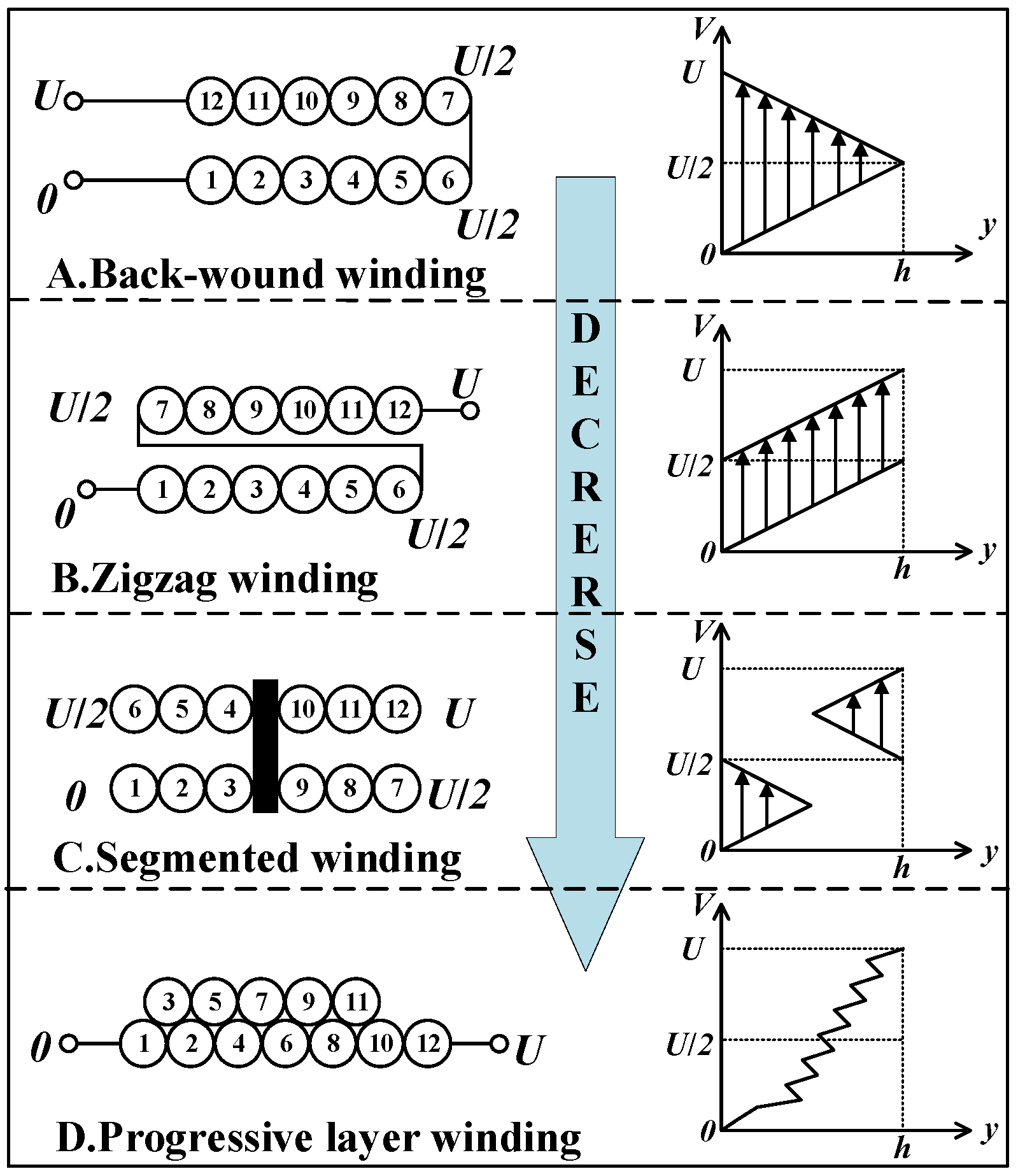
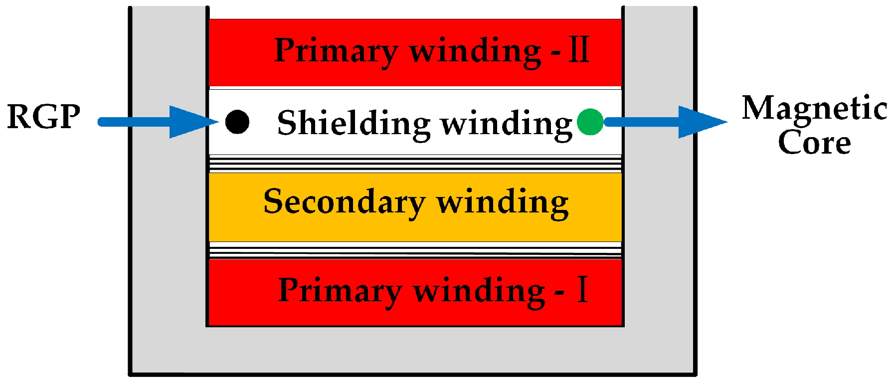
3.3.2. Shielding Winding Design for Flyback Transformers

According to the common-mode noise canceling principle of the flyback transformer, the optimal number of shielding winding turns can be determined by calculating the common-mode current and the number of winding turns. The complete inference steps are described below.
Figure 16 shows the common-mode interference transmission path with a shielding winding added. Here, iSHS represents the common-mode current transferred from the shielding winding to the secondary side, and iSSH represents the common-mode current transferred from the secondary side to the shielding winding.
The total common-mode current can be obtained from Figure 16 as follows:
i CM = ( i PS i SP ) + i SHS i SSH
where (iPSiSP) represents the common-mode current between the primary and secondary windings, and (iSHSiSSH) represents the common-mode current between the shielding and secondary windings.
The structure of the transformer windings significantly affects the magnitude of the common-mode current and the voltage distribution within the transformer. By utilizing the connections between the transformer windings, further calculations for the parameters (iPSiSP) and (iSHSiSSH) can be performed. Figure 17 shows the structural parameters between the primary and secondary windings of the transformer. Figure 18 shows the structural parameters between the shield winding and the secondary winding of the transformer.
VP0, VS0, and VSH0 denote the low-potential reference points on the primary, secondary, and shielding windings, respectively. hP1, hP1, and x represent the distances from a point on the original edge to the low-potential point. VP1, VP2, and VPX are the voltages of the primary winding at heights hP1, hP2, and x from the low-potential reference point. hS1, hS2, hS3, hS4, and y denote the distances from a point on the secondary side to the low-potential reference point. VS1, VS2, VS3, VS4, and VSY represent the voltages on the secondary side at heights hS1, hS2, hS3, hS4, and y from the low-potential reference point. hSH1, hSH2, and z denote the distances from a point on the shielding winding to the low-potential reference point. VSH1, VSH2, and VSHZ denote the voltages on the shielding winding at heights hSH1, hSH2, and z from the low-potential reference point. dPS represents the distance from the primary winding to the secondary winding. dSHS represents the distance between the shield and the secondary winding. CPXSY represents the magnitude of the capacitance element between the primary winding and the secondary winding. CSHSY represents the magnitude of the capacitance element between the shield winding and the secondary winding. Assuming that the distributed capacitance between adjacent ends of the winding is uniformly distributed, we obtain the following:
C PXSY = C PS 0 h P 2 h P 1 × h S 2 h S 1 C SHSY = C shs 0 h SH 2 h SH 1 × h S 4 h S 3
VPN0 represents the voltage difference between the first and last terminals of the primary winding, VSN0 represents the voltage difference between the first and last terminals of the secondary winding, VSHN0 represents the voltage difference between the first and last terminals of the shielding winding, NP represents the number of turns on the primary winding, NS represents the number of turns on the secondary winding, and v represents the voltage increment for each turn on the winding. By considering these variables, the following relationship can be derived:
V PN 0 = N P × v V SN 0 = N S × v V SHN 0 = N SH × v
The heights of the primary winding, secondary winding, and shielding winding are denoted as HP, HS, and HSH, respectively. The following relationship can then be established:
d V PX d t = d V P 0 + x H P × N P × v d t d V SY d t = d V S 0 + y H S × N S × v d t d V SHZ d t = d V SH 0 + z H SH × N SH × v d t
Based on the structural parameters labeled in Figure 17 and Figure 18, and in conjunction with the current and voltage relationship in the capacitor, the following equation can be formulated:
i P = h S 1 h S 2 h P 1 h P 2 C PXSY d V PX V SY d t d x d y i SH = h S 3 h S 4 h SH 1 h SH 2 C SHSY d V SHZ V SY d t d z d y
By substituting Equation (18) into (19), we obtain the following:
i P = h S 1 h S 2 h P 1 h P 2 C PXSY d V P 0 V S 0 d t + x H P × N P d v d t y H S × N S d v d t d x d y i S H = h S 3 h S 4 h SH 1 h SH 2 C SHSY d V SH 0 V S 0 d t + z H SH × N SH d v d t y H S × N S d v d t d z d y
The values of d(VP0VS0)/dt, d(VSH0VS0)/dt, and dv/dt in Equation (20) are associated with the interference source. The relationship between these values can be expressed as shown in Equation (21):
i P = h S 1 h S 2 h P 1 h P 2 C PXSY d V PX V SY d t d x d y i SH = h S 3 h S 4 h SH 1 h SH 2 C SHSY d V SHZ V SY d t d z d y
By substituting Equation (21) into Equation (20), the following relationship is obtained:
i P = C PS 0 d v d t × N 0 + h P 1 + h P 2 2 × H P × N P h S 1 + h S 2 2 × H S × N S i SH = C SHS 0 d v d t × N 1 + h SH 1 + h SH 2 2 × H SH × N SH h S 3 + h S 4 2 × H S × N S
CPS0 represents the intergroup distributed capacitance between the primary and secondary windings, while CSHS0 represents the intergroup distributed capacitance between the secondary and shielding windings. CPS0 and CSHS0 can be represented by the following equations:
C PS 0 = k PS ε PS h P 2 h P 1 × l avps d PS C SHS 0 = k SHS ε SHS h SH 2 h SH 1 × l avshs d SHS
Here, k represents a constant, ε represents the dielectric constant, and l represents the average circumference of the winding.

3.3.3. Determination of Optimum Number of Turns for Shielding Winding
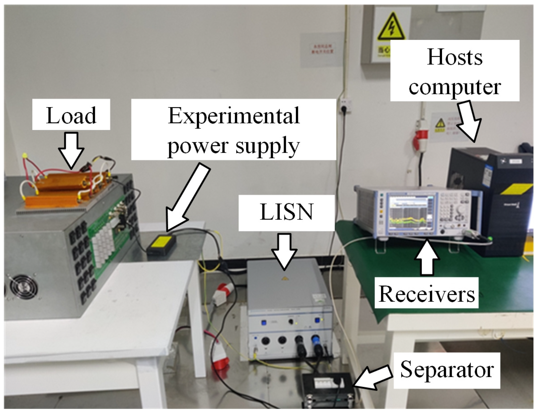
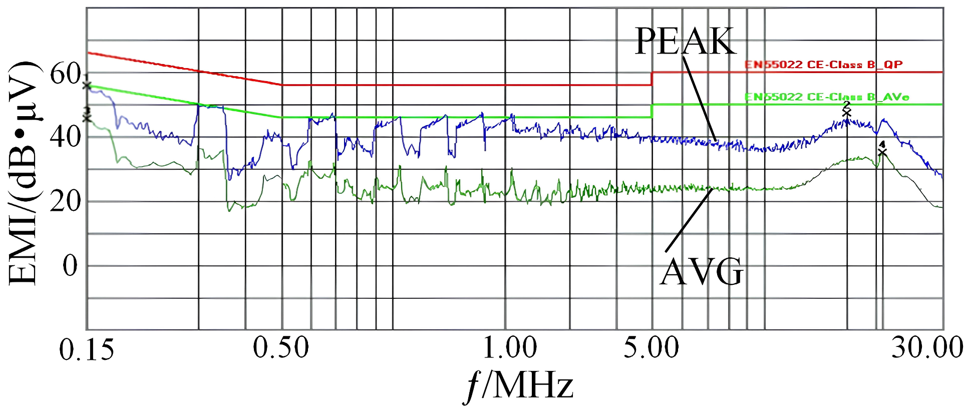
Given the overall architecture and materials of the transformer, the value of the structural capacitance depends solely on the number of turns on the shielding winding, NSH. There is a functional relationship between the common-mode current and the shielding winding, which can be represented as iCM = g(NSH) × dv/dt, where g(NSH) is a function of the number of turns on the shielding winding.
For any section of the transformer where the primary winding is adjacent to the secondary winding, the common-mode current, iP, between that adjacent section can be represented as follows:
i P = g P N SH × d v d t
g P N SH = k PS ε PS h P 2 h P 1 × l avps d PS N 0 + h P 1 + h P 2 2 × H P × N P h S 1 + h S 2 2 × H S × N S
Similarly, the common-mode current, i SH , between any section of the shielding winding and the secondary winding in the transformer can be represented as follows:
i SH = g SH N SH × d v d t
g SH N SH = k SHS ε SHS h SH 2 h SH 1 × l avshs d SHS N 1 + h SH 1 + h SH 2 2 × H SH × N SH h S 3 + h S 4 2 × H S × N S
HSH, hP1, hP2, hS1, hS2, hS3, and hS4 can be represented either by known transformer construction parameters or by a function, g(NSH), that depends on the number of turns on the shielding winding. This is shown in Equation (27), where wP represents the width of each turn on the primary winding, wS is the width of each turn of the primary winding, wSH is the width of each turn on the shielding winding, H0 is the height between the bottom end of the shielding winding and the bottom end of the primary winding, NP2 represents the number of turns on the winding with a corresponding height of hP2 in the primary-side winding, and NS2 represents the number of turns on the winding with a corresponding height of hS2 in the secondary winding.
H SH = w SH × N SH h P 1 = H 0 + w SH × N SH h P 2 = w P × N P 2 h S 1 = H 0 + w SH × N SH h S 2 = w S × N S 2 h S 4 = h S 3 + w SH × N SH
The total common-mode current in the transformer, as a function of the number of turns in the shielding winding, can be represented as follows:
i CM = j = 1 n i p j + k = 1 m i s h k = g N SH × d v d t
i p j represents the common-mode current in the region adjacent to the primary winding and the secondary winding in section j . n represents the number of segments in the transformer in which an adjacent region exists between the primary winding and the secondary winding. i s h k represents the common-mode current in the region adjacent to the shielding winding and the secondary winding in section k . m represents the number of segments in which an adjacent region exists between the shielding winding and the secondary winding.
Combined with Equation (29), when g N SH is at its minimum, the common-mode current, i CM , is also minimized. This can be solved by finding the root of g N SH = 0 . The optimum number of turns in the shielding winding can be obtained by taking the integer part of the root of g N SH = 0 .

4. Discussion

To validate the feasibility of the proposed conduction noise suppression method, a 150 W GaN flyback power supply was developed as the test subject, with its main parameters listed in Table 1. To ensure experimental accuracy, three noise reduction schemes (labeled as A, B, and C) were tested using a single experimental prototype. During these tests, only one component of the flyback power supply was altered at a time, such as adding a compensation capacitor, installing a balanced winding in the transformer, or installing a shielding winding in the transformer.
To validate the common-mode interference suppression method proposed in this paper, a conducted interference test platform was constructed in accordance with the CISPR 22 standard. The electrical connection block diagram of the experimental platform is shown in Figure 19. The experimental environment and noise testing instruments are shown in Figure 20. The LISN model used is the Cybertek EM5040B (by Shenzhen Zhiyong Electronics Co., Ltd., Shenzhen, China.), the EMI receiver model is the RS ESCI7 (by Rohde & Schwarz, Munich, Germany.), and the test frequency range is from 150 kHz to 30 MHz. The model of the separator is the TBLM1 MATE (by Satake, Hiroshima, Japan). During the testing process, the LISN was employed to eliminate power grid fluctuations and isolate the required signal, which was then transmitted to the EMI receiver via the separator. The EMI receiver performed spectral analysis on the received signal to obtain the noise spectrogram, which was subsequently transmitted to the host computer for processing and storage.
The EMI test was conducted on the original flyback power supply prototype without implementing the proposed noise reduction method. The transformer in the original flyback power supply prototype employs a standard winding technique, utilizing an EFD20 core model(by TDG, Zhejiang, China), and the core material is TP4 from TDG (Zhejiang, China). The EMI spectrum of the original flyback power supply is shown in Figure 21.
Scheme A: The experimental power supply in this scheme is based on the original flyback design, with an external compensation capacitor added. Figure 22 illustrates the EMI spectrum of the flyback power supply with a 5 pF compensation capacitor, while Figure 23 shows the EMI spectrum with a 20 pF compensation capacitor.
Comparing Figure 22 with the original EMI spectrogram, it is evident that the noise profile decreases by approximately 15 dB·μV in the 150 kHz to 1 MHz range and by about 10 dB·μV in the 1 MHz to 10 MHz range. The addition of appropriately valued compensation capacitors effectively reduces the common-mode noise level, particularly in the low- and mid-frequency bands of the noise spectrum, demonstrating a significant compensatory effect. This solution employs a simple circuit and is quick and effective to implement.
By comparing the test results in Figure 23 with the noise profile in Figure 22, it is evident that increasing the compensation capacitance from 5 pF to 20 pF results in a rise of approximately 20 dB·μV in the noise profile within the 4.5 MHz to 5.5 MHz range, indicating a significant deterioration in the compensation effect. As the compensation capacitance increases, noise propagation is further exacerbated.
Scheme B: This experimental power supply is based on the original flyback power supply, with the addition of a balanced winding in the transformer. The specific parameters of the transformer are detailed in Table 2. Figure 24 shows the EMI spectrum of the transformer with the balanced winding added. Comparing the noise curve in Figure 24 with the original spectrum, it can be observed that the noise level of the converter decreases by approximately 15 dB·μV in the range of 150 kHz to 1 MHz and by about 20 dB·μV in the range of 10 MHz to 20 MHz. This analysis indicates that the balanced winding significantly suppresses common-mode noise in both low- and high-frequency bands.
Scheme C: The experimental power supply in this scheme is based on the original flyback power supply, with the transformer employing a sandwich winding method and an additional shielding winding. The specific parameters of this transformer are shown in Table 3. Figure 25 shows the EMI spectrum of the transformer with the sandwich structure and additional shielding winding. Comparing the noise curve in Figure 25 with the original noise spectrum, it is evident that the noise spectrum decreased by approximately 15 dB·μV in the range of 150 kHz to 1 MHz, 10 dB·μV in the range of 10 MHz to 20 MHz, and 20 dB·μV in the range of 10 MHz to 30 MHz. The high-frequency noise peaks are significantly attenuated. In summary, the addition of the shielding winding to the transformer significantly improved the full-frequency-band common-mode noise of the flyback converter. Compared with conventional solutions, this program can achieve full-band noise suppression to a certain extent.

5. Conclusions

Flyback power supplies utilize GaN devices to increase efficiency and power density. However, the high-frequency switching characteristics of GaN devices cause EMI problems, jeopardizing the stable performance of the power supply. This paper provides a detailed analysis of the noise transmission mechanism in GaN-based flyback converters and proposes three improvement schemes to address electromagnetic interference. Scheme A: Based on the characteristics of the noise circuit, an external compensation capacitor is used to improve the impedance of the noise path, allowing primary and secondary noise to cancel each other out. Scheme B: Introducing balanced windings in the transformer effectively reduces common-mode noise caused by transformer leakage inductance and parasitic parameters. Scheme C: To suppress electromagnetic interference at the source, a method involving changes to the transformer structure and the use of shielded windings is proposed, significantly reducing common-mode noise levels and enhancing the electromagnetic compatibility of the GaN-based flyback power supply. Finally, a comparative experiment was conducted using the GaN-based flyback power supply, and the experimental results fully verify the feasibility of the proposed conducted interference suppression methods.
In this paper, three novel improvement schemes are proposed to enhance noise suppression in GaN-based flyback power supplies, providing significant practical guidance for improving their EMI performance.

Author Contributions

Conceptualization, J.Y. and Y.Y.; methodology, J.Y. and H.W.; software, J.Y. and H.W.; validation, J.Y., H.W. and X.F.; formal analysis, M.L.; investigation, Y.Y.; resources, Y.Y. and H.W.; data curation, Y.Y.; writing—original draft preparation, J.Y. and Y.Y.; writing—review and editing, J.Y. and H.W.; visualization, H.W. and X.F.; supervision, H.W.; project administration, J.Y.; funding acquisition, J.Y. and M.L. All authors have read and agreed to the published version of the manuscript.

Funding

This research was funded by the Natural Science Foundation of Guangxi Province of China, grant number 2021GXNSFAA220038.

Data Availability Statement

Data are contained within the article.

Conflicts of Interest

Author Xueliang Fu and Mingtong Li were employed by the company Greatwall Power Supply Technology Co., Ltd. The remaining authors declare that the research was conducted in the absence of any commercial or financial relationships that could be construed as a potential conflict of interest.

References

  1. Kozak, J.P.; Barchowsky, A.; Hontz, M.R.; Koganti, N.B.; Stanchina, W.E.; Reed, G.F.; Mao, Z.H.; Khanna, R. An analytical model for predicting turn-ON overshoot in normally-OFF GaN HEMTs. IEEE J. Emerg. Sel. Top. Power Electron. 2020, 8, 99–110. [Google Scholar] [CrossRef]
  2. Li, F.; Wang, R.; Huang, H.; Ren, Y.; Liang, Z.; Ren, G.; Tao, P.; Sun, Z.; Sun, N.; Zhao, C.; et al. Temperature-dependent hot electron effects and degradation mechanisms in 650-V GaN-based MIS-HEMT power devices under hard switching operations. IEEE J. Emerg. Sel. Top. Power Electron. 2021, 9, 6424–6431. [Google Scholar] [CrossRef]
  3. Collings, W.; Nelson, T.; Sellers, A.; Khanna, R.; Courtay, A.; Jimenez, S.; Lemmon, A. Optimization algorithms for dynamic tuning of wide bandgap semiconductor device models. In Proceedings of the 2021 IEEE Applied Power Electronics Conference and Exposition (APEC), Phoenix, AZ, USA, 14–17 June 2021; pp. 2427–2433. [Google Scholar]
  4. Sun, J.; Li, J.; Costinett, D.J.; Tolbert, L.M. A GaN-based CRM totem-pole PFC converter with fast dynamic response and noise immunity for a multi-receiver WPT system. In Proceedings of the IEEE Energy Conversion Congress and Exposition, Detroit, MI, USA, 11–15 October 2020; pp. 2555–2562. [Google Scholar]
  5. Yao, J.; Li, Y.; Wang, S.; Huang, X.; Lyu, X. Modeling and reduction of radiated EMI in a GaN IC-based active clamp flyback adapter. IEEE Trans. Power Electron. 2021, 36, 5440–5449. [Google Scholar] [CrossRef]
  6. Zhuolin, D.; Dong, Z.; Tao, F. Modeling and Prediction of Electromagnetic Interference in SiC Motor Drive Systems. Trans. China Electrotech. Soc. 2020, 35, 4726–4738. [Google Scholar]
  7. Fei, C.; Yang, Y.; Li, Q.; Lee, F.C. Shielding technique for planar matrix transformers to suppress common-mode EMI noise and improve efficiency. IEEE Trans. Ind. Electron. 2018, 65, 1263–1272. [Google Scholar] [CrossRef]
  8. Huang, X.; Feng, J.; Lee, F.C.; Li, Q.; Yang, Y. Conducted EMI analysis and filter design for MHz active clamp flyback front-end converter. In Proceedings of the 2016 IEEE Applied Power Electronics Conference and Exposition, Long Beach, CA, USA, 20–24 March 2016; pp. 1534–1540. [Google Scholar]
  9. Fu, K.; Chen, W. Evaluation Method of Flyback Converter Behaviors on Common-Mode Noise. IEEE Access 2019, 7, 28019–28030. [Google Scholar] [CrossRef]
  10. Li, Y.; Wang, S.; Sheng, H.; Lakshmikanthan, S. Investigate and Reduce Capacitive Couplings in a Flyback Adapter With a DC-Bus Filter to Reduce EMI. IEEE Trans. Power Electron. 2020, 35, 6963–6973. [Google Scholar] [CrossRef]
  11. Bai, Y.; Yang, X.; Li, X.; Zhang, D.; Chen, W. A novel balanced winding topology to mitigate EMI without the need fora Y-capacitor. In Proceedings of the 2016 IEEE Applied Power Electronics Conference and Exposition(APEC), Long Beach, CA, USA, 20–24 March 2016; pp. 3623–3628. [Google Scholar]
  12. Hsieh, H.; Shih, S. Effects of transformer structures on the noise balancing and cancellation mechanisms of switching power converters. In Proceedings of the 2014 International Power Electronics Conference (IPEC-Hiroshima 2014—ECCE ASIA), Hiroshima, Japan, 18–21 May 2014; pp. 2380–2384. [Google Scholar]
  13. Hsieh, H.I.; Shih, S.F.; Wang, H.; Liao, Y.H. Novel techniques to reduce common-mode (CM) and mix-mode (MM) EMI noise emissions based on noise balance and cancellation. In Proceedings of the 2016 IEEE International Conference on Power and Energy (PECon), Melaka, Malaysia, 28–29 November 2016; pp. 145–149. [Google Scholar]
  14. Pahlevaninezhad, M.; Hamza, D.; Servansing, A.; Bakhshai, A.; Jain, P. An integrated EMI suppression Y-caps applicable to high frequency planar transformers in high power DC-DC converters used for electric vehicle. In Proceedings of the IECON 2012—38th Annual Conference on IEEE Industrial Electronics Society, Montreal, QC, USA, 25–28 October 2012; pp. 4246–4251. [Google Scholar]
  15. Chen, H.; Xiao, J. Determination of Transformer Shielding Foil Structure for Suppressing Common-Mode Noise in Flyback Converters. IEEE Trans. Magn. 2016, 52, 1–9. [Google Scholar] [CrossRef]
  16. Li, Y.; Zhang, H.; Wang, S.; Sheng, H.; Chng, C.P.; Lakshmikanthan, S. Investigating Switching Transformers for Common Mode EMI Reduction to Remove Common Mode EMI Filters and Y-Capacitors in Flyback Converters. IEEE J. Emerg. Sel. Top. Power Electron. 2018, 6, 2287–2301. [Google Scholar] [CrossRef]
  17. Fu, K.; Chen, W.; Lin, S. A General Transformer Evaluation Method for Common-Mode Noise Behavior. Energies 2019, 12, 1984. [Google Scholar] [CrossRef]
  18. Guangdong, D.; Fanghua, Z. Research on Common Mode Conducted Noise Cancellation Method in Flyback Converter With Noise Balance Principle. Proc. CSEE 2019, 39, 3320–3327. [Google Scholar]
  19. Liu, Y.; Dong, G.; Zhang, F. Common Mode Noise Suppression in Flyback Converters. Trans. China Electrotech. Soc. 2019, 34, 4795–4803. [Google Scholar]
  20. Chan, Y.P.; Pong BM, H.; Poon, N.K.; Liu, J.C.P. Common-mode noise cancellation in switching-mode power supplies using an equipotential transformer modeling technique. IEEE Trans. Electromagn. Compat. 2012, 54, 594–602. [Google Scholar] [CrossRef]
  21. Xie, L.; Ruan, X.; Ye, Z. Equivalent noise source: An effective method for analyzing common-mode noise in isolated power converters. IEEE Trans. Ind. Electron. 2016, 63, 2913–2924. [Google Scholar] [CrossRef]
  22. Bai, Y.; Chen, W.; He, R.; Zhang, D.; Yang, X. EMI noise cancelation by optimizing transformer design without need for the traditional Y-capacitor. In Proceedings of the IEEE Applied Power Electronics Conference and Exposition, Long Beach, CA, USA, 20–24 March 2016; pp. 766–771. [Google Scholar]
  23. Kong, P.; Lee, F.C. Transformer structure and its effects on common mode EMI noise in isolated power converters. In Proceedings of the IEEE Applied Power Electronics Conference and Exposition, Palm Springs, CA, USA, 21–25 February 2010; pp. 1424–1429. [Google Scholar]
  24. Kang, B.G.; Chung, S.K.; Won, J.S.; Kim, H.S. EMI reduction technique of flyback converter based on capacitance model of transformer with wire shiel. In Proceedings of the 2015 9th International Conference on Power Electronics and ECCE Asia (ICPE-ECCE Asia), Seoul, Republic of Korea, 1–5 June 2015; pp. 163–169. [Google Scholar]
  25. Biela, J.; Kolar, J.W. Using Transformer Parasitics for Resonant Converters—A Review of the Calculation of the Stray Capacitance of Transformers. IEEE Trans. Ind. Appl. 2008, 44, 223–233. [Google Scholar] [CrossRef]
  26. Chen, H.; Zheng, Z.; Xiao, J. Determining the Number of Transformer Shielding Winding Turns for Suppressing Common-Mode Noise in Flyback Converters. IEEE Trans. Electromagn. Compat. 2018, 60, 1606–1609. [Google Scholar] [CrossRef]
  27. Fan, J.W.T.; Chow, J.P.W.; Chan, W.T.; Zhang, K.; Relekar, A.; Ho, K.W.; Tung, C.P.; Wang, K.W.; Chung, H.S.H. Modeling and experimental assessment of the EMI characteristics of switching converters with power semiconductor filters. IEEE Trans. Power Electron. 2020, 35, 2519–2533. [Google Scholar] [CrossRef]
Figure 1. Conducted interference transmission model of the flyback converter.
Electronics 13 02360 g001
Figure 2. Common-mode noise transmitted from the primary side to the secondary side of the transformer.
Electronics 13 02360 g002
Figure 3. Common-mode noise transmitted from the secondary side to the primary side of the transformer.
Electronics 13 02360 g003
Figure 4. Common-mode noise flowing through the heatsink.
Electronics 13 02360 g004
Figure 5. Conducted interference equivalent model.
Electronics 13 02360 g005
Figure 6. Circuit model with compensation capacitor added (CY5 or CY6).
Electronics 13 02360 g006
Figure 7. Transformer circuit model with balanced winding added.
Electronics 13 02360 g007
Figure 8. Winding arrangement of the transformer with balanced winding added.
Electronics 13 02360 g008
Figure 9. Winding potential distribution diagram (at x = 0).
Electronics 13 02360 g009
Figure 10. Different winding structures and their corresponding winding voltage differences.
Electronics 13 02360 g010
Figure 11. Winding arrangement structure corresponding to the two different winding methods for the transformer: (a) the ordinary winding method; (b) the sandwich winding method.
Electronics 13 02360 g011
Figure 12. Common-mode noise transmission path with shielding layer added.
Electronics 13 02360 g012
Figure 13. Equivalent model of conducted interference with shielding layer added.
Electronics 13 02360 g013
Figure 14. Two forms of transformer shielding layers: (a) transformer with copper foil shielding; (b) transformer with shielding winding.
Electronics 13 02360 g014
Figure 15. The order of the sandwich-structure transformer’s windings and the correct winding points for the shielding winding.
Electronics 13 02360 g015
Figure 16. Common-mode interference transmission path with shielding winding added.
Electronics 13 02360 g016
Figure 17. Structural parameters between the primary and secondary windings of the transformer.
Electronics 13 02360 g017
Figure 18. Structural parameters between the shield winding and the secondary winding of the transformer.
Electronics 13 02360 g018
Figure 19. Electrical connection block diagram of the experimental platform.
Electronics 13 02360 g019
Figure 20. Experimental environment and noise testing instruments.
Electronics 13 02360 g020
Figure 21. Original EMI spectrum.
Electronics 13 02360 g021
Figure 22. EMI spectrum with compensation capacitor added (5 pF).
Electronics 13 02360 g022
Figure 23. EMI spectrum with compensation capacitor added (20 pF).
Electronics 13 02360 g023
Figure 24. The EMI spectrum of the transformer with the balanced winding added.
Electronics 13 02360 g024
Figure 25. The EMI spectrum of the transformer with sandwich structure and additional shielding winding.
Electronics 13 02360 g025
Table 1. Electrical parameters of the prototype.
Electrical ParametersRating
Input voltage, V in / V 220
Output voltage, V o / V 12
Output power, P o / W 150
Switching frequency, f / Hz 1 × 10⁵
Table 2. Transformer parameters with balanced winding added.
Parameters (Units)Rating
NP (turns)120
NS (turns)9
h (mm)9.66
dP1_S (mm)0.325
dS_SH (mm)0.285
dP2_S (mm)0.452
dS_B (mm)0.325
dB (mm)0.200
Table 3. Transformer parameters with shielding winding added.
Parameters (Units)Rating
NP (turns)120
NS (turns)9
NSH (turns)40
hP1 (mm)8
hP2 (mm)8
hP3 (mm)6.28
wSH (mm)0.23
Disclaimer/Publisher’s Note: The statements, opinions and data contained in all publications are solely those of the individual author(s) and contributor(s) and not of MDPI and/or the editor(s). MDPI and/or the editor(s) disclaim responsibility for any injury to people or property resulting from any ideas, methods, instructions or products referred to in the content.

