Article

A Wideband Hybrid Envelope Tracking Supply Modulator with Slew-Rate-Enhanced Linear Amplifier

1
Institute of Astronautic Electronic Engineering, School of Aeronautics and Astronautics, Zhejiang University, Hangzhou 310027, China
2
Zhejiang Hangxinyuan IC Technology Co., Ltd., Hangzhou 310030, China
*
Author to whom correspondence should be addressed.
Electronics 2024, 13(14), 2701; https://doi.org/10.3390/electronics13142701
Submission received: 11 May 2024 / Revised: 1 July 2024 / Accepted: 3 July 2024 / Published: 10 July 2024

Abstract

:
A wideband hybrid envelope tracking supply modulator (HETSM) with a slew-rate-enhanced linear amplifier (LA) is described in this work. The proposed slew-rate enhancement (SRE) structure introduces a parallel auxiliary current path directly to the gate of the class-AB output stage, significantly accelerating the charging and discharging processes of the Miller capacitor without modifying the operating point of the remaining LA. The current delivered via this supplementary path shows a rapid increase, with changes in input voltage, culminating in diminished quiescent current levels. The supply modulator is fabricated in a 180 nm CMOS process. The measurement results show that HETSM is able to track a 100 MHz, 16QAM signal accurately, achieving the maximum efficiency of 87.4% at a 5.12 W output power, with a load that consists of a 5 Ω resistor and a paralleled 100 pF capacitor. The proposed LA realizes a slew rate of −1857/+1239 V / μ s and a bandwidth of 226.6 MHz under a 24 mA quiescent current.

1. Introduction

As the demand for data transmission rates continues to increase with modern communication technology, the increasing bandwidth and peak-to-average power ratio (PAPR) pose new challenges for the linearity and efficiency of power amplifiers. Envelope tracking (ET) technology is widely used, aiming to address this challenge by focusing on how to enhance the efficiency while ensuring the linearity of PAs [1,2,3,4]. Different from conventional power amplifiers with a fixed drain supply voltage, ET technology utilizes a dynamic drain voltage supply that tracks the envelope waveform [1]. As illustrated in Figure 1, where the green shaded region represents power losses on the power transistor, ET technology significantly reduces power dissipation on the power transistor, thereby improving efficiency [5,6,7,8]. HETSM, composed of switching converters (SWC) and LA and incorporating the advantages of both, has become the mainstream in research and applications and has been widely reported on in recent works [9,10,11,12,13,14,15,16,17,18,19].
For large bandwidth requirements, it becomes increasingly challenging for envelope tracking supply modulators to improve the bandwidth and slew rate while maintaining high efficiency [9,20,21]. Works in [22,23] proposed an envelope slew-rate reduction algorithm and demonstrated its beneficial effect on improving the linearity of ET PA. These works indicate the importance of meeting the signal slew-rate requirements for HETSM. Techniques such as adaptive biasing and super-class-AB recycling folded cascode are used to improve the slew rate without increasing the quiescent bias current in studies [20,24,25,26]. These techniques optimize the slew rate by amplifying the input-stage current during the transition state. Consequently, the large current needs to be transferred to the final stage via the front stages [9]. Works [9,27,28] introduced the auxiliary circuit injecting slew-rate-enhanced current, which is proportional to the input voltage of LA, to the gate of the output stage without increasing the input-stage current. However, the quiescent current of the auxiliary SRE circuit should be large to achieve a high slew rate.
In this work, a wideband HETSM with a slew-rate-enhanced LA is proposed. In the LA with SRE structures, a parallel auxiliary current path is introduced to the gate of the class-AB output stage, significantly accelerating the charging and discharging processes of the Miller capacitor without modifying the operating point of the remaining LA. The current delivered via this SRE path shows nonlinear characteristics, increasing sharply with changes in input voltage, thus reducing the quiescent current levels. The rest of this paper is organized as follows: Section 2 describes the principles and implementation of the recommended HETSM, including the LA with the proposed SRE structure. Measurement results are illustrated in Section 3, and the conclusion is summarized in Section 4.

2. Circuit Design

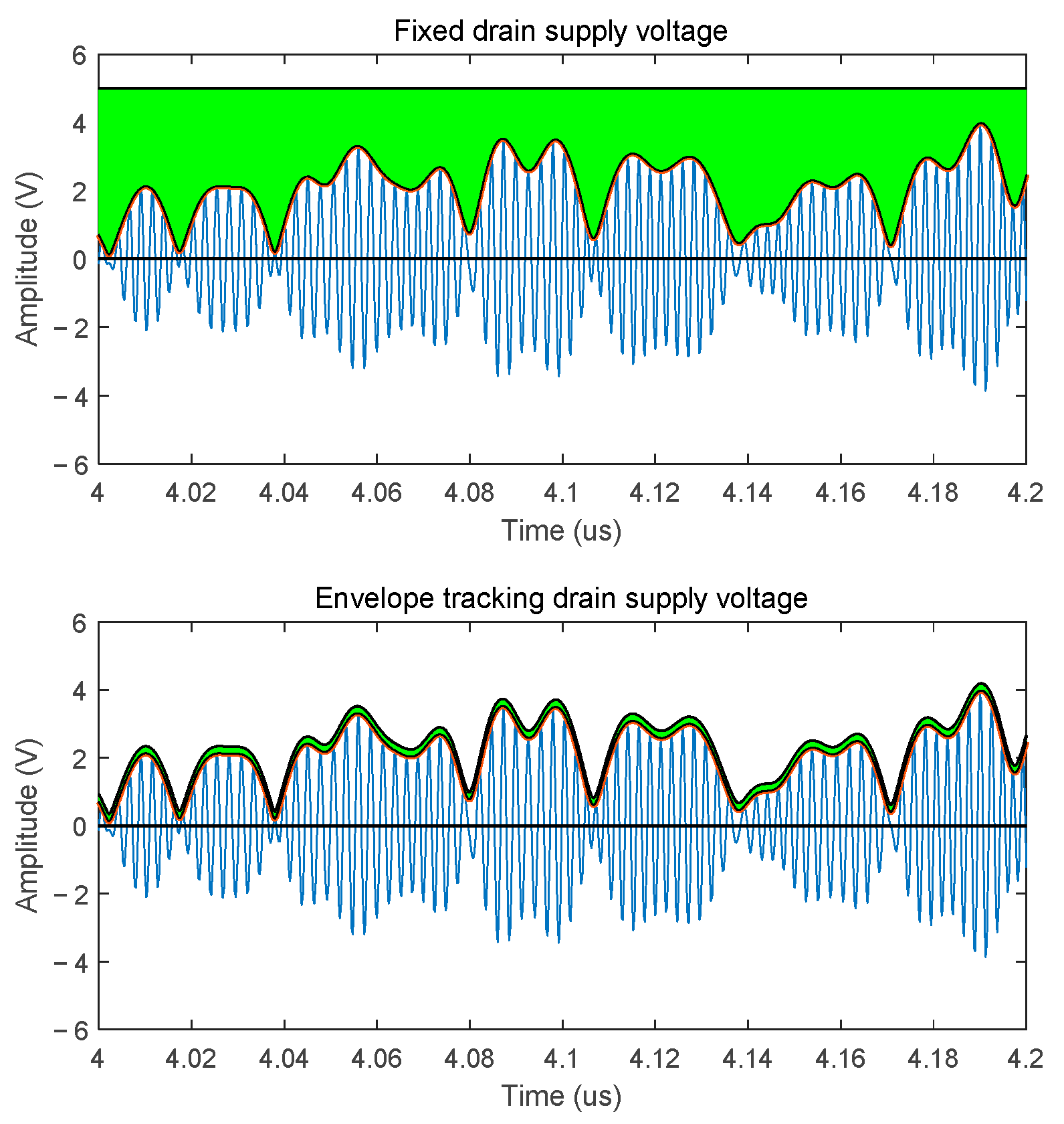
2.1. Principle of the HETSM System

As depicted in Figure 2, the recommended HETSM is composed of a high-efficiency SWC parallel with an LA, which has large unity-gain bandwidth (UGB). The high-efficiency SWC is responsible for delivering the primary power, catering to the low-frequency current demands of the PA [16]. Simultaneously, a high-speed, high-slew-rate LA precisely tracks the wideband envelope signal, ensuring the linearity of the PA load. The current of the LA’s output stage is mirrored out to generate the SW control (SW Ctrl) signal. Additionally, an external clock is used to control the frequency of the SWC, therefore controlling the efficiency of SWC. In this paper, the proposed HETSM is designed for GaAs Pas, which are powered by fixed drain voltages ranging from 4 V to 6 V. The paralleled 5 Ω resistor (RPA) and 100 pF capacitor (CPA) are utilized as the equivalent PA load for the LA [19,21].
Assuming that the HETSM system is to track a sinusoidal signal with amplitude A 0 and frequency f 0 , its expression is given in Equation (1):
f   ( t ) = A 0 s i n ( 2 π f 0 t )
Its derivative is shown as Equation (2). Therefore, theoretically, to track the signal f ( t ) , the slew rate needs to reach 2 π f 0 A 0 .
f ( t ) = 2 π f 0 A 0 cos ( 2 π f 0 t )
For a GaAs PA load, it is assumed that the maximum supply voltage of the adopted envelope tracking system is 6 V, and the minimum supply is 2 V. Theoretically, according to Equation (2), to track a sinusoidal signal with a peak-to-peak value of 4 V and a frequency of 100 MHz, the slew rate should ideally reach 1257 V / μ s . This value is not a practical guiding metric but a theoretical calculation because actual envelope signals are not pure sinusoids. However, it serves as a reference to estimate the required magnitude of the required slew rate.
In this work, a 100 MHz, 16QAM, and 8.49 dB PAPR signal is used for the test. The slew rate distribution of the corresponding envelope signal over a certain period is illustrated in Figure 3. It can be observed that for precise tracking of the envelope signal by the LA, its slew rate should at least exceed ± 800   V / μ s and preferably surpass ± 1000   V / μ s .
The consumption of the LA P L l o s s and the SWC P S W l o s s forms the consumption of the HETSM. The efficiency of the HETSM can be calculated as:
η = P o u t P o u t + P L l o s s + P S W l o s s = 1 1 + P L l o s s + P S W l o s s P o u t
For both P L l o s s and P S W l o s s , there is an intrinsic loss, no matter how small the output power is. For the LA, it is called quiescent dissipation, and for the SWC, it is called switching loss. Therefore, it is important to reduce the quiescent current of the LA to improve the efficiency of the HETSM.

2.2. LA Design with an SRE Structure

This paper proposed an LA design assisted by a nonlinear SRE structure, the diagram of which is shown in Figure 4. The nonlinear SRE structure is controlled by the input voltages, V I N P and V I N N , whose inputs are connected to nodes ① and ②. The input voltage difference, V I N P V I N N , is converted into nonlinear SRE currents, I S R P and I S R N , through the SRE structure. Due to the Miller compensation, the gates of the output transistors, nodes ③ and ④, become the slew-rate limiting points. Therefore, the output currents of the SRE structure, I S R P and I S R N , are then injected into nodes ③ and ④, accelerating the charging or discharging process of the Miller capacitors ( C 1 and C 2 ).

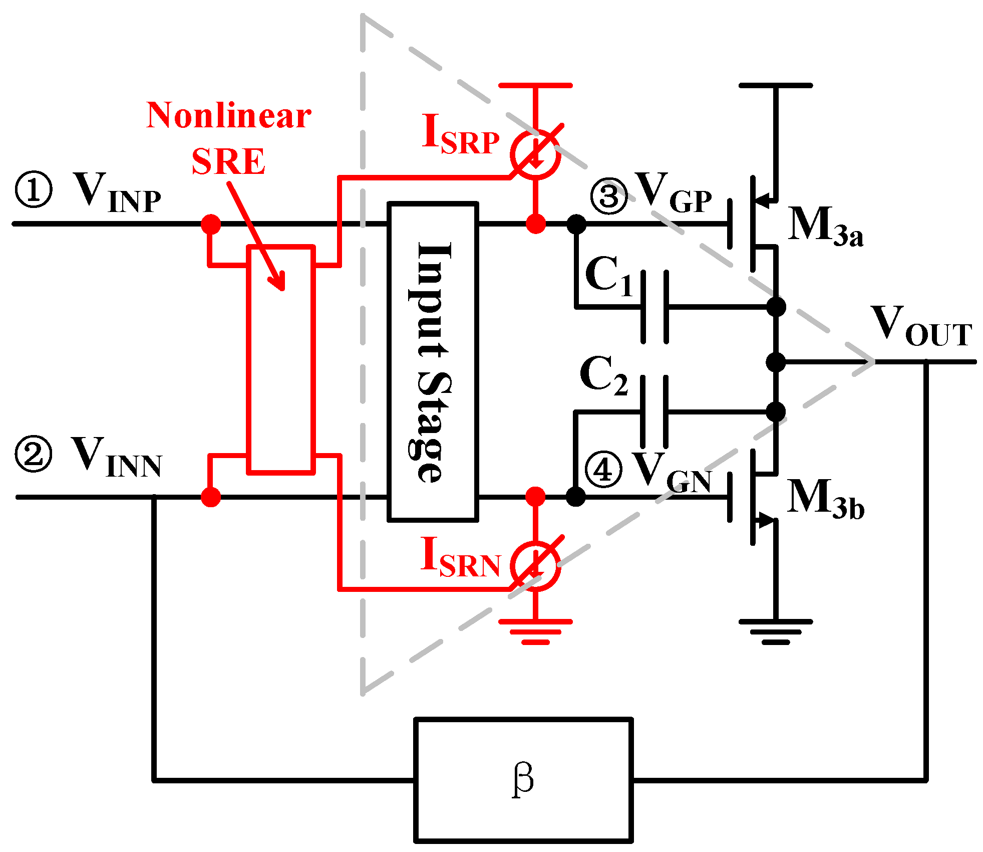
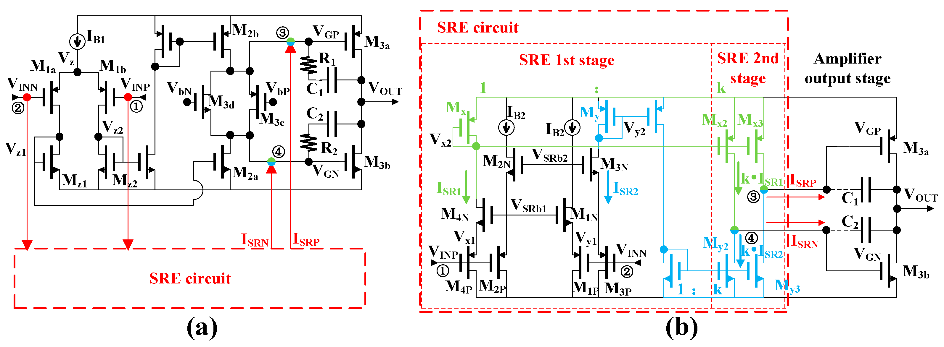
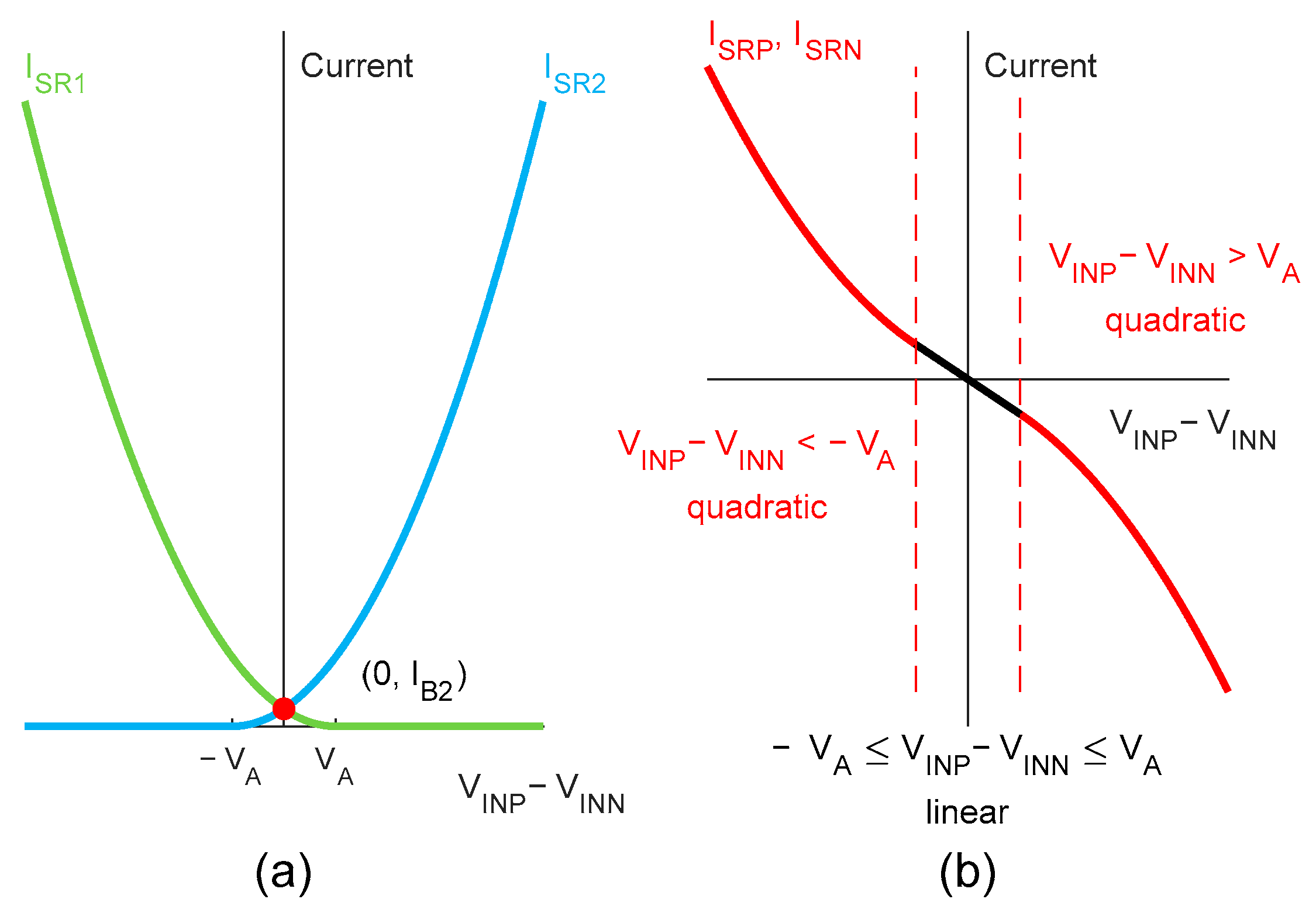
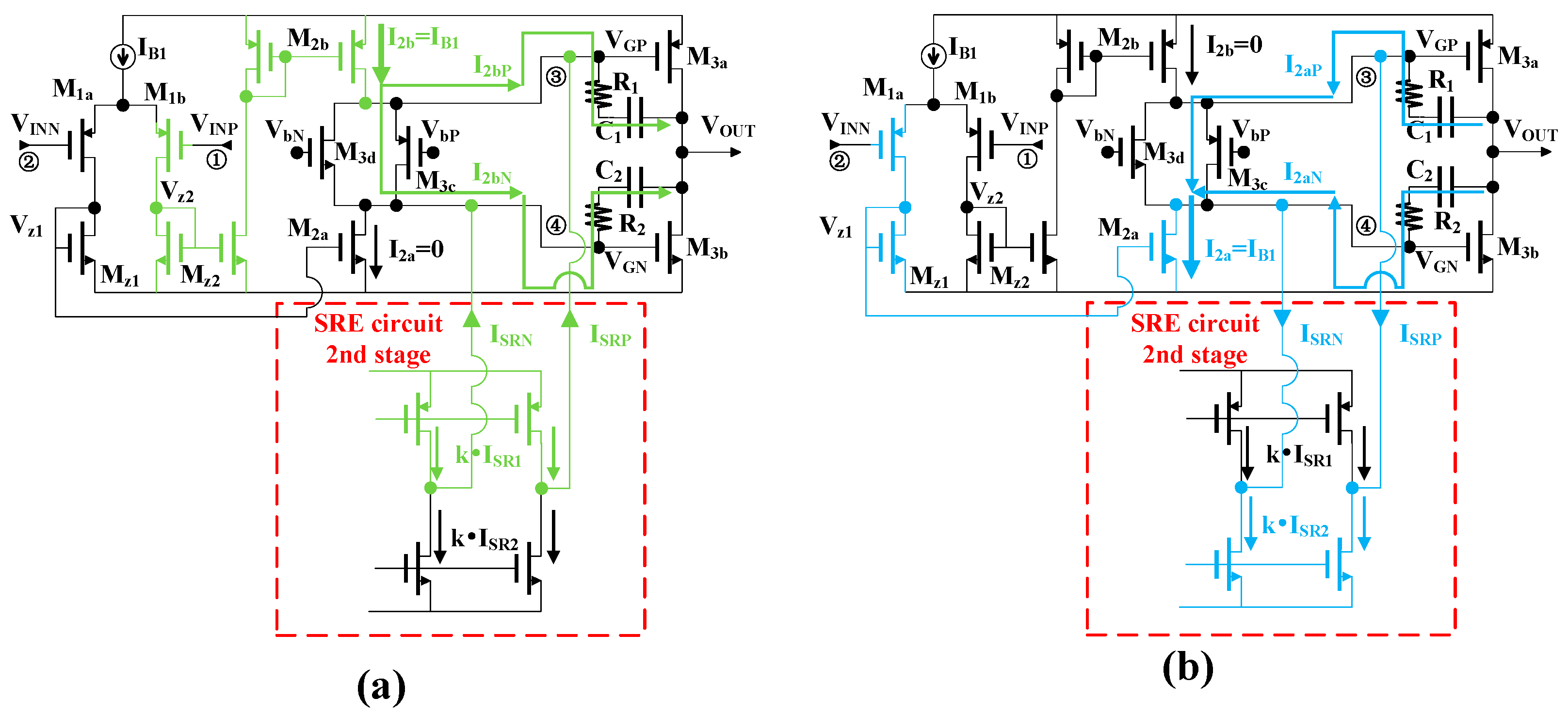
2.2.1. The Proposed SRE Circuit

Figure 5a depicts the overall circuit of the proposed LA with the SRE circuit, which corresponds to the diagram in Figure 4. Figure 5b illustrates the concrete SRE circuit.
In the first stage of the SRE circuit shown in Figure 5b, the input voltage difference, V I N P V I N N , is converted into the primary SRE currents, I S R 1 and I S R 2 , as demonstrated in the subsequent derivation.
For I S R 1 , it is determined by the dynamic bias voltage V S R b 1 and the input voltage V I N P , and the dynamic bias voltage V S R b 1 is determined by the fixed bias current I B 2 and the input voltage V I N N . By observing the branch circuit composed of transistors M 1 P and M 1 N , we can obtain Equation (4):
V S R b 1 = V I N N + | V G S 1 P | + V G S 1 N
where:
{ | V G S 1 P | = 2 I B 2 μ P C o x ( W / L ) 1 P + | V t h P | V G S 1 N = 2 I B 2 μ N C o x ( W / L ) 1 N + V t h N
In Equation (4) and the following equations, V G S i P and V G S i N are the gate-source voltages of transistors M i P and M i N , respectively; ( W / L ) i P and ( W / L ) i N are the aspect ratios of transistors M i P and M i N , respectively; μ P and μ N are the mobilities of electrons in PMOS transistors and NMOS transistors, respectively; V t h P and V t h N are the threshold voltages of PMOS transistors and NMOS transistors, respectively; and C o x is the gate oxide capacitance per unit area.
Similarly, by observing the branch circuit composed of transistors M 4 P and M 4 N , we can obtain Equation (6):
{ V S R b 1 = V I N P + | V G S 4 P | + V G S 4 N | V G S 4 P | = 2 I S R 1 μ P C o x ( W / L ) 4 P + | V t h P | V G S 4 N = 2 I S R 1 μ P C o x ( W / L ) 4 N + V t h N
Then, by substituting Equation (4) into Equation (6), we can figure out the expression of I S R 1 , as illustrated in Equation (7).
I S R 1 = 1 2 [ 1 1 μ P C o x ( W / L ) 4 P + 1 μ N C o x ( W / L ) 4 N ( V I N N V I N P + 2 I B 2 μ P C o x ( W / L ) 1 P + 2 I B 2 μ N C o x ( W / L ) 1 N ) ] 2
In this design, the dimensions of the transistors satisfy the relationships: ( W / L ) 1 P = ( W / L ) 2 P = ( W / L ) 3 P = ( W / L ) 4 P , and ( W / L ) 1 N = ( W / L ) 2 N = ( W / L ) 3 N = ( W / L ) 4 N . Therefore, we can simplify Equation (7):
I S R 2 = { 1 2 ( 1 1 μ P C o x ( W / L ) 1 P + 1 μ N C o x ( W / L ) 1 N ( V I N N V I N P ) + 2 I B 2 ) 2 , V I N P V I N N V A 0 , V I N P V I N N > V A
where V A denotes the threshold input voltage difference of the SRE circuit:
V A = 2 I B 2 μ P C o x ( W / L ) 1 P + 2 I B 2 μ N C o x ( W / L ) 1 N
It is worth noting that in Equation (8), when the condition V I N P V I N N V A is satisfied, transistors M 4 P and M 4 N are operating in the saturation region. Outside this range, the transistors M 4 P and M 4 N are cut off, and as a result, I S R 1 = 0 .
Similarly, we can derive the other primary SRE current, I S R 2 , as illustrated in Equation (10):
I S R 2 = { 1 2 ( 1 1 μ P C o x ( W / L ) 1 P + 1 μ N C o x ( W / L ) 1 N ( V I N P V I N N ) + 2 I B 2 ) 2 , V I N P V I N N V A 0 , V I N P V I N N < V A
According to the calculation results, the corresponding curves of the primary SRE currents, I S R 1 and I S R 2 , are drawn in Figure 6a. We can see, relative to the value of the quiescent bias current I B 2 , that the primary SRE currents can be very large when needed.
Then, in the second stage of the SRE circuit shown in Figure 5b, the primary SRE currents, I S R 1 and I S R 2 , are amplified k times by current mirrors. Subsequently, they are subtracted to yield the output SRE currents, I S R P and I S R N , as shown in Equation (11).
I S R P = I S R N = k ( I S R 1 I S R 2 )
By substituting Equations (8) and (10) into Equation (11), we obtain the complete expression of the output SRE currents:
I S R P = I S R N = { k 2 ( 1 1 μ P C o x ( W / L ) 1 P + 1 μ N C o x ( W / L ) 1 N ( V I N N V I N P ) + 2 I B 2 ) 2 , V I N P V I N N < V A 2 k 2 I B 2 1 μ P C o x ( W / L ) 1 P + 1 μ N C o x ( W / L ) 1 N ( V I N N V I N P ) , V A V I N P V I N N V A k 2 ( 1 1 μ P C o x ( W / L ) 1 P + 1 μ N C o x ( W / L ) 1 N ( V I N P V I N N ) + 2 I B 2 ) 2 , V I N P V I N N > V A
Therefore, we can draw the corresponding curve of the output SRE currents, I S R P and I S R N , respectively, in Figure 6b. When the slew rate of the input signal at node ① in Figure 5 is small, the input voltage difference, V I N P V I N N , is small. From Equation (12) and Figure 6b, we notice that when V I N P V I N N is small, which satisfies | V I N P V I N N | V A , the SRE currents, I S R P and I S R N , linearly increase with V I N P V I N N . Especially when V I N P V I N N = 0 , we have I S R P = I S R N = 0 . In this case, the SRE circuit does not modify the operating point of the remaining LA. When the slew rate of the input signal becomes large, the LA converts from the linear amplification state to the transition state, and the input voltage difference V I N P V I N N grows, due to the difficulty of input signal tracking. The corresponding SRE currents, I S R P and I S R N , will quadratically grow with the enlarged input voltage difference. These additionally injected SRE currents can effectively increase the slew rate of the output voltage while maintaining a low quiescent current level.
The operating conditions of the transistors and the current flow during the transition state are shown in Figure 7. When V I N P < V I N N , as shown in Figure 7a, the differential pair transistor M 1 a is turned off, and all of the tail current I B 1 flows through transistor M 1 b . Additionally, the current I 2 b running through transistor M 2 b reaches its maximum value I B 1 , while transistor M 2 a is turned off with no current passing through. The current I 2 b is split into two parts: I 2 b P charges compensation capacitor C 1 , and I 2 b N discharges compensation capacitor C 2 . Then, the gate voltages of the push–pull output stage’s transistors V G P (at node ③) and V G N (at node ④) increase, causing the output voltage V O U T to decrease. Because the change in V O U T is much greater than the changes in V G P and V G N , the charge and discharge rates of C 1 and C 2 will determine the slew rate of the output voltage V O U T . The proposed SRE circuit injects additional nonlinear SRE currents, I S R P and I S R N , into nodes ③ and ④, respectively, which effectively enhances the slew rate. When V I N P > V I N N , as illustrated in Figure 7b, a similar situation occurs.

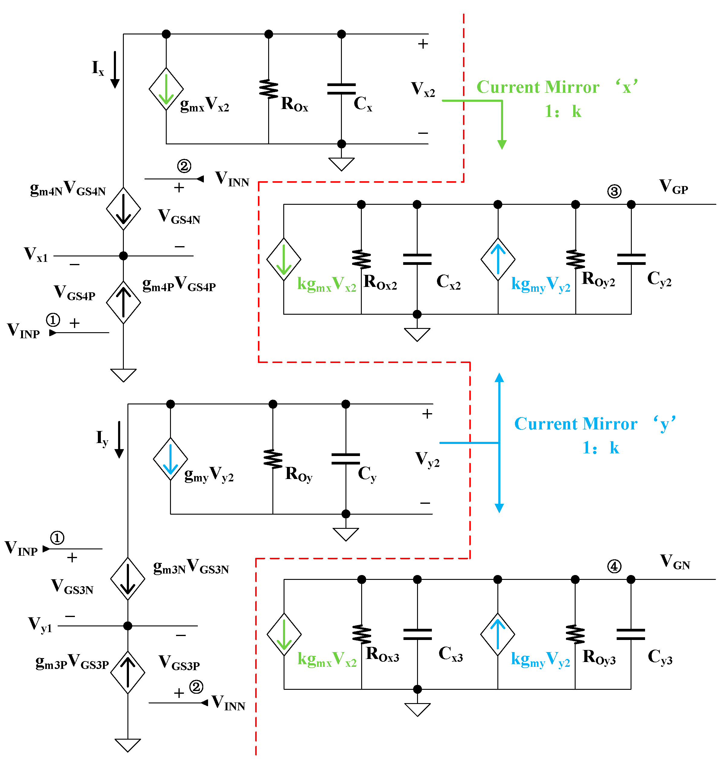
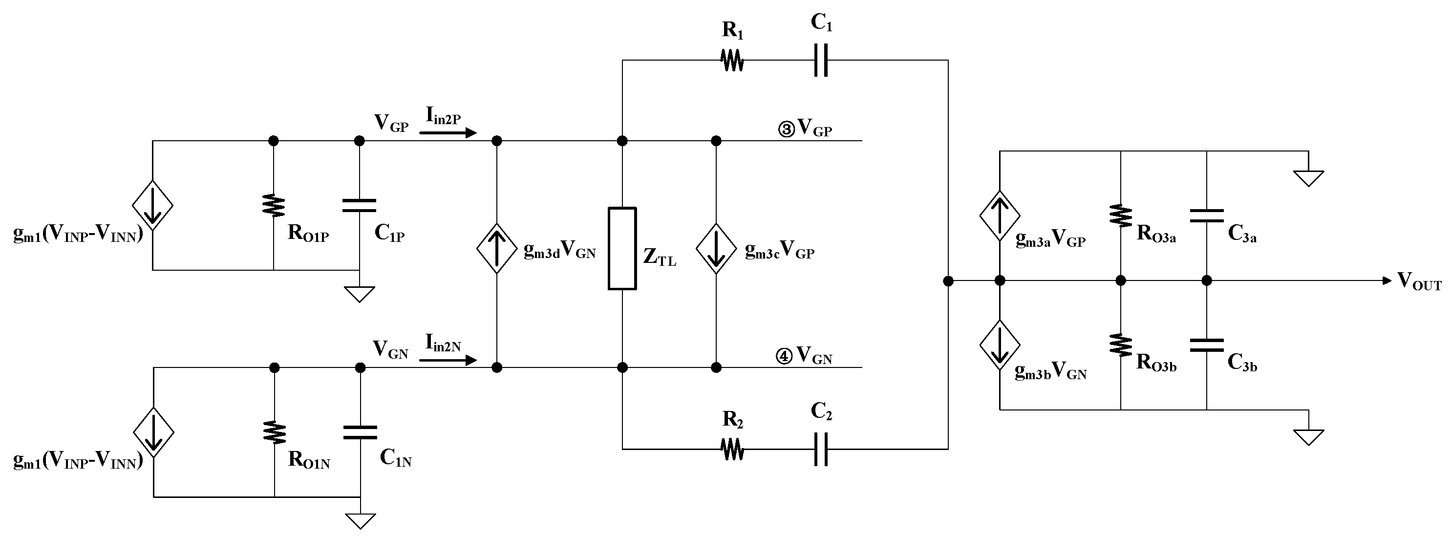
2.2.2. AC Analysis of the LA with the Proposed SRE Circuit

The SRE circuit in Figure 5b can be extracted to a corresponding small-signal model, as shown in Figure 8. In the small-signal models below, unless otherwise specified, g m i , R O i , and C i are used to represent the transconductance g m , output resistance r d s , and output capacitance C d of transistor M i , respectively, where i denotes the subscript of the transistor. Due to the symmetrical design of the circuit, we have g m 3 P = g m 4 P and g m 3 N = g m 4 N . The small-signal model in Figure 8 can be simplified to a one-stage amplifier model within the red dashed box in Figure 9. We can derive the relationship given in Equation (13):
{ g m S R = 2 k g m 3 P g m 3 N g m 3 P + g m 3 N R O S R P = R O x 2 | | R O y 2 , R O S R N = R O x 3 | | R O y 3 C S R P = C x 2 + C y 2 , C S R N = C x 3 + C y 3
The detailed derivation process of the small-signal LA model is provided in Supplementary Material.
As derived in Supplementary Material, we can combine the input stage of LA with the SRE circuit to simplify it into the first-stage amplification circuit model shown on the left side of Figure 10. We can derive the relationship shown in Equation (14):
{ g m 1 = g m S R + g m 1 C o n v = 2 k g m 3 P g m 3 N g m 3 P + g m 3 N + g m 1 a g m 1 b g m 1 a + g m 1 b R O 1 P = R O S R P | | R O 2 b , R O 1 N = R O S R N | | R O 2 a C 1 P = C S R P + C 2 b + C g s 3 a , C 1 N = C S R N + C 2 a + C g s 3 b
The small-signal model of the entire LA after the aforementioned simplification process is shown in Figure 10. If we incorporate the following steps into the LA design, we can achieve symmetry in the circuit to a large extent:
(1) Let k N P = R O 1 N R O 1 P .
(2) Select the sizes of M3a and M3b, such that   C 1 P = k N P C 1 N .
(3) Choose the R1/C1 and R2/C2 that satisfy the relation.
Specifically, when R O 1 N = R O 1 P , we have k N P = 1 . In this case, we derive that V G P V G N = 0 . When V G P = V G N , the effects of M 3 c and M 3 d cancel each other out because the current g m 3 d V G N is equal to the current g m 3 c V G P , as shown in Figure 10, and the current through the impedance Z T L equals zero.
Then, due to symmetry, the LA circuit can be simplified to that shown in Figure 11. We find that the small-signal model of the proposed amplifier can be simplified to the well-known two-stage operational amplifier model, simply by substituting the parameters with those in parentheses shown in Figure 11. We can derive the relationship shown in Equation (15):
{ g m I = 2 g m 1 = 4 k g m 3 P g m 3 N g m 3 P + g m 3 N + 2 g m 1 a g m 1 b g m 1 a + g m 1 b R I = R O 1 N | | R O 1 P = ( R O S R N | | R O 2 a ) | | ( R O S R P | | R O 2 b ) C I = C 1 P + C 1 N = ( C S R P + C 2 b + C g s 3 a ) + ( C S R N + C 2 a + C g s 3 b ) R c = R 1 | | R 2 , C c = C 1 | | C 2 g m II = g m 3 a + g m 3 b R II = R O 3 a | | R O 3 b , C II = C 3 a + C 3 b + C L
If the poles are widely spaced, then we can derive the expressions for the zeroes and poles as follows:
{ p 1 1 g m II R II R I C c p 2 g m II C II p 3 = 1 R z C I z 1 = 1 C c ( 1 / g m II R z )
In the AC analysis, the recommended SRE circuit is equivalent to a stage that is parallel to the input stage of the amplifier and can be integrated into the input stage circuit. Therefore, when selecting the compensation capacitor and resistor to adjust the stability of the amplifier, the impact of the SRE circuit must be considered.
In the recommended LA, the slew rate is determined by Equation (17):
S R = I B 1 + I S R P C 1
In the transition state, is much greater than the static current parameter I B 2 related to the SRE circuit. The recommended LA in our work can achieve a high slew rate with low quiescent power consumption.
The UGB of the proposed LA can be expressed as:
U G B g m I C c = ( 4 k g m 3 P g m 3 N g m 3 P + g m 3 N + 2 g m 1 a g m 1 b g m 1 a + g m 1 b ) 1 C 1 + C 2
Observing Figure 5, we can determine the expression of the quiescent current of the LA:
I Q = ( 2 I B 1 + I Q _ 3 a ) + ( 5 I B 2 + 2 kI B 2 )
where I Q _ 3 a is the quiescent current of the output stage.
Based on the design targets for UGB and the slew rate, through multiple iterations, we are seeking a design solution that minimizes quiescent power consumption.

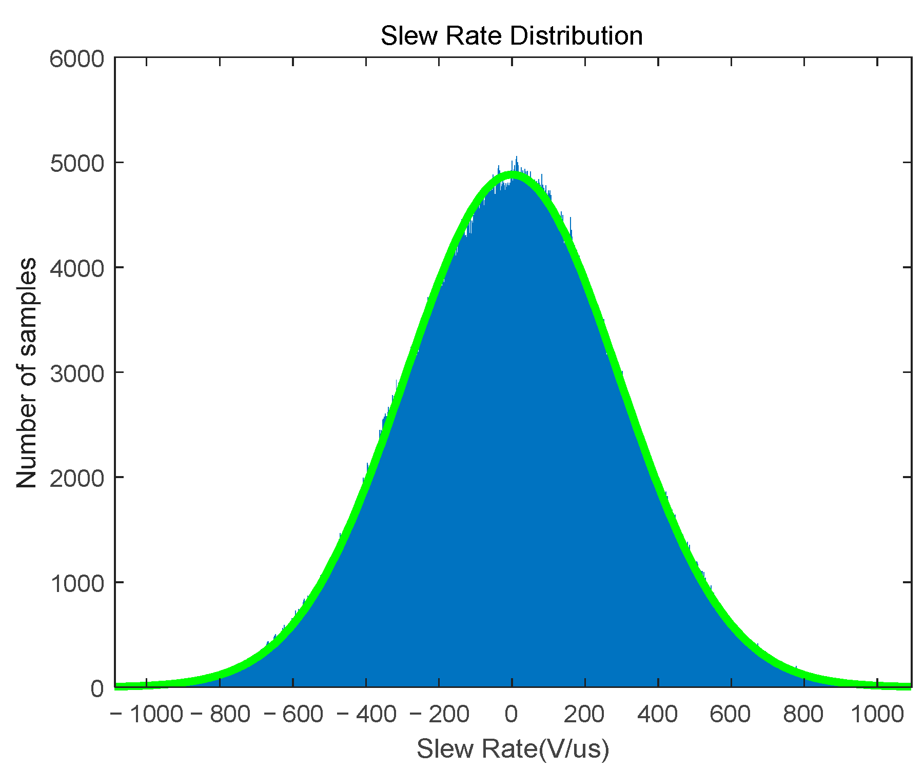
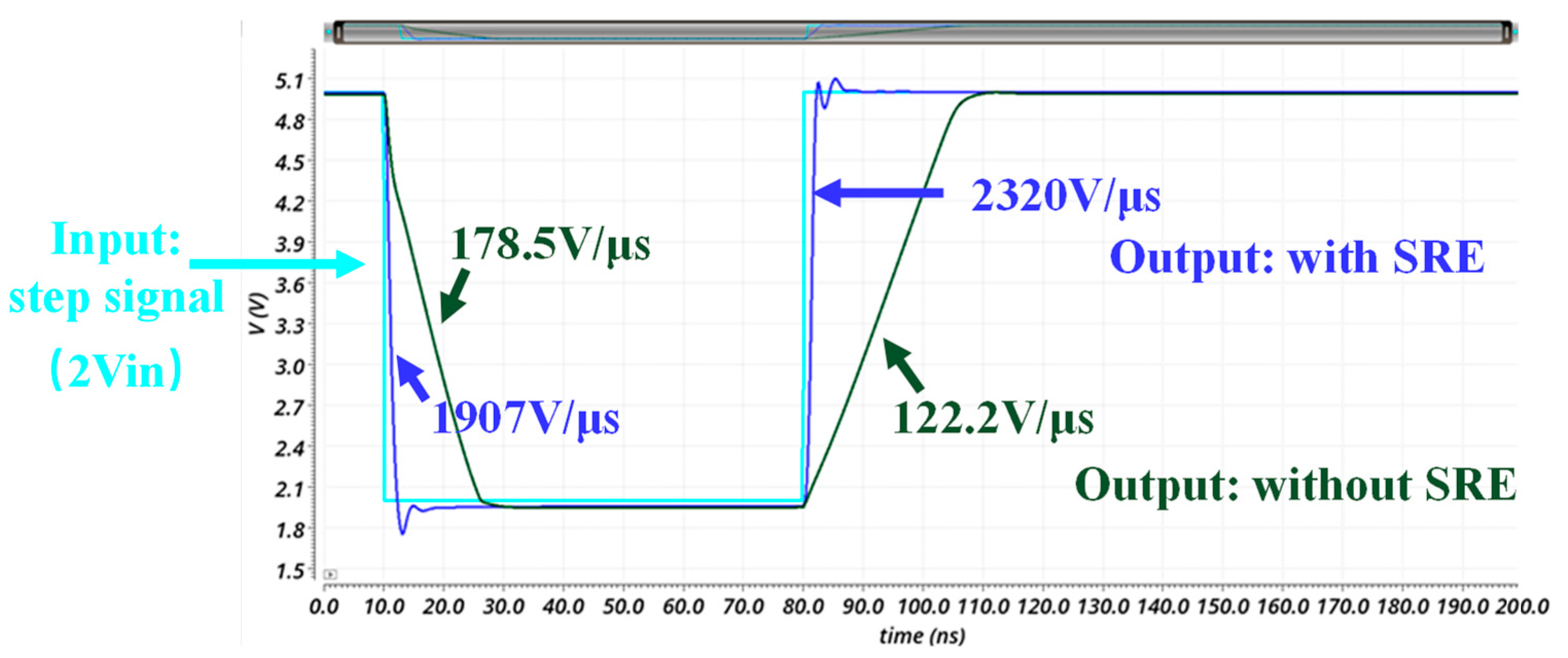
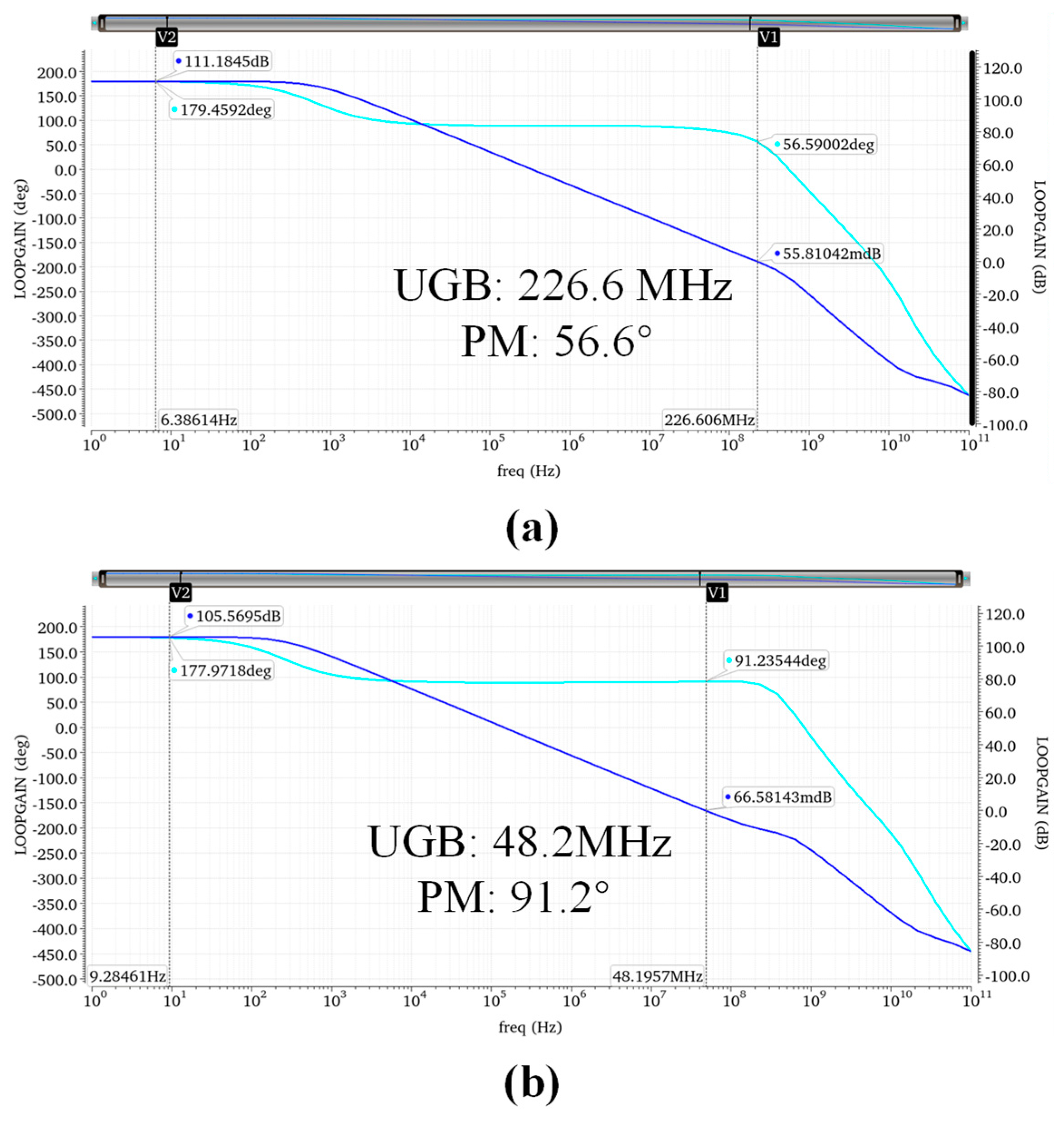
2.2.3. Simulation Results

To better understand the effectiveness of the proposed SRE circuit, we compared the simulated LA performances with and without the SRE circuit. As shown in Figure 12, the proposed SRE structure increased the rise slew rate from 122.2   V / μ s to 2320   V / μ s and the fall slew rate from 178.5   V / μ s to 1907   V / μ s .
As shown in Figure 13, the UGB of the proposed LA was 226.6 MHz, which is four times the one without the SRE circuit.
Table 1 shows more details of the comparison between the proposed LA and the conventional LA. The proposed SRE circuit brought about an increase in the slew rate of over tenfold, while the quiescent current only increased by 50%.
To ensure the robustness of the design, simulations were conducted under different process corners and temperatures. The results are shown in Table 2.
As we can see, the UGB of the LA was greater than 200 MHz in most cases, and based on the phase margin criteria, the stability of the LA was ensured. The quiescent current increased as the temperature rose. In the worst case (slow process corner and 85°C), the slew rate of the LA still reached approximately 1000 V/µs.

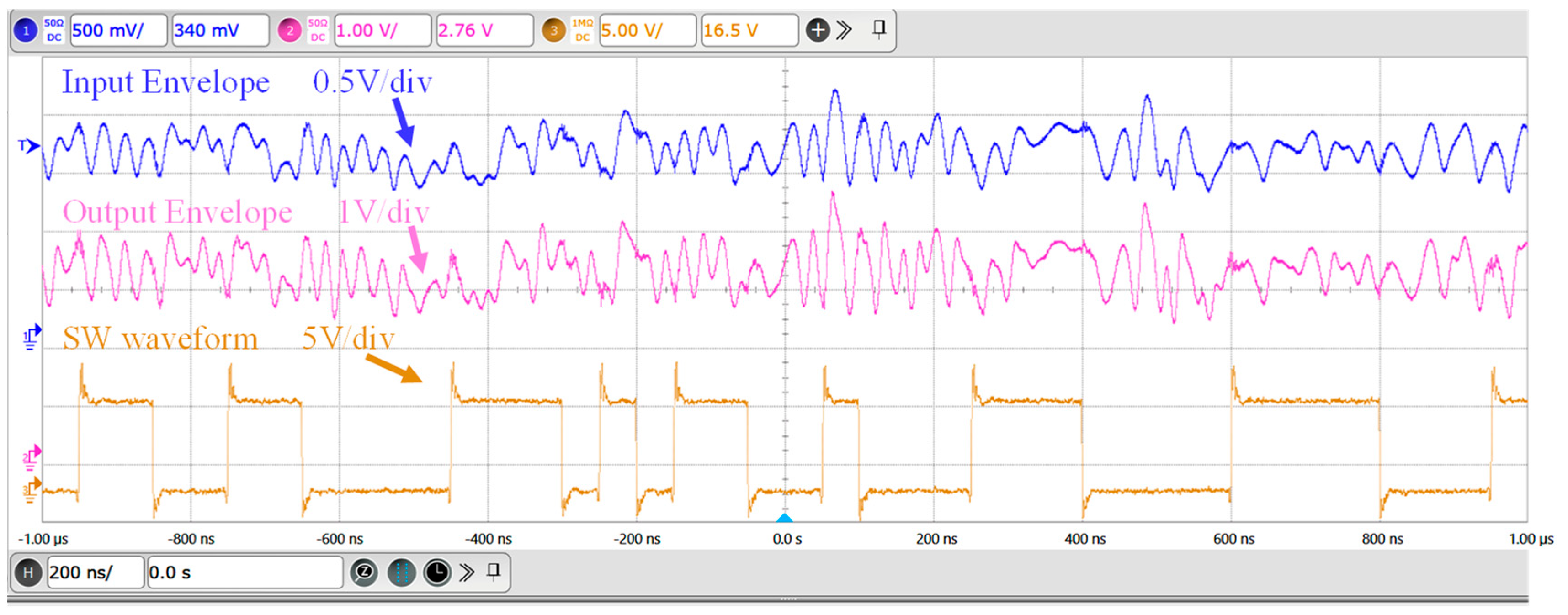
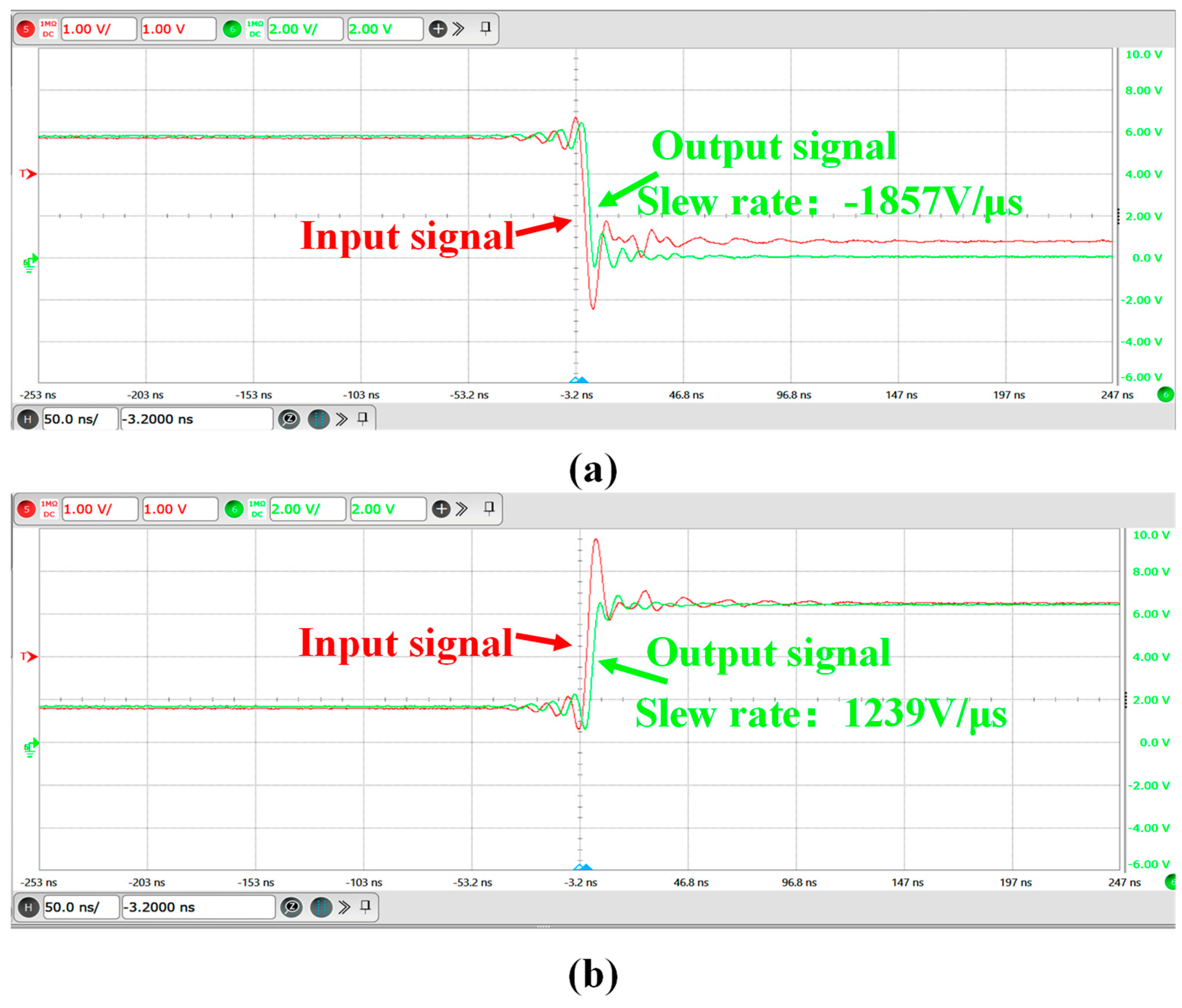
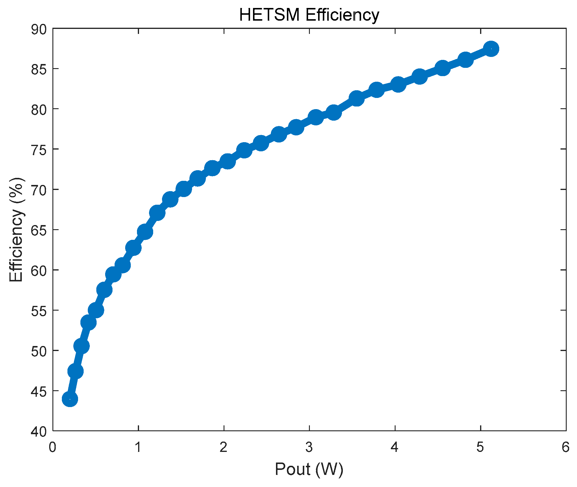
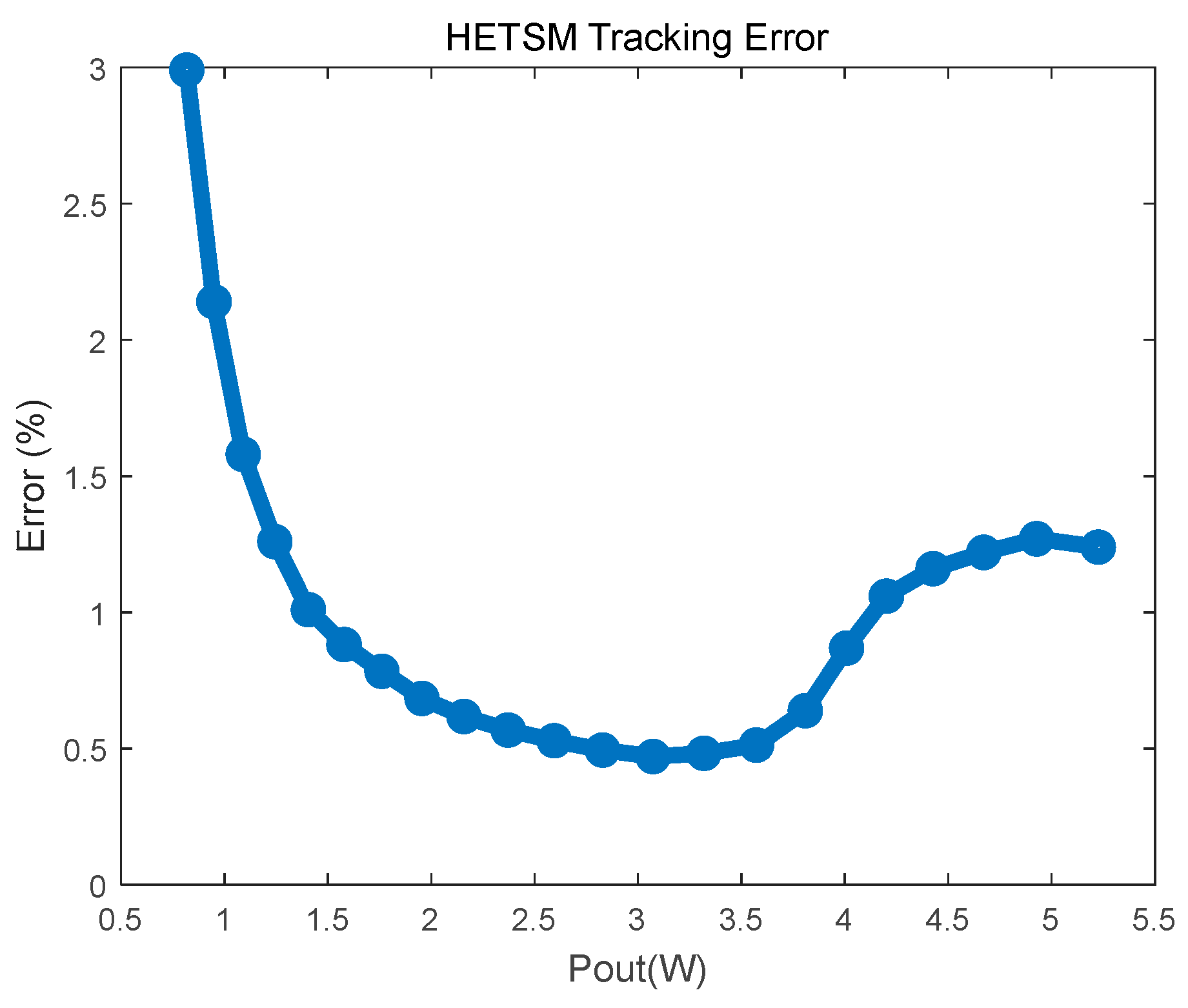
3. Experimental Results

The proposed HETSM chip was fabricated on a 180 nm CMOS process, of which the die size was 1.98 mm × 0.9 mm, as depicted in Figure 14. The chip was operating under a 6.5 V power supply, with an off-chip inductor of 4.7 μ H .
Figure 15 shows the measured waveforms for a 100 MHz signal, with a 16QAM modulation and an 8.49 dB PAPR. The external clock frequency was set to 20 MHz. The input envelope signal, output signal, and switching node voltage are shown in the figure. The HETSM amplified the amplitude of the input signal by a factor of 2, with an output signal delay of 7.5 ns.
Figure 16 illustrates the measured step response waveform of the proposed LA with the SRE circuit. A 100 pF capacitor was connected to the output of LA as a capacitive load. The rise time slew rate was measured at 1239   V / μ s , while the fall time slew rate was measured at 1857   V / μ s .
Figure 17 presents the measured efficiency of the HETSM chip with a 5 Ω load paralleled with a 100 pF capacitor. For the 100 MHz, 16QAM, and 8.49 dB PAPR signal, the peak efficiency reached 87.4%. When the output power was small, the ratio of these intrinsic losses to the output power was relatively large. According to Equation (3), the efficiency was relatively small under low-power conditions for the large value of the aforementioned ratio, as shown in Figure 17.
Figure 18 shows the measured error between the output voltage and the ideal output voltage when tracking the 100 MHz, 16QAM envelope signal. The tracking error was less than 3%.
The comparison of the proposed HETSM with prior works is shown in Table 3. Our work showed the highest slew rate of LA and adapted the 100 MHz wideband signal tracking. Also, it achieved 87.4% efficiency, which is comparable to prior works. The proposed HETSM provided a maximum voltage of 6 V, which can accommodate GaAs PA applications.

4. Conclusions

In this work, we designed an HETSM with a slew-rate-enhanced LA. The proposed SRE structure introduced a parallel auxiliary current path directly to the gate of the output stage, significantly accelerating the charging and discharging processes of the Miller capacitor without modifying the operating point of the remaining LA. Assisted by the quadratically growing SRE current, the proposed LA with the SRE circuit achieved a high slew rate and a large bandwidth under low quiescent current conditions. The presented HETSM chip was fabricated using the 180 nm CMOS process. The proposed LA with the SRE circuit achieved a slew rate of 1239   V / μ s for rising edges and −1857   V / μ s for falling edges at a quiescent current of 24 mA. Therefore, it established a solid foundation for ET modulators to track the wideband envelope signal. The proposed HETSM achieved a maximum efficiency of 87.4% while tracking a 100 MHz, 16QAM, and 8.49 dB PAPR signal.

Supplementary Materials

The following supporting information can be downloaded at: https://www.mdpi.com/article/10.3390/electronics13142701/s1, Document S1: “AC analysis of the linear amplifier (LA) with the proposed SRE circuit”.

Author Contributions

Software, K.Z.; methodology, X.L.; formal analysis, J.W. and H.Z.; validation, H.C. and X.L.; data curation, K.Z., J.W., H.Z. and Z.S.; writing—original draft preparation, K.Z.; writing—review and editing, Z.W.; supervision, F.Y. All authors have read and agreed to the published version of the manuscript.

Funding

This research received no external funding.

Data Availability Statement

Data is contained within the article.

Conflicts of Interest

Authors Jianhui Wu, Huabao Zhuang, Zhening Shi were employed by Zhejiang Hangxinyuan IC Technology Company. The remaining authors declare that the research was conducted in the absence of any commercial or financial relationships that could be construed as a potential conflict of interest.

References

  1. Wang, Z. Envelope Tracking Power Amplifiers for Wireless Communications; Artech House: Boston, MA, USA, 2014; pp. 4–7. ISBN 978-1-60807-784-7. [Google Scholar]
  2. Ruan, X.; Wang, Y.; Jin, Q. A Review of Envelope Tracking Power Supply for Mobile Communication Systems. CPSS Trans. Power Electron. Appl. 2017, 2, 277–291. [Google Scholar] [CrossRef]
  3. Asbeck, P.; Popovic, Z. ET Comes of Age: Envelope Tracking for Higher-Efficiency Power Amplifiers. IEEE Microw. Mag. 2016, 17, 16–25. [Google Scholar] [CrossRef]
  4. Watkins, G.T.; Mimis, K. How Not to Rely on Moore’s Law Alone: Low-Complexity Envelope-Tracking Amplifiers. IEEE Microw. Mag. 2018, 19, 84–94. [Google Scholar] [CrossRef]
  5. Paek, J.-S.; Kim, D.; Choo, Y.; Youn, Y.-S.; Lee, J.; Cho, T.B.-H. Design of Boosted Supply Modulator With Reverse Current Protection for Wide Battery Range in Envelope Tracking Operation. IEEE Trans. Microw. Theory Tech. 2019, 67, 183–194. [Google Scholar] [CrossRef]
  6. Leng, Y.; Ruan, X.; Jin, Q.; Wang, Y. High-Efficiency High-Bandwidth Switch-Linear Hybrid Envelope-Tracking Power Supply with Slew Rate Split-Band Method. In Proceedings of the 2017 IEEE Energy Conversion Congress and Exposition (ECCE), Cincinnati, OH, USA, 1–5 October 2017; pp. 2246–2252. [Google Scholar] [CrossRef]
  7. Komatsuzaki, Y.; Lanfranco, S.; Kolmonen, T.; Piirainen, O.; Tanskanen, J.K.; Sakata, S.; Ma, R.; Shinjo, S.; Yamanaka, K.; Asbeck, P. A High Efficiency 3.6–4.0 GHz Envelope-Tracking Power Amplifier Using GaN Soft-Switching Buck-Converter. In Proceedings of the 2018 IEEE/MTT-S International Microwave Symposium—IMS, Philadelphia, PA, USA, 10–15 June 2018; pp. 465–468. [Google Scholar] [CrossRef]
  8. He, H.; Ge, T.; Chang, J. A Review on Supply Modulators for Envelope-Tracking Power Amplifiers. In Proceedings of the 2016 International Symposium on Integrated Circuits (ISIC), Singapore, 12–14 December 2016; pp. 1–4. [Google Scholar] [CrossRef]
  9. Mahmoudidaryan, P.; Mandal, D.; Bakkaloglu, B.; Kiaei, S. Wideband Hybrid Envelope Tracking Modulator With Hysteretic-Controlled Three-Level Switching Converter and Slew-Rate Enhanced Linear Amplifier. IEEE J. Solid-State Circuits 2019, 54, 3336–3347. [Google Scholar] [CrossRef]
  10. Chen, Z.; Xia, Q.; Dong, L.; Fan, S.; Han, K.; Guo, Z.; Xue, Z.; Geng, L. An Open Loop Digitally Controlled Hybrid Supply Modulator Achieving High Efficiency for Envelope Tracking With Baseband up to 200-MHz. IEEE Trans. Circuits Syst. I Regul. Pap. 2020, 67, 4142–4153. [Google Scholar] [CrossRef]
  11. Hsu, Y.-T.; Lin, Z.-Y.; Lee, J.-J.; Chen, K.-H. An Envelope Tracking Supply Modulator Utilizing a GaN-Based Integrated Four-Phase Switching Converter and Average Power Tracking-Based Switch Sizing With 85.7% Efficiency for 5G NR Power Amplifier. IEEE J. Solid-State Circuits 2021, 56, 3167–3176. [Google Scholar] [CrossRef]
  12. Chen, D.; Zhao, C.; Xiong, Y.; Wu, Y.; Ban, Y.; Liu, Y.; Liu, H.; Kang, K. An Asynchronous Dual Switch Envelope Tracking Supply Modulator with 86% Efficiency. IEICE Electron. Express 2018, 15, 20180206. [Google Scholar] [CrossRef]
  13. Kwak, M.; Jeong, J.; Hassan, M.; Yan, J.J.; Kimball, D.F.; Asbeck, P.M.; Larson, L.E. High Efficiency Wideband Envelope Tracking Power Amplifier with Direct Current Sensing for LTE Applications. In Proceedings of the 2012 IEEE Topical Conference on Power Amplifiers for Wireless and Radio Applications, Santa Clara, CA, USA, 15–18 January 2012; pp. 41–44. [Google Scholar] [CrossRef]
  14. He, H.; Ge, T.; Kang, Y.; Guo, L.; Chang, J.S. A 40 MHz Bandwidth, 91% Peak Efficiency, 2.5 W Output Power Supply Modulator With Dual-Mode Sigma–Delta Control and Adaptive Biasing Amplifier for Multistandard Communications. IEEE Trans. Power Electron. 2020, 35, 9430–9442. [Google Scholar] [CrossRef]
  15. Leng, Y.; Ruan, X.; Jin, Q.; Wang, Y. Current Control Strategies for Parallel-Form Switch-Linear Hybrid Envelope Tracking Power Supply With Two Switched-Mode Converters to Achieve Optimal Power Allocation. IEEE J. Emerg. Sel. Top. Power Electron. 2019, 7, 2356–2368. [Google Scholar] [CrossRef]
  16. Choi, J.; Kim, D.; Kang, D.; Kim, B. A New Power Management IC Architecture for Envelope Tracking Power Amplifier. IEEE Trans. Microw. Theory Tech. 2011, 59, 1796–1802. [Google Scholar] [CrossRef]
  17. Cao, T.; Huang, F.; Zhang, Q.; Liu, Y. High Efficiency and Wideband Hybrid Envelope Amplifier for Envelope Tracking Operation of Wireless Transmitter. In Proceedings of the 2018 IEEE MTT-S International Wireless Symposium (IWS), Chengdu, China, 6–10 May 2018; pp. 1–4. [Google Scholar] [CrossRef]
  18. Xu, P.; Zhang, X.; Cao, P.; Wei, T.; Tong, Z.; Zeng, X.; Xu, J.; Hong, Z. A 2.7 W AC-Coupled Hybrid Supply Modulator Achieving 200 MHz Envelope-Tracking Bandwidth for 5G New Radio Power Amplifier. IEEE Trans. Power Electron. 2023, 38, 7416–7427. [Google Scholar] [CrossRef]
  19. Leng, W.; Abidi, A.A.; Mundlapudi, S.R.; Darabi, H.; Chowdhury, D.; Afsahi, A.; Li, S. Envelope Tracking Supply Modulator with Trellis-Search-Based Switching and 160-MHz Capability. IEEE J. Solid-State Circuits 2022, 57, 719–733. [Google Scholar] [CrossRef]
  20. Jing, Y.; Bakkaloglu, B. A High Slew-Rate Adaptive Biasing Hybrid Envelope Tracking Supply Modulator for LTE Applications. IEEE Trans. Microw. Theory Tech. 2017, 65, 3245–3256. [Google Scholar] [CrossRef]
  21. Li, S.; Yu, K.; Ou, L.; Zhou, P.; Zhang, G. A Compact Hybrid Envelope Tracking Supply Modulator with Wide-Band High-Slew-Rate Linear Amplifier. IEICE Electron. Express 2020, 17, 20200121. [Google Scholar] [CrossRef]
  22. Li, W.; Bartzoudis, N.; Rubio Fernández, J.; López-Bueno, D.; Montoro, G.; Gilabert, P.L. FPGA Implementation of a Linearization System for Wideband Envelope Tracking Power Amplifiers. IEEE Trans. Microw. Theory Tech. 2023, 71, 1781–1792. [Google Scholar] [CrossRef]
  23. Montoro, G.; Gilabert, P.L.; Vizarreta, P.; Bertran, E. Slew-Rate Limited Envelopes for Driving Envelope Tracking Amplifiers. In Proceedings of the 2011 IEEE Topical Conference on Power Amplifiers for Wireless and Radio Applications, Phoenix, AZ, USA, 16–19 January 2011; pp. 17–20. [Google Scholar] [CrossRef]
  24. Yen, A.; Blalock, B.J. A High Slew Rate, Low Power, Compact Operational Amplifier Based on the Super-Class AB Recycling Folded Cascode. In Proceedings of the 2020 IEEE 63rd International Midwest Symposium on Circuits and Systems (MWSCAS), Springfield, MA, USA, 9–12 August 2020; pp. 9–12. [Google Scholar] [CrossRef]
  25. Kwong, K.Y.; Leung, K.N. Slew-Rate Enhancement Circuit of CMOS Current-Mirror Amplifier by Edge-Detecting Technique. In Proceedings of the 2010 IEEE International Conference of Electron Devices and Solid-State Circuits (EDSSC), Hong Kong, China, 15–17 December 2010; pp. 1–4. [Google Scholar] [CrossRef]
  26. Panda, B.; Dash, S.K.; Mishra, S.N. High Slew Rate Op-Amp Design for Low Power Applications. In Proceedings of the 2014 International Conference on Control, Instrumentation, Communication and Computational Technologies (ICCICCT), Kanyakumari, India, 10–11 July 2014; pp. 1096–1100. [Google Scholar] [CrossRef]
  27. Li, P.; Wei, Q.; Luo, L. Slew-Rate Enhancement Circuit of CLASS AB Operational Transconductance Amplifier (OTA) by Auxiliary Circuit. In Proceedings of the 2022 IEEE 4th International Conference on Circuits and Systems (ICCS), Chengdu, China, 23–26 September 2022; pp. 1–5. [Google Scholar] [CrossRef]
  28. Zhang, M.; Wang, X.; Liu, H.; Qi, X.; Li, X.; Wang, S. Class-AB Operational Amplifier with Current Domain Slew-Rate Enhancement. In Proceedings of the 2022 IEEE 5th International Conference on Electronics Technology (ICET), Chengdu, China, 13–16 May 2022; pp. 142–146. [Google Scholar] [CrossRef]
Figure 1. Power dissipation comparison between the ET PA and the traditional PA.
Electronics 13 02701 g001
Figure 2. The proposed HETSM diagram.
Electronics 13 02701 g002
Figure 3. Slew-rate distribution of a 100 MHz, 16QAM envelope signal.
Electronics 13 02701 g003
Figure 4. Diagram of the proposed LA design with an SRE structure.
Electronics 13 02701 g004
Figure 5. (a) The entire LA circuit. (b) The proposed SRE circuit.
Electronics 13 02701 g005
Figure 6. SRE current vs. the input voltage: (a) primary: I S R 1 and I S R 2 . (b) Output: I S R P and I S R N .
Electronics 13 02701 g006
Figure 7. Transition state: (a) V I N P < V I N N and (b) V I N P > V I N N .
Electronics 13 02701 g007
Figure 8. A small-signal model of the SRE circuit.
Electronics 13 02701 g008
Figure 9. A small-signal model of the proposed LA’s input stage.
Electronics 13 02701 g009
Figure 10. The small-signal model of the entire LA.
Electronics 13 02701 g010
Figure 11. The simplified model of the entire LA.
Electronics 13 02701 g011
Figure 12. The simulated step response of the LA with the proposed SRE structure.
Electronics 13 02701 g012
Figure 13. Loop gain of the LA (a) with the proposed SRE structure and (b) without SRE.
Electronics 13 02701 g013
Figure 14. The micrograph of the proposed HETSM.
Electronics 13 02701 g014
Figure 15. The measured transient response of the ET modulator to the 100 MHz envelope signal.
Electronics 13 02701 g015
Figure 16. Measured step responses of the proposed LA with the SRE circuit: (a) fall condition and (b) rise condition.
Electronics 13 02701 g016
Figure 17. Measured efficiency of the HETSM chip with the 100 MHz envelope signal.
Electronics 13 02701 g017
Figure 18. Measured tracking error between the output and the ideal output voltage with the 100 MHz envelope signal.
Electronics 13 02701 g018
Table 1. Simulation results of the proposed LA and the conventional LA.
DesignConventional LA
(Without SRE)
The Proposed LA
(With SRE)
UGB (MHz)48.2226.6
Phase Margin (°)91.256.6
DC Gain (dB)105.6111.2
Slew   Rate   ( V / μ s )−178.5/+122.2−1907/+2320
Quiescent Current (mA)16.224
Table 2. Performance of LA under different process corners and temperature conditions.
ProcessTemperature (°C)DC Gain (dB)Phase Margin (°)UGB (MHz)Quiescent Current (mA)Positive Slew Rate (V/us)Negative Slew Rate (V/us)
ff lib−4011762209.720.14311−3246
25108.861.3216.926.23513−3738
8596.960.7213.332.31908−1920
tt lib−40118.365.3212.619.53268−2454
25111.458.9228.626.02583−1926
85101.854.3227.432.32034−1378
ss lib−40116.662.4200.521.32222−1775
25108.554.120229.51747−1345
8593.867.9153.537.41325−983
Table 3. Performance comparison with prior works.
DesignProcess (nm)Signal Bandwidth(MHz)PAPR (dB)Die Area
(mm2)
LA ArchitectureMax ET Voltage (V)Load
Conditions
Slew   Rate   of   LA   ( V / μ s )Max Tracking Error I Q of LA (mA)Max Efficiency of ET System
JSSC2019 [9]65LTE 40/807.84@40 MHz
8.06@80 MHz
total: 2 × 2 = 4
core: 1.6 × 2.4 = 2.72
parallel current–mirror SRE path2.44.7 Ω−307/+3252.3%@40 MHz
3.2%@80 MHz
NA93%@40 MHz
91%@80 MHz
MTT2017 [20]180LTE 107.24core: 1.05 × 1.05 = 1.1adaptive biasing using the FVF structure3.46 Ω||150 pF−152.5/+93.4NA1483%
IEICE2020 [21]180LTE 106total: 1.55 × 0.8 = 1.24 core: 0.78enhanced current–mirror structure35–20 Ω−160/+2201.5%1283%
this work180100 (16QAM)8.49total: 1.98 × 0.9 = 1.79 core: 1.55 × 0.6 = 0.93parallel nonlinear current–SRE path65 Ω||100 pF−1857/+12393%2487.4%
Disclaimer/Publisher’s Note: The statements, opinions and data contained in all publications are solely those of the individual author(s) and contributor(s) and not of MDPI and/or the editor(s). MDPI and/or the editor(s) disclaim responsibility for any injury to people or property resulting from any ideas, methods, instructions or products referred to in the content.

