
Compact, Ultra-Wideband Butler Matrix Beamformers for the Advanced 5G Band FR3—Part I

 ,
,  , ,
, ,  and
and 
Abstract
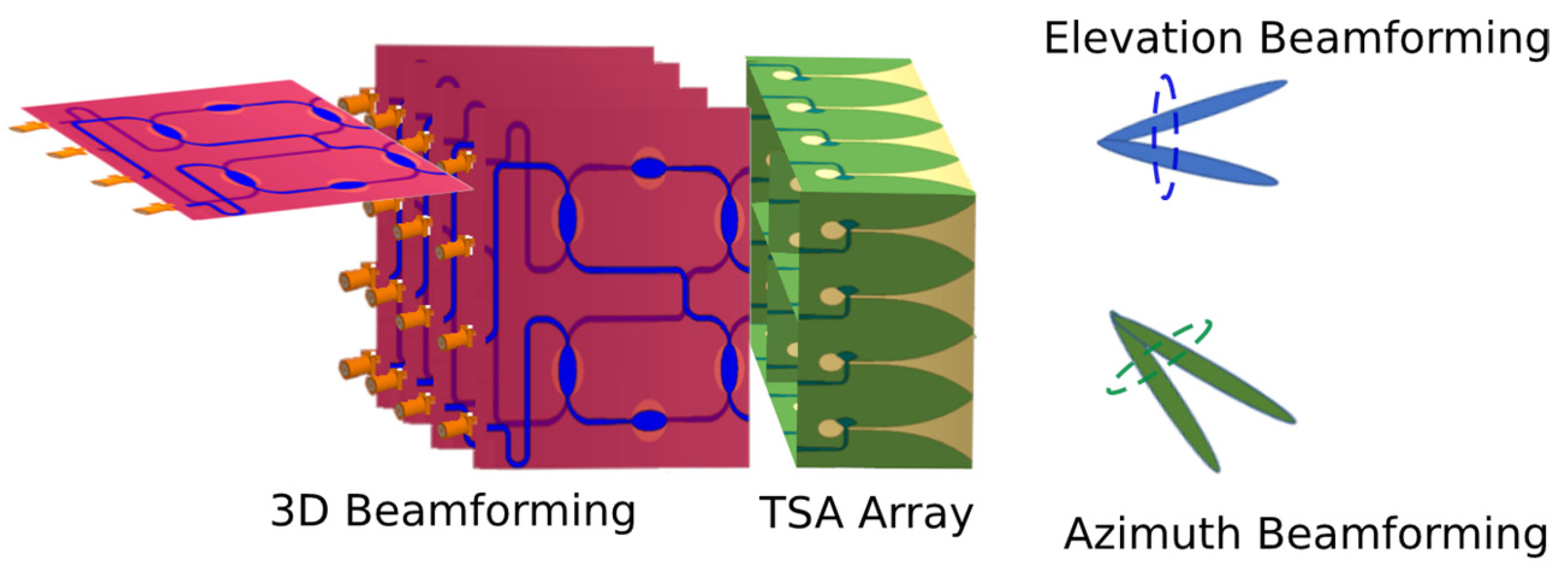
:1. Introduction—FR3 Use for eMMB via Analog Beamformers
2. Butler Matrix Design
2.1. Butler-Matrix Components’ Design
2.1.1. The 3 dB/90° Hybrid Coupler
2.1.2. Phase Shifter and Meander Lines
2.1.3. Equiphased Transmission Line Network
2.2. BM Design Employing Wideband-Matching Technique
3. Butler Matrix Results
3.1. First Design Approach’s 8 × 8 BM Results
3.2. BM Results of the 2nd Design Approach
4. Conclusions
Author Contributions
Funding
Data Availability Statement
Conflicts of Interest
References
- He, L.-H.; Ban, Y.-L.; Yan, F.-Q.; Wu, G. Dual-Polarized Two-Dimensional Multibeam Antenna Array With Hybrid Beamforming and Its Planarization. IEEE Access 2021, 9, 54951–54961. [Google Scholar] [CrossRef]
- Payami, S.; Khalily, M.; Araghi, A.; Loh, T.H.; Cheadle, D.; Nikitopoulos, K.; Tafazolli, R. Developing the First mmWave Fully-Connected Hybrid Beamformer With a Large Antenna Array. IEEE Access 2020, 8, 41282–141291. [Google Scholar] [CrossRef]
- Hu, Y.; Zhan, J.; Jiang, Z.H.; Yu, C.; Hong, W. An Orthogonal Hybrid Analog–Digital Multibeam Antenna Array for Millimeter-Wave Massive MIMO Systems. IEEE Trans. Antennas Propag. 2021, 69, 1393–1403. [Google Scholar] [CrossRef]
- Larsson, E.G.; Edfors, O.; Tufvesson, F.; Marzetta, T.L. Massive MIMO for next Generation Wireless Systems. IEEE Commun. Mag. 2014, 52, 186–195. [Google Scholar] [CrossRef]
- Babur, G.; Manokhin, G.O.; Geltser, A.A.; Shibelgut, A.A. Low-Cost Digital Beamforming on Receive in Phased Array Radar. IEEE Trans. Aerosp. Electron. Syst. 2017, 53, 1355–1364. [Google Scholar] [CrossRef]
- Venkateswaran, V.; van der Veen, A.-J. Analog Beamforming in MIMO Communications With Phase Shift Networks and Online Channel Estimation. IEEE Trans. Signal Process 2010, 58, 4131–4143. [Google Scholar] [CrossRef]
- Ahmed, I.; Khammari, H.; Shahid, A.; Musa, A.; Kim, K.S.; De Poorter, E.; Moerman, I. A Survey on Hybrid Beamforming Techniques in 5G: Architecture and System Model Perspectives. IEEE Commun. Surv. Tutor. 2018, 20, 3060–3097. [Google Scholar] [CrossRef]
- Shallah, A.B.; Zubir, F.; Rahim, M.K.A.; Majid, H.A.; Ullah Sheikh, U.; Murad, N.A.; Yusoff, Z. Recent Developments of Butler Matrix From Components Design Evolution to System Integration for 5G Beamforming Applications: A Survey. IEEE Access 2022, 10, 88434–88456. [Google Scholar] [CrossRef]
- Lialios, D.I.; Ntetsikas, N.; Paschaloudis, K.D.; Zekios, C.L.; Georgakopoulos, S.V.; Kyriacou, G.A. Design of True Time Delay Millimeter Wave Beamformers for 5G Multibeam Phased Arrays. Electronics 2020, 9, 1331. [Google Scholar] [CrossRef]
- Fonseca, N.J.G. Printed S-Band 4 × 4 Nolen Matrix for Multiple Beam Antenna Applications. IEEE Trans. Antennas Propag. 2009, 57, 1673–1678. [Google Scholar] [CrossRef]
- Butler, J. Beam-Forming Matrix Simplifies Design of Electronically Scanned Antennas. Electron. Des. 1961, 9, 170–173. [Google Scholar]
- Vallappil, A.K.; Rahim, M.K.A.; Khawaja, B.A.; Murad, N.A.; Mustapha, M.G. Butler Matrix Based Beamforming Networks for Phased Array Antenna Systems: A Comprehensive Review and Future Directions for 5G Applications. IEEE Access 2021, 9, 3970–3987. [Google Scholar] [CrossRef]
- Wang, C.-W.; Ma, T.-G.; Yang, C.-F. A New Planar Artificial Transmission Line and Its Applications to a Miniaturized Butler Matrix. IEEE Trans. Microw. Theory Technol. 2007, 55, 2792–2801. [Google Scholar] [CrossRef]
- Jeong, Y.S.; Kim, T.W. Design and Analysis of Swapped Port Coupler and Its Application in a Miniaturized Butler Matrix. IEEE Trans. Microw. Theory Technol. 2010, 58, 764–770. [Google Scholar] [CrossRef]
- Tian, G.; Yang, J.-P.; Wu, W. A Novel Compact Butler Matrix Without Phase Shifter. IEEE Microw. Wirel. Compon. Lett. 2014, 24, 306–308. [Google Scholar] [CrossRef]
- Wen, J.M.; Wang, C.K.; Hong, W.; Pan, Y.M.; Zheng, S.Y. A Wideband Switched-Beam Antenna Array Fed by Compact Single-Layer Butler Matrix. IEEE Trans. Antennas Propag. 2021, 69, 5130–5135. [Google Scholar] [CrossRef]
- Bembarka, A.; Setti, L.; Tribak, A.; Tizyi, H.; El Ouahabi, M. A Novel Wideband Beamforming Antenna for 5G Applications by Eliminating the Phase Shifters and Crossovers from the Butler Matrix. Prog. Electromagn. Res. C 2023, 133, 51–63. [Google Scholar] [CrossRef]
- Sakhiya, R.; Chowdhury, S. A Low-Loss, 77 GHz, 8 × 8 Microstrip Butler Matrix on a High-Purity Fused-Silica (HPFS) Glass Substrate. Sensors 2023, 23, 1418. [Google Scholar] [CrossRef]
- Tajik, A.; Shafiei Alavijeh, A.; Fakharzadeh, M. Asymmetrical 4 × 4 Butler Matrix and Its Application for Single Layer 8 × 8 Butler Matrix. IEEE Trans. Antennas Propag. 2019, 67, 5372–5379. [Google Scholar] [CrossRef]
- Shady, M.O.; Kishk, A.A. Compact 4 × 4 Multilayer Butler Matrix With Four-Slot Array. IEEE Trans. Microw. Theory Technol. 2024, 72, 3522–3529. [Google Scholar] [CrossRef]
- Jung, J.; Ryu, J.; Jung, K.-Y. Multi-Beam 5G Antenna With Miniaturized Butler Matrix Using Stacked LTCC. IEEE Access 2023, 11, 125519–125528. [Google Scholar] [CrossRef]
- Van Messem, L.; Moerman, A.; Caytan, O.; de Paula, I.L.; Hoflack, B.; Stroobandt, B.; Lemey, S.; Moeneclaey, M.; Rogier, H. A 4 × 4 Millimeter wave-Frequency Butler Matrix in Grounded Co-Planar Waveguide Technology for Compact Integration With 5G Antenna Arrays. IEEE Trans. Microw. Theory Technol. 2023, 71, 122–134. [Google Scholar] [CrossRef]
- Lin, T.-H.; Hsu, S.-K.; Wu, T.-L. Bandwidth Enhancement of 4 × 4 Butler Matrix Using Broadband Forward-Wave Directional Coupler and Phase Difference Compensation. IEEE Trans. Microw. Theory Technol. 2013, 61, 4099–4109. [Google Scholar] [CrossRef]
- Ausordin, S.F.; Abdul Rahim, S.K.; Seman, N.; Dewan, R.; Sa’ad, B. A Compact 4 × 4 Butler Matrix on Double-Layer Substrate. Microw. Opt. Technol. Lett. 2014, 56, 223–229. [Google Scholar] [CrossRef]
- Fanyaev, I.; Faniayeu, I. Synthesis of Novel 8 × 8 Beam-Forming Network for Broadband Multibeam Antenna Array. Int. J. RF Microw. Comput.-Aided Eng. 2022, 32, e22970. [Google Scholar] [CrossRef]
- Zhai, Y.; Fang, X.; Ding, K.; He, F. Miniaturization Design for 8 × 8 Butler Matrix Based on Back-to-Back Bilayer Microstrip. Int. J. Antennas Propag. 2014, 2014, 583903. [Google Scholar] [CrossRef]
- Shao, Q.; Chen, F.-C.; Wang, Y.; Chu, Q.-X. Design of 4 × 4 and 8 × 8 Filtering Butler Matrices Utilizing Combined 90° and 180° Couplers. IEEE Trans. Microw. Theory Technol. 2021, 69, 3842–3852. [Google Scholar] [CrossRef]
- Wincza, K.; Gruszczynski, S. Broadband Integrated 8 × 8 Butler Matrix Utilizing Quadrature Couplers and Schiffman Phase Shifters for Multibeam Antennas With Broadside Beam. IEEE Trans. Microw. Theory Technol. 2016, 64, 2596–2604. [Google Scholar] [CrossRef]
- Wincza, K.; Gruszczynski, S.; Sachse, K. Broadband Planar Fully Integrated 8 × 8 Butler Matrix Using Coupled-Line Directional Couplers. IEEE Trans. Microw. Theory Technol. 2011, 59, 2441–2446. [Google Scholar] [CrossRef]
- Bantavis, P.I.; Kolitsidas, C.I.; Empliouk, T.; Le Roy, M.; Jonsson, B.L.G.; Kyriacou, G.A. A Cost-Effective Wideband Switched Beam Antenna System for a Small Cell Base Station. IEEE Trans. Antennas Propag. 2018, 66, 6851–6861. [Google Scholar] [CrossRef]
- Fakoukakis, F.E.; Kaifas, T.N.; Vafiadis, E.E.; Kyriacou, G.A. Design and Implementation of Butler Matrix-Based Beam-Forming Networks for Low Sidelobe Level Electronically Scanned Arrays. Int. J. Microw. Wirel. Technol. 2015, 7, 69–79. [Google Scholar] [CrossRef]
- Empliouk, T.M.; Bantavis, P.I.; Koltsidas, C.I.; Kaifas, T.N.F.; Kyriacou, G.A. Ultra-Wideband Six-Port Network Miniaturization—Matching. Int. J. Microw. Wirel. Technol. 2023, 15, 1676–1688. [Google Scholar] [CrossRef]
- Balanis, C.A. Antenna Theory: Analysis and Design, 2nd ed.; John Wiley & Sons, Inc.: New York, NY, USA, 1997. [Google Scholar]
- Pozar, D.M. Microwave Engineering, 3rd ed.; Wiley: New York, NY, USA, 2011. [Google Scholar]


| Reference | Technology | OB (GHz) | f0 (GHz) | FBW (%) | Size (mm2) | NS (λ) | FA (λ2) | ILAv ± ΔA (dB) | PA (°) |
|---|---|---|---|---|---|---|---|---|---|
| [20] | Microstrip to Slot | 27–31 | 29 | 13.8 | 3.49 × 2.2 | 7.67 | −9 ± 1.4 | ±8 | |
| [21] | LTCC | 26–30 | 28 | 14 | 22.02 × 5.93 | 2.05 × 0.55 | 1.12 | −9 ± 3.5 | ±9 |
| [22] | GCPW | 23.75–31 | 27 | 26.5 | 19.2 × 29.84 | 1.8 × 2.8 | 5.04 | −9 ± 4 | - |
| [23] | FWDC | 1.9–3.1 | 2.5 | 47 | 81.65 × 71.56 | 0.68 × 0.59 | 0.4 | −7 ± 3 | ±6 |
| [24] | Microstrip to Slot | 2–3 | 2.45 | 40 | 100 × 120 | 0.8 × 0.98 | 0.78 | −7 ± 3 | ±7 |
| This Work | Microstrip to Slot | 6–16 | 9.8 | 102 | 39.4 × 17.9 | 1.28 × 0.58 | 0.74 | −7 ± 2 | ±9 |
| Reference | Technology | OB (GHz) | f0 (GHz) | FBW (%) | Size (mm2) | NS (λ) | FA (λ2) | ILAv ± ΔA (dB) | PA (°) |
|---|---|---|---|---|---|---|---|---|---|
| [25] | Slotline Transition—Magit T | 7–13 | 10 | 85 | 140 × 97 | 4.7 × 3.2 | 15.04 | −12 ± 2.5 | ±20 |
| [26] | Microstrip | 3.6–4.7 | 4.2 | 26 | 160 × 160 | 2.1 × 2.1 | 4.4 | −12 ± 3 | ±15 |
| [27] | Stripline | 2.3–2.5 | 2.4 | 5.5 | 250 × 160 | 2 × 1.28 | 2.56 | −12 ± 1.9 | ±12 |
| [28] | Stripline | 3 | 33 | 170 × 145 | 1.7 × 1.45 | 2.46 | ±0.5 | ±10 | |
| [29] | Stripline | 2.5–3.5 | 3 | 33 | 130 × 100 | 1.3 × 1 | 1.3 | ±0.45 | ±7.5 |
| This Work | Microstrip to Slot | 6–16 | 9.8 | 92 | 58.46 × 90 (39.9 × 53.52) | 1.91 × 2.94 (1.3 × 1.74) | 5.6 (2.26) | −12 ± 3 | ±21.5 |
| This Work | Microstrip to Slot | 6–16 | 9.8 | 92 | 40.1 × 84.26 (29.55 × 53.6) | 1.3 × 2.75 (0.96 × 1.75) | 3.57 (1.68) | −12 ± 3 | ±21 |
| Antenna Ports | Beam Ports | |||||||
|---|---|---|---|---|---|---|---|---|
| 1L | 4R | 3L | 2R | 2L | 3R | 4L | 1R | |
| 1 | 90 | −180 | 157.5 | −112.5 | 135 | −135 | 157.5 | −112.5 |
| 2 | 112.5 | 22.5 | −90 | −180 | −157.5 | 112.5 | −45 | −135 |
| 3 | 135 | −135 | 22.5 | 112.5 | 90 | 0 | 112.5 | −157.5 |
| 4 | 157.5 | 67.5 | 135 | 45 | −22.5 | −112.5 | −90 | −180 |
| 5 | −180 | −90 | −112.5 | −22.5 | 45 | 135 | 67.5 | 157.5 |
| 6 | −157.5 | 112.5 | 0 | −90 | 112.5 | 22.5 | −135 | 135 |
| 7 | −135 | −45 | 112.5 | −157.5 | −180 | −90 | 22.5 | 112.5 |
| 8 | −112.5 | 157.5 | −135 | 135 | −112.5 | 157.5 | −180 | 90 |
| Δφ | 22.5 | −157.5 | 112.5 | −67.5 | 67.5 | −112.5 | 157.5 | −22.5 |
| Beam angle | −6° | 46° | −31° | 18° | −18° | 31° | −46° | 6° |
| HC | Cl | Cw | Cs |
|---|---|---|---|
| Theoretical value | 4.57 | 2.29 | 3.44 |
| Simulated value | 4.97 | 2.35 | 3.6 |
| Cw | Cs | Cl | W | l1 | l2 | l3 | lh | lv | r | r1 | ||||
|---|---|---|---|---|---|---|---|---|---|---|---|---|---|---|
| T | S | T | S | T | S | |||||||||
| 22.5° | 4.21 | 3.72 | 5.21 | 5.32 | 5.01 | 4.5 | 0.54 | 1 | 3 | 0.807 | 1.372 | 1.705 | 0.06 | 0.5 |
| 45° | 3.4 | 2.7 | 3.9 | 3.7 | 4.7 | 4.2 | 0.54 | 1 | 7.024 | 0.643 | 1.953 | 4.63 | 0.06 | 0.5 |
| 67.5° | 2.5 | 1.47 | 2.75 | 2.76 | 4.59 | 4.5 | 0.54 | 1 | 3 | 0.807 | 1.372 | 1.801 | 0.06 | 0.5 |
| L1 | L2 | L3 | L4 | w | r | |
|---|---|---|---|---|---|---|
| Line1 | 2 | 0.92 | 14.34 | 8 | 0.54 | 0.5 |
| Line2 | 4 | 0.6 | 15 | 6 | 0.54 | 0.5 |
| Line3 | 6 | 0.469 | 15.2 | 4 | 0.54 | 0.5 |
| Line4 | 8 | 0.06 | 16 | 2 | 0.54 | 0.5 |
| Section | Zlow (Ω) | Zhigh (Ω) | Zm (Ω) | Matching TL | ||||
|---|---|---|---|---|---|---|---|---|
| Zo (Ω) | θ (deg) | W (mm) | L (mm) | |||||
| HC | A and C | 54.63 + j1.56 | 62.52 − j6.46 | 58.57 − j2.18 | 54.3 | 103 | 0.49 | 5.48 |
| HC | B | 54.63 + j1.56 | 62.52 − j6.46 | 58.57 − j2.18 | 58.51 | - | 0.42 | - |
| PS | B | 26.13 − j16.5 | 49.6 + j4.1 | 37.3 − j9.4 | 44.16 | - | 0.68 | - |
| C22.5w | C22.5s | l22.5v | |||||||
|---|---|---|---|---|---|---|---|---|---|
| C45w | C45s | l45v | |||||||
| C67.5w | C67.5s | l67.5v | |||||||
| Initial | Final | PD (%) | Initial | Final | PD (%) | Initial | Final | PD (%) | |
| 22.5° | 3.72 | 3.4 | 8.6 | 5.32 | 4.68 | 12 | 1.705 | 1.816 | 6.5 |
| 45° | 2.7 | 2.52 | 6.6 | 3.7 | 3.4 | 8 | 4.63 | 4.47 | 3.4 |
| 67.5° | 1.47 | 1.23 | 16.3 | 2.76 | 2.77 | 0.36 | 1.801 | 1.48 | 17.8 |
| Cw | Cs | Cl | |
|---|---|---|---|
| C45w | C45s | C45l | |
| HC | 2.42 (2.29) | 3.63 (3.44) | 4.5 (4.56) |
| PS 45° | 3.39 (3.4) | 3.7 (3.9) | 4.2 (4.7) |
| C22w | C22s | C22l | |
|---|---|---|---|
| C67w | C67s | C67l | |
| PS 22.5° | 5.19 (4.21) | 5.82 (5.21) | 4.5 (4.5) |
| PS 67.5° | 1.87 (2.5) | 2.76 (2.75) | 4.5 (4.5) |
Disclaimer/Publisher’s Note: The statements, opinions and data contained in all publications are solely those of the individual author(s) and contributor(s) and not of MDPI and/or the editor(s). MDPI and/or the editor(s) disclaim responsibility for any injury to people or property resulting from any ideas, methods, instructions or products referred to in the content. |
© 2024 by the authors. Licensee MDPI, Basel, Switzerland. This article is an open access article distributed under the terms and conditions of the Creative Commons Attribution (CC BY) license (https://creativecommons.org/licenses/by/4.0/).
Share and Cite
Empliouk, T.; Kapetanidis, P.; Arnaoutoglou, D.; Kolitsidas, C.; Lialios, D.; Koutinos, A.; Kaifas, T.N.F.; Georgakopoulos, S.V.; Zekios, C.L.; Kyriacou, G.A. Compact, Ultra-Wideband Butler Matrix Beamformers for the Advanced 5G Band FR3—Part I. Electronics 2024, 13, 2763. https://doi.org/10.3390/electronics13142763
Empliouk T, Kapetanidis P, Arnaoutoglou D, Kolitsidas C, Lialios D, Koutinos A, Kaifas TNF, Georgakopoulos SV, Zekios CL, Kyriacou GA. Compact, Ultra-Wideband Butler Matrix Beamformers for the Advanced 5G Band FR3—Part I. Electronics. 2024; 13(14):2763. https://doi.org/10.3390/electronics13142763
Chicago/Turabian StyleEmpliouk, Tzichat, Panagiotis Kapetanidis, Dimitrios Arnaoutoglou, Christos Kolitsidas, Dimitrios Lialios, Anastasios Koutinos, Theodoros N. F. Kaifas, Stavros V. Georgakopoulos, Constantinos L. Zekios, and George A. Kyriacou. 2024. "Compact, Ultra-Wideband Butler Matrix Beamformers for the Advanced 5G Band FR3—Part I" Electronics 13, no. 14: 2763. https://doi.org/10.3390/electronics13142763
APA StyleEmpliouk, T., Kapetanidis, P., Arnaoutoglou, D., Kolitsidas, C., Lialios, D., Koutinos, A., Kaifas, T. N. F., Georgakopoulos, S. V., Zekios, C. L., & Kyriacou, G. A. (2024). Compact, Ultra-Wideband Butler Matrix Beamformers for the Advanced 5G Band FR3—Part I. Electronics, 13(14), 2763. https://doi.org/10.3390/electronics13142763