Article

Impact of H-Related Chemical Bonds on Physical Properties of SiNx:H Films Deposited via Plasma-Enhanced Chemical Vapor Deposition

1
Key Laboratory of Materials Modification by Laser, Ion, and Electron Beams (Ministry of Education), School of Materials Science and Engineering, Dalian University of Technology, Dalian 116024, China
2
Piotech Inc., No. 900, Shuijia Street, Shenyang 110171, China
*
Author to whom correspondence should be addressed.
Electronics 2024, 13(14), 2779; https://doi.org/10.3390/electronics13142779
Submission received: 15 June 2024 / Revised: 9 July 2024 / Accepted: 11 July 2024 / Published: 15 July 2024
(This article belongs to the Special Issue New Insights into Memory/Storage Circuit, Architecture, and System)

Abstract

:
SiNx:H film deposition via plasma-enhanced chemical vapor deposition has been widely used in semiconductor devices. However, the relationship between the chemical bonds and the physical and chemical properties has rarely been studied for films deposited using tools in terms of the actual volume production. In this study, we investigated the effects of the deposition conditions on the H-related chemical bonding, physical and chemical properties, yield, and quality of SiNx:H films used as passivation layers at the 28 nm technology node. The radiofrequency (RF) power, electrode plate spacing, temperature, chamber pressure, and SiH4:NH3 gas flow ratio were selected as the deposition parameters. The results show a clear relationship between the H-related chemical bonds and the examined film properties. The difference in the refractive index (RI) and breakdown field (EB) of the SiNx:H films is mainly attributed to the change in the Si–H:N–H ratio. As the Si–H:N–H ratio increased, the RI and EB showed linear growth and exponential downward trends, respectively. In addition, compared with the Si–H:N–H ratio, the total Si–H and N–H contents had a greater impact on the wet etching rates of the SiNx:H films, but the stress was not entirely dependent on the total Si–H and N–H contents. Notably, excessive electrode plate spacing can lead to a significant undesired increase in the non-uniformity and surface roughness of SiNx:H films. This study provides industry-level processing guidance for the development of advanced silicon nitride film deposition technology.

1. Introduction

As the core of information technology development, the integrated circuit (IC) industry involves hundreds of processes, including lithography, etching, film deposition, etc. As one of the three core processes, the film deposition process includes physical vapor deposition, chemical vapor deposition, epitaxy, etc. [1]. Plasma-enhanced chemical vapor deposition (PECVD) is a form of chemical vapor deposition and has been widely used in many fields. According to the various classifications, PECVD encompasses a wide range of species. Based on the power supply utilized for the plasma excitation, PECVD can be categorized into radiofrequency PECVD (RF-PECVD), very high-frequency PECVD (VHF-PECVD), electron cyclotron resonance PECVD (ECR-PECVD), and linear microwave PECVD (LM-PECVD) [2,3]. Depending on the sample placement structure, either tube PECVD or plate PECVD is employed. Due to the excellent electrical properties, substrate adhesion, and step coverage of the deposited film, the utilization of RF power and flat-panel structures is prevalent in PECVD devices in ultra-large-scale IC fields [4,5]. Among the various films, silicon nitride films deposited via PECVD have been widely used in semiconductor devices including logic and memory devices because of their high dielectric constant, stable chemical properties, and strong resistance to sodium ion and water vapor [6]. For example, in the production and preparation process of the memory/storage circuit, silicon nitride films can be used as stress lining layers to enhance the carrier mobility and improve the electrical performance. Moreover, as passivation layers, silicon nitride films can prevent other layers from being eroded by the etching solution, and they can also be used as hard masks, which can cooperate with the photoresist to form mask patterns [7,8,9,10]. Therefore, silicon nitride films deposited via PECVD have attracted the attention of many researchers [11,12].
Currently, empirical research has indicated that various deposition parameters, such as radiofrequency (RF) power, chamber pressure, and temperature, have distinct effects on the properties of silicon nitride film synthesized via PECVD [12,13]. For instance, when the SiH4:NH3 gas flow ratio decreases, the breakdown electric field is improved [14]. The elastic modulus and hardness increase with a decrease in the chamber pressure [15]. Moreover, as the RF power decreases, the refractive index (RI) increases [16]. The influence mechanisms of some deposition conditions on the film performance have also been studied [17,18]. The hydrogen concentration is decreased and the density is increased by increasing the low-frequency power, thereby improving the mobility, on–off ratio, leakage current, and subthreshold of the film [19]. The N:Si ratio decreases with an increase in the SiH4 flow rate, which leads to a decrease in the RI [20]. The diffusion rate of the reactants is improved by raising the substrate temperature, resulting in denser films [21]. These studies provide some theoretical guidance for the production and application of silicon nitride films; however, many were conducted using laboratory-level instruments rather than the mature tools used in actual volume production. Therefore, the process parameters selected in these studies should be considered for reference only. There is a considerable gap between the laboratory research conclusions and the experiences gained in actual production and application. Moreover, at the industry level, there is a serious lack of deep insight into the effect mechanisms of the different deposition conditions on the film properties. To meet the standards for silicon nitride film properties, a series of orthogonal and univariate tests are blindly performed, resulting in a significant waste of time and money [22].
In this study, to systematically assess the relationship between the deposition conditions, H-related chemical bonds, and properties, silicon nitride films were deposited via mature machines under the corresponding deposition conditions and were used as the passivation layers for a 28 nm technological node. Subsequently, the effect mechanisms of the different deposition conditions on the H-related chemical bonds and film properties were explored, including the RF power, electrode plate spacing, temperature, chamber pressure, and SiH4:NH3 gas flow ratio. In addition, the relationships between the H-related chemical bonds and film properties, including the RI, breakdown field strength, stress, and wet etching rate, were studied. In addition, considering the yield and quality, the effects of the different deposition conditions on the deposition rate (DR), non-uniformity (NU), and surface roughness of the films were also investigated. The results provide potential theoretical guidance for the development of advanced silicon nitride film deposition technology.

2. Film Deposition and Testing Methods

2.1. Film Deposition

The SiNx:H films were deposited onto the substrate surfaces via PECVD equipment (Piotech, Ltd., Shenyang, China). The substrates were 12 in. p-type (100) silicon wafers. The reaction gases included SiH4, NH3, and N2, and the clean gases included NF3, He, and N2. The purities of these gases were greater than 99.99%. A schematic diagram of the SiNx:H film deposition process is shown in Figure 1 and is as follows [23]: (a) the SiH4, NH3, and N2 gases are transmitted to the chamber in a certain proportion; (b) the gas molecules are then converted into plasmas via an RF electric field; (c) these plasmas collide and react with each other to produce precursors; (d) some of the precursors adhere to the silicon wafer surface and diffuse; (e) these precursors react and nucleate on the silicon wafer surface; and (f) the SiNx:H films are formed through a series of chemical reactions.
The specific chemical reactions can be described as follows [24]: Under the influence of a radiofrequency electric field, NH3 and N2 undergo electrolysis to produce N, NH, and NH2, while SiH4 is electrolyzed to yield SiHn. These reactive groups react with each other to form precursors, including SiHm(NHn), Si(NH2)4, Si(NH2)3, etc. Under an electric field of low radiofrequency power, ethylsilane is the main product. However, under an electric field of high radiofrequency power, Si(NH2)4 and Si(NH2)3 are the main products. These amino silanes are the main precursors of silicon nitride films and are closely related to the film properties. Changes in the deposition conditions will affect the chemical process, thereby affecting the film properties.
Silicon nitride film deposited via PECVD includes some Si–H and N–H, and the Si:N atomic ratio is not a standard chemical ratio (Si:N = 3:4). Therefore, the hydrogenated silicon nitride component is denoted as SixNyHz, often simply referred to as SiNx:H film. The chemical reaction equation is shown in Equation (1):
S i H 4 + N H 3 S i x N y H z
To explore the effect mechanisms of these deposition conditions on the H-related chemical bonds and SiNx:H film properties, a series of univariate experiments are carried out. According to our team’s previous study and the relevant literature [6,25], the basic deposition conditions are as shown in Table 1. Under these deposition conditions, the deposited SiNx:H films can be used as the passivation layers for a 28 nm technological node. On this basis, as shown in Table 2, the ranges of the changes in the RF power, electrode plate spacing, temperature, chamber pressure, and SiH4:NH3 gas flow ratio are from 1082 to 1300 W, from 17.1 to 20.9 mm, from 360 to 440 °C, from 3.07 to 3.30 Torr, and from 2.98 to 3.51, respectively.

2.2. Characterization Methods

2.2.1. H-Related Chemical Bonds

The H-related chemical bonds of the SiNx:H films were analyzed via Fourier-transform infrared spectroscopy (FTIR) (Nicolet, Massachusetts, USA). The spectra were acquired in the wavenumber range of 4000 to 400 cm−1 with a resolution of 2 cm−1. Based on the test spectrum, the Si–H or N–H bond density in the film (ρSi(N)–H) was calculated using Equation (2). Among all the atoms, the atomic percentage of H in Si–H and N–H (HSi(N)–H) was calculated using Equation (3), the total atomic percentage of H in Si–H and N–H (HTotal) was calculated using Equation (4), and the Si–H and N–H bond density ratio (RSi/N) was calculated using Equation (5) [26]:
ρ S i ( N ) H ( atom / cm 3 ) = S S i ( N ) H × 10 8 σ S i ( N ) H × T H K
H S i ( N ) H ( % ) = ρ S i ( N ) H 6.0108 × 10 22 + ρ S i H + ρ N H × 100 %
H T o t a l ( % ) = ρ S i H + ρ N H 6.0108 × 10 22 + ρ S i H + ρ N H × 100 %
R S i / N = ρ S i H ρ N H
where SSi(N)–H is the absorption peak area of the Si–H or N–H in the film, σSi(N)–H is the Si–H or N–H bond cross section, σSi–H and σN–H are 7.4 × 10⁻¹⁸ and 5.3 × 10⁻¹⁸ cm2, and THK is the film thickness.

2.2.2. Refractive Index

The RI of the SiNx:H film was measured via the film metrology system with a wavenumber range of 200 to 800 cm−1 (Tensor 8500, KLA, Milpitas, CA, USA). The RI data were collected from five wafers, and 49 points were measured for each wafer.

2.2.3. Breakdown Field Strength

The breakdown field strength of the film was measured via the mercury CV test method within a field strength range of -150 to 50 V cm−1 (MC530, Semilab, Hungary). The breakdown field strength (EB) was collected from five wafers, with five points measured for each wafer, and it was calculated using Equation (6) and determined by testing five films [27]:
E B ( MV / cm ) = E 1 + ( J B J 1 ) × ( E 2 E 1 ) J 2 J 1
where JB is 10−3 A/cm2 (when the current densities are lower than JB, the films have broken down), E2 and E1 are the electric field strengths of the test points before and after the breakdown, respectively, and J2 and J1 are the current densities of the test points before and after the breakdown, respectively.

2.2.4. Stress

The curvature radius of the wafer was measured via T910 (Skyverse Technology, China). The test mode was a line scan with 51 points. Then, the internal stress (σf) of the film was calculated using the Stoney equation (Equation (7)):
σ f ( MPa ) = E s t s 6 ( 1 V s ) T H K ( 1 R f 1 R s )
where Es, ts, and Vs are Young’s modulus, Poisson’s ratio, and thickness of the silicon wafer, respectively, and Rs and Rf are the curvature radii of the wafer before and after the film deposition. The stress data were collected from the measurements of five wafers.

2.2.5. Wet Etching Rate Ratio

Hydrofluoric acid with a concentration of 1 wt.% was utilized for the wet etching rate tests, realized by diluting 49 wt.% hydrofluoric acid (Aladdin, MW = 20.01 g/mol) in DI water. The wet etching rate reflected the rate of the reaction of the film with the hydrofluoric acid solution. The experiment was performed at room temperature utilizing a Teflon beaker as the container. However, concentration differences in the hydrofluoric acid solutions prepared at different times were observed. Therefore, to more accurately compare the wet etching rates of the different films, the deposited films were etched together with the reference samples. The wet etching rate ratio (WERR) was calculated using Equation (8) and was collected from the measurements of five wafers:
W E R R = T H K f p r e T H K f p o s t T H K r p r e T H K r p o s t
where THKf-pre is the original thickness of the film, THKf-post is the thickness of the film after the wet etching, THKr-pre is the original thickness of the reference samples, and THKr-post is the thickness of the reference samples after the wet etching.

2.2.6. Deposition Rate and Non-Uniformity

The calculation of the DR and NU of the SiNx:H films mainly depended on the THK, which was also measured via the KLA Tensor 8500 with a wavenumber range of 200 to 800 cm−1. The DR and NU were calculated using Equations (9) and (10), respectively, and were collected from five wafers, with 49 points measured for each wafer:
D R ( Å / s ) = T H K t D e p
N U ( % ) = 1 49 ( T H K Point - n T H K ) 2 T H K
where THK is the mean of the thicknesses of 49 points, THKPoint-n is the thickness of the nth point, and tDep is the deposition time.

2.2.7. Surface Roughness

The surface roughness of the film was tested with an atomic force microscope (Agilent, Santa Clara, CA, USA). The sample needed to be processed into a size of 2 × 2 cm2. The RMS was used to evaluate the surface roughness of the film, which is the square root of the square sum of the average contour deviations. The DR and NU were collected from three wafers.

3. Results and Discussion

3.1. Influence of Deposition Conditions on H-Related Chemical Bonds
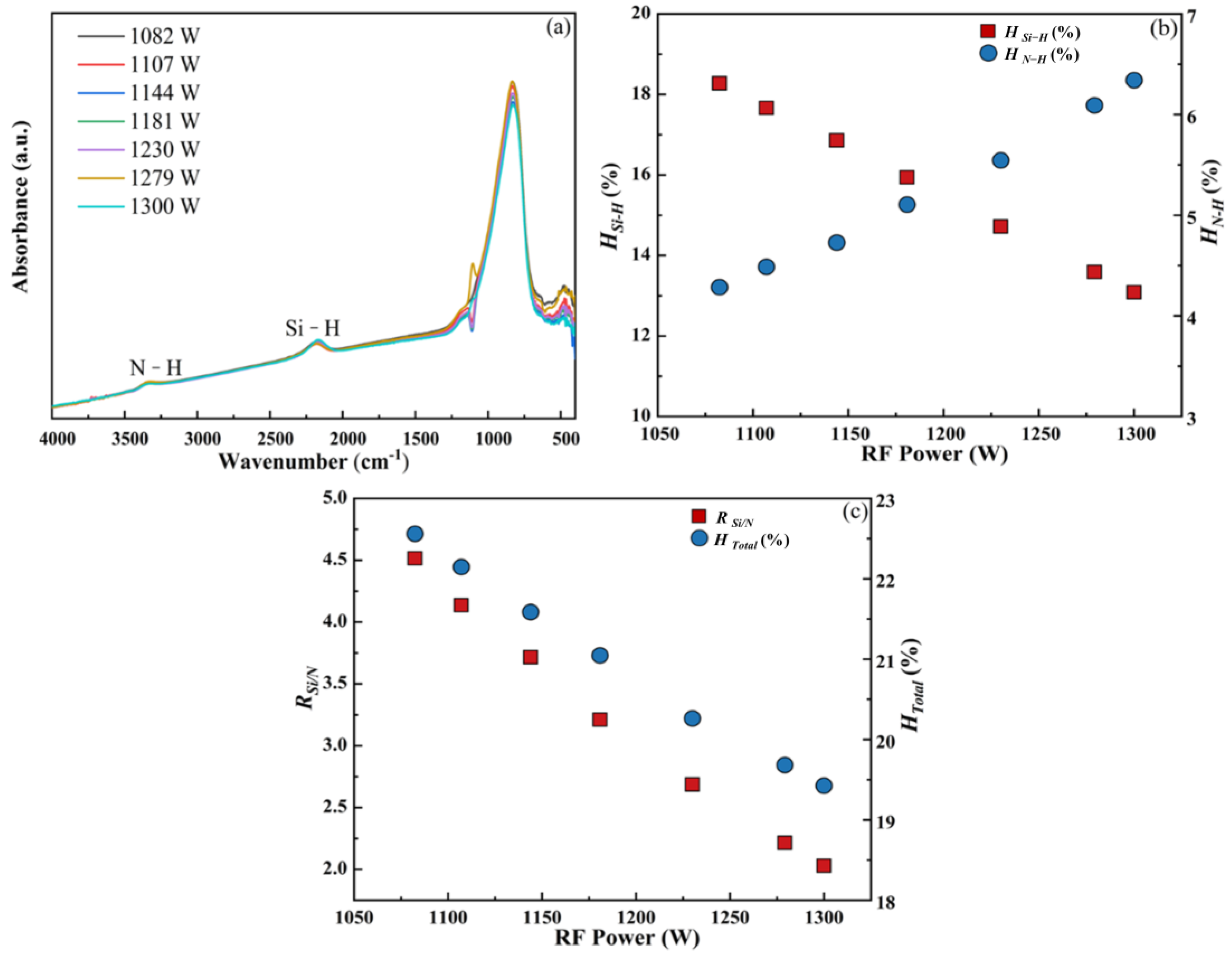
For SiNx:H films, the RI, WERR, stress, and other properties are closely related to the H-related chemical bonds (Si–H and N–H), which are dependent on the deposition conditions [28]. The SiNx:H films deposited under the different conditions exhibited varying HSi–H, HN–H, RSi/N, and HTotal values. To understand how the deposition conditions impacted the film properties by influencing the H-related chemical bonds, in this section, we investigate the effects of the deposition conditions, including the RF power, electrode plate spacing, temperature, chamber pressure, and SiH4:NH3 gas flow ratio, on HSi–H, HN–H, RSi/N, and HTotal.

3.1.1. RF Power

Reactive radicals, ions, neutral atoms, molecules, etc., from reaction gas can be converted by RF power, affecting the atom bonding structures [29]. The FTIR spectra of films deposited under different RF powers are shown in Figure 2a. The absorption peak at ca. 2183 cm−1 is due to the Si–H stretching vibration, while the peak at ca. 3345 cm−1 is ascribed to N–H stretching [30]. According to the FTIR spectra, the HSi–H, HN–H, RSi/N, and HTotal values are as shown in Figure 2b,c. SiH4 and NH3 can be more fully dissociated by increasing the RF power. SiH4 can be easily dissociated into SiH3+, SiH2+, and SiH+; thus, the increase in the RF power mainly promotes the reaction of SiH3+ and SiH2+ dissociation into SiH+. For NH3, the N–H bond energy is higher than the Si–H bond energy (390.8 vs. 318.0 kJ/mol); thus, NH3 dissociation is more difficult than SiH4 dissociation, and the increase in the RF power mainly promotes the dissociation of NH3 [31]. Therefore, as the RF power increases, HSi–H decreases while HN–H increases (Figure 2b), and the decrease in HSi–H is greater than the increase in HN–H. Therefore, as the RF power increases, RSi/N and HTotal decrease.

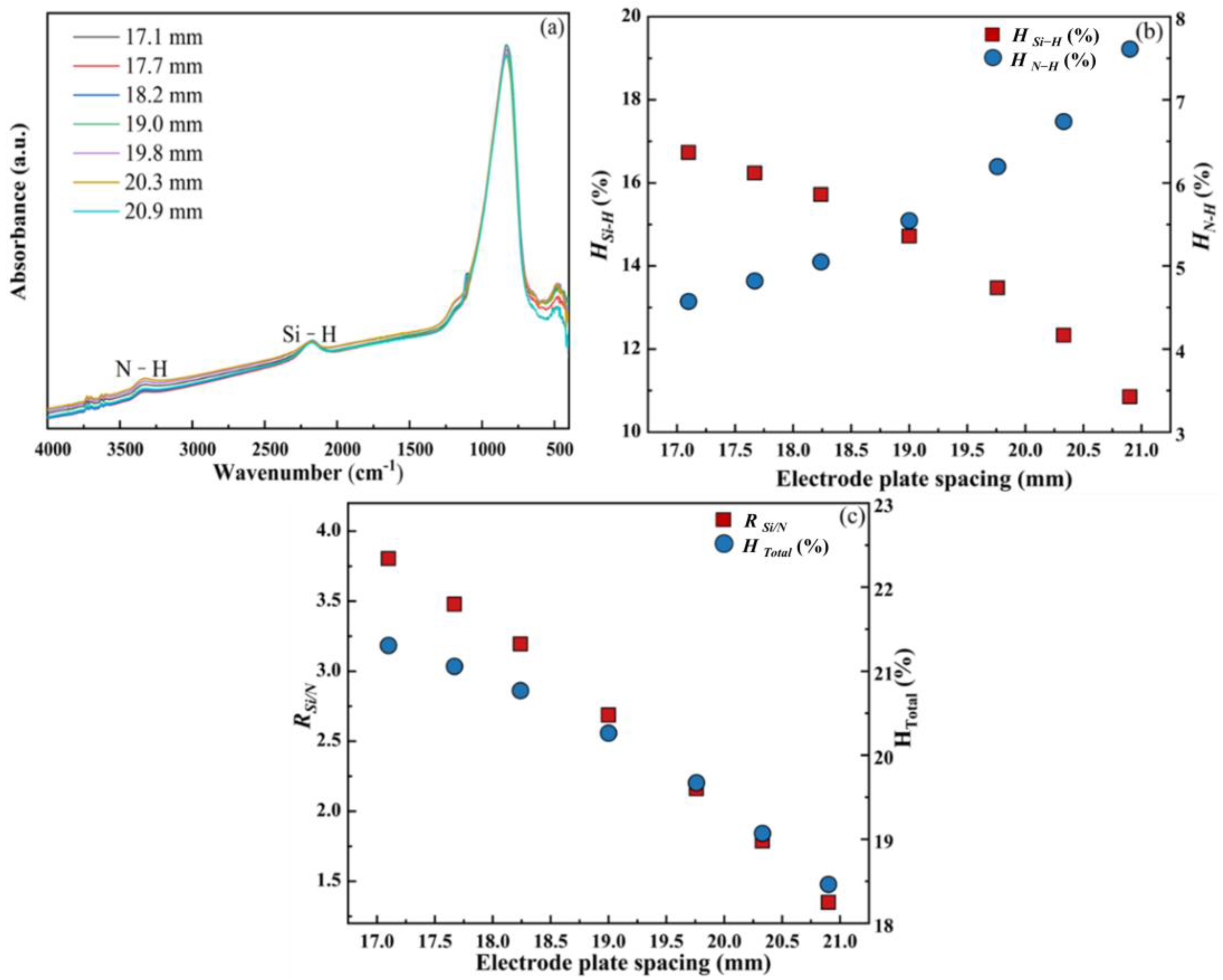
3.1.2. Electrode Plate Spacing

The effect of electrode plate spacing on the FTIR spectra, and the HSi–H, HN–H, RSi/N, and HTotal values, of the films is shown in Figure 3. As the electrode plate spacing increases, the time it takes for SiH4 and NH3 to migrate from the top electrode to the silicon wafer increases, which can lead to a longer SiH4 and NH3 residence time in the electric field and, subsequently, to a fuller dissociation. Thus, like the RF power, the increase in the electrode plate spacing mainly promotes the reaction of SiH3+ and SiH2+ dissociating into SiH+ and the dissociation of NH3. Therefore, as can be seen in Figure 3b,c, as the electrode plate spacing increases, HSi–H decreases while HN–H increases. Meanwhile, the decrease in HSi–H is also greater than that in HN–H. Therefore, as the electrode plate spacing increases, RSi/N and HTotal decrease.

3.1.3. Temperature

Figure 4a shows the FTIR spectra of films under different deposition temperatures. The evolution trends of HSi–H, HN–H, RSi/N, and HTotal with the temperature are plotted in Figure 4b,c. With the increase in the deposition temperature, HSi–H, HN–H, and HTotal decreased, which indicates that Si–H and N–H breakdown can be accelerated by increasing the deposition temperature [32]. Although the N–H bond energy was higher than the Si–H bond energy, as the temperature increased, the downward trend for HSi–H was significantly lower than that for HN–H, and RSi/N increased (Figure 4b,c). The reason for this is that more SiH4 was involved in the film deposition process due to the increased temperature, which made it easier for the Si atoms to bond.

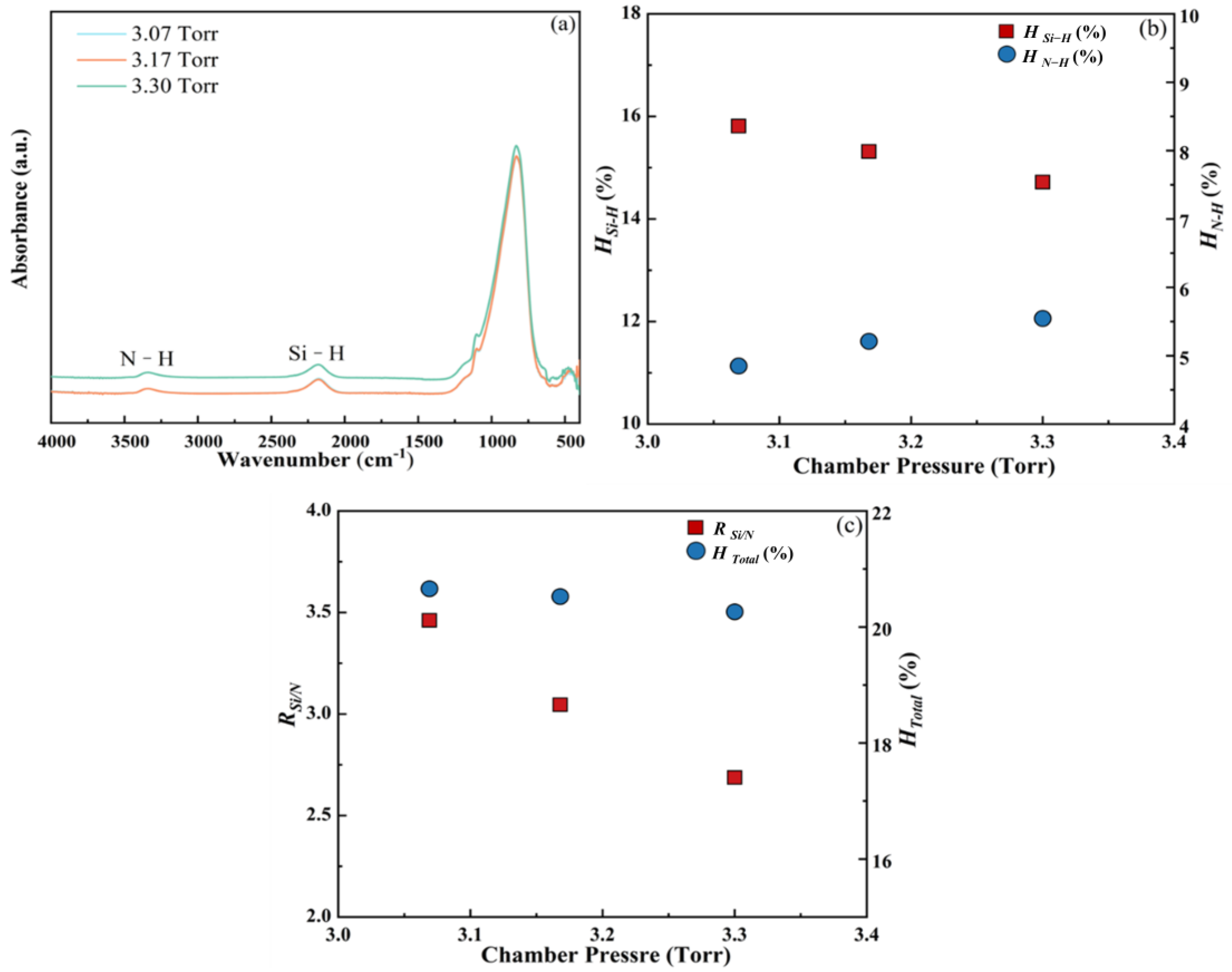
3.1.4. Chamber Pressure

Figure 5a presents the FTIR spectra of films deposited under different pressures. Through the peak areas, the evolution trends of HSi–H, HN–H, RSi/N, and HTotal with the pressure were calculated and are shown in Figure 5b,c. As a result of the chamber pressure increase, the mean free paths of the gases were reduced. This reduction can lead to a decrease in the distance over which the acceleration of molecules, ions, electrons, and other particles occurs [33]. Therefore, as the chamber pressure increases, the energy and activity of these particles are reduced, and the degree of SiH4 and NH3 dissociation decreases. Meanwhile, due to the decrease in the mean free paths of the gas, the bonding of the Si atoms is stronger. Therefore, as the chamber pressure increases, HSi–H decreases, and HN–H and RSi/N increase. The decrease in HSi–H is also greater than the increase in HN–H; thus, HTotal decreases with the increase in the chamber pressure.

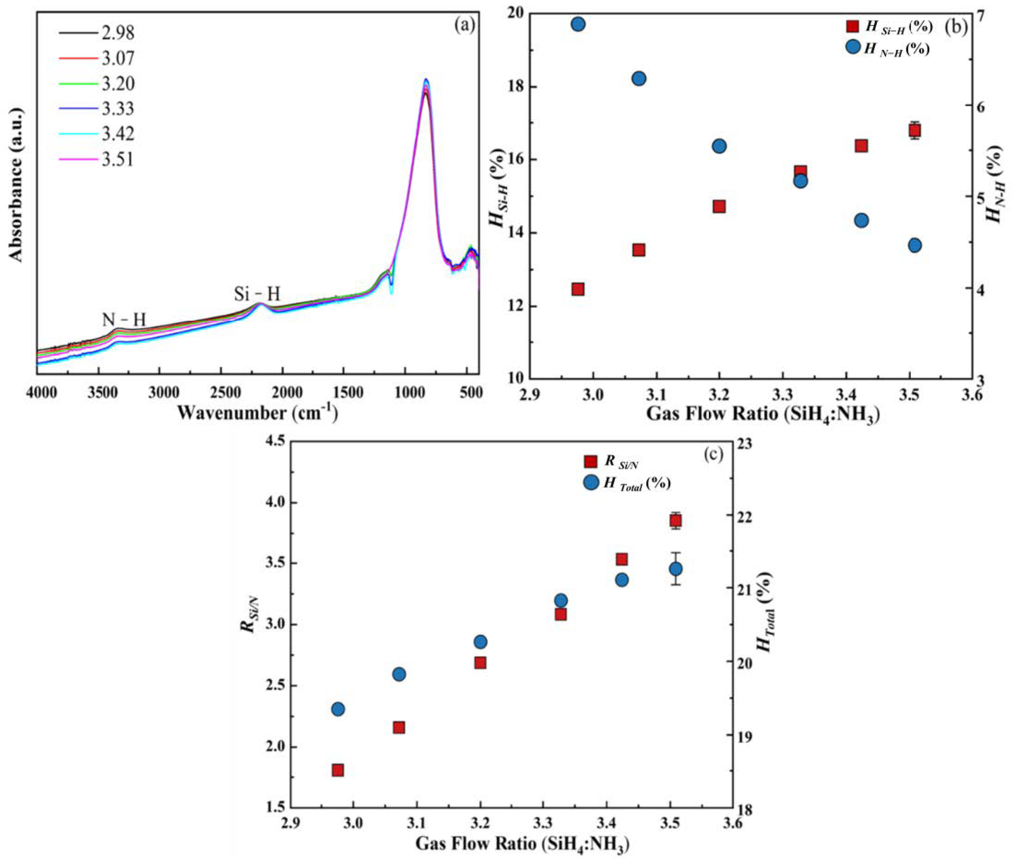
3.1.5. SiH4:NH3 Gas Flow Ratio

We evaluated the impact of the SiH4:NH3 gas flow ratio on the H-related chemical bonds via FTIR, and the results are shown in Figure 6a. Different gas flow ratios were obtained by keeping the NH3 flow constant and adjusting the SiH4 flow. Figure 6b,c show that as the SiH4:NH3 gas flow ratio increased, HSi–H and RSi/N increased, while HN–H decreased. These evolution trends are consistent with previously reported results [31]. Per unit volume, the SiH4 count increased and, accordingly, the NH3 count decreased. Meanwhile, the increase in HSi–H was also greater than the decrease in HN–H; thus, HTotal increased with the increase in the SiH4:NH3 gas flow ratio.

3.2. Influence of Deposition Conditions on SiNx:H Film Properties

The SiNx:H films deposited under different conditions have different HSi–H, HN–H, RSi/N, and HTotal values. The effect mechanisms of H-related chemical bonds on the SiNx:H film properties, including the RI, EB, stress, and WERR, are explored in this section, and some quantitative relationships between the H-related chemical bonds and properties are established. When facing actual production needs, these findings can be used to guide the adjustment directions of the deposition conditions, which can substantially reduce the time and economic costs.

3.2.1. Refractive Index

The RI is an important parameter of the optical properties of films, and it can directly affect the lithography process. The effects of different deposition conditions, including the RF power, electrode plate spacing, temperature, chamber pressure, and gas flow ratio, on the RI of SiNx:H films were explored. As shown in Figure 7a, with an increase in the RF power from 1050 to 1300 W, the RI decreased from 2.100 to 2.028, and with an increase in the electrode plate spacing from 17.1 to 20.9 mm, it decreased from 2.084 to 2.002. Meanwhile, as the RF power or electrode plate spacing increased, RSi/N decreased. In addition, as can be seen in Figure 7b, the RI increased with an increase in temperature. With an increase in temperature from 360 to 440 °C, the RI increased from 2.009 to 2.071. Meanwhile, due to the increase in temperature, the Si atoms bonded more easily to each other, which led to an increase in RSi/N. On the contrary, as the chamber pressure increased, RSi/N decreased. With an increase in the chamber pressure from 3.07 to 3.30 Torr, the RI decreased from 2.065 to 2.044. As can be seen in Figure 7c, as the gas flow ratio increased, RSi/N and the RI increased. With the increase in the gas flow ratio from 2.98 to 3.51, the RI increased from 2.019 to 2.074.
As mentioned above, with the changes in the deposition conditions, the trends for RI and RSi/N were always consistent. To further clarify the relationship between the RI and RSi/N, RI and RSi/N scatter plots are shown in Figure 7d. The fitted linear formula was used to quantitatively describe the relationship between the RI and RSi/N. The correlation coefficient (R2) of this formula was 0.91734, confirming that the RI is related to RSi/N, which indicates that the difference in the RI is mainly due to the change in RSi/N under different deposition conditions. The reason for this is that the relationship between RSi/N and the Si:N atomic ratio is positive and linear, and the Si:N atomic ratio and RI are closely related. When the Si:N atomic ratio increases, the Si–Si bonding of the film increases, and the optical properties become closer to those of amorphous silicon [34,35]. Therefore, the RI increases with an increase in RSi/N. Moreover, the effect of temperature on the RI is more pronounced compared that of to the other deposition conditions, which can be related to Htotal. The networked structure of the film can be interrupted by Si–H and N–H. The lower the Htotal value, the denser the film structure, and the greater the RI. The effect of temperature on Htotal is the greatest among these deposition conditions. As the temperature increases, Htotal decreases and RSi/N increases. Therefore, the RI is the most affected by temperature.

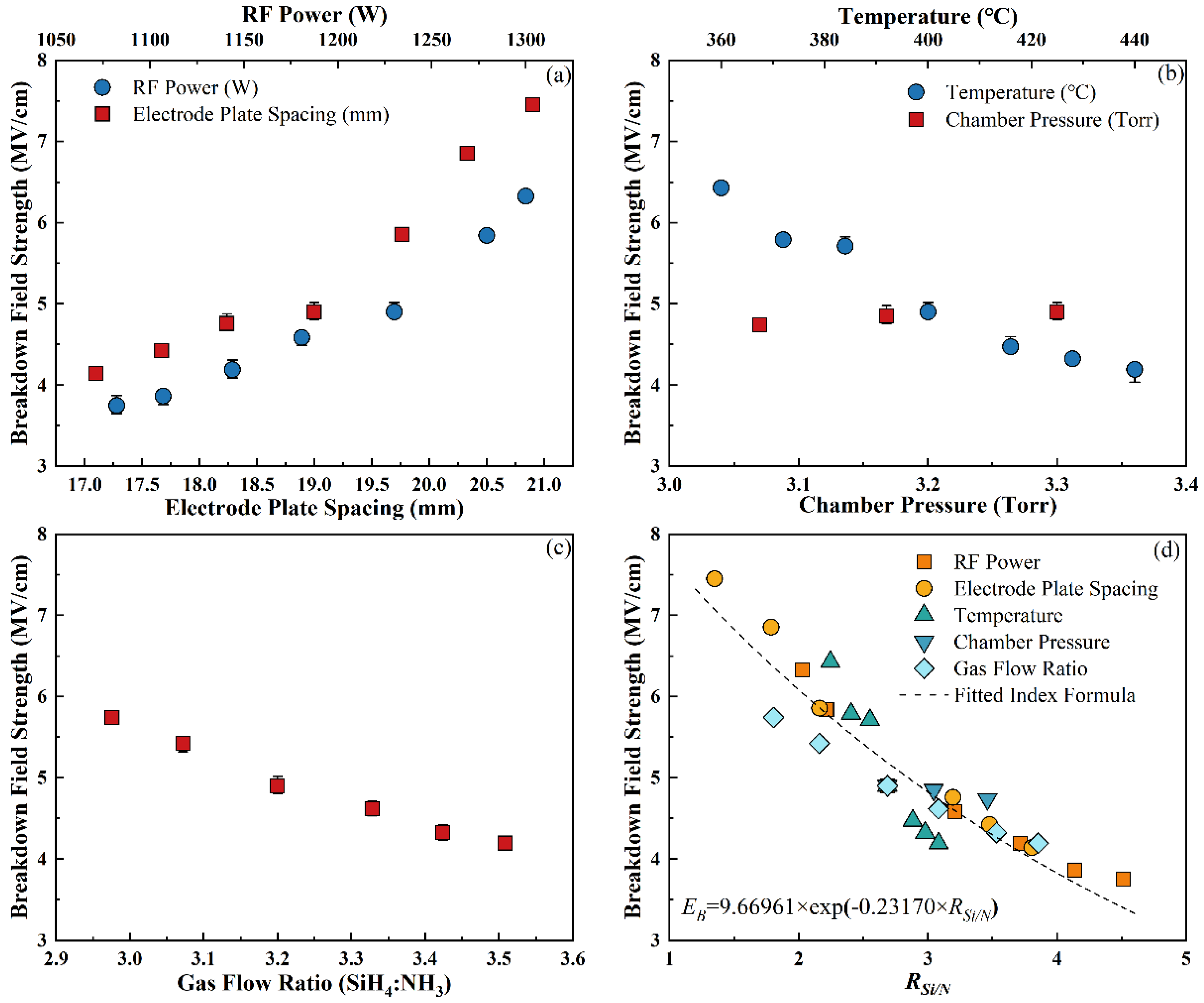
3.2.2. Breakdown Field Strength

The EB value is important for the working performance of SiNx:H film, and it is closely related to the reliability of the IC. The effects of different deposition conditions on the EB of SiNx:H films were explored. As shown in Figure 8a, with an increase in the RF from 1050 to 1300 W, EB increased from 3.75 to 6.33, and with an increase in the electrode plate spacing from 17.1 to 20.9 mm, it increased from 4.14 to 7.45 MV/cm. Correspondingly, as the RF power or electrode plate spacing increased, RSi/N decreased. Moreover, as can be seen in Figure 8b, EB decreased with an increase in temperature and increased with an increase in chamber pressure. With an increase in temperature from 360 to 440 °C, the breakdown voltage decreased from 6.43 to 4.19 MV/cm, and with an increase in chamber pressure from 3.07 to 3.30 Torr, the breakdown voltage increased from 4.74 to 5.10 MV/cm. Moreover, as the temperature increased, RSi/N increased, and as the chamber pressure increased, RSi/N decreased. In addition, with an increase in the gas flow ratio, EB increased and RSi/N decreased. As shown in Figure 8c, with an increase in the gas flow ratio from 2.98 to 3.51, the breakdown voltage decreased from 5.74 to 4.20 MV/cm.
Unlike the RI, with the changes in the deposition conditions, the trends for EB and RSi/N were always opposite. As RSi/N increased, EB decreased. To further explore their relationship, EB and RSi/N scatter plots are shown in Figure 8d. The fitted index formula was used to quantitatively describe the relationship between EB and RSi/N. The correlation coefficient (R2) of this formula was 0.85614, confirming that the difference in EB was also mainly due to the change in RSi/N under different deposition conditions. The reason for this is that as RSi/N decreases, the bandgap width increases, increasing EB [36,37]. In addition, temperature has a more obvious impact on EB, which is also related to Htotal [38]. The suspension bonds and other defects in the film can lead to a decrease in EB, which can be reduced via the introduction of hydrogen [39]. When the deposition temperature increases, Htotal decreases, and the trap density and gap state density in the film increase.

3.2.3. Stress

The stress of the film, which indicates the degree of wafer warping, is primarily divided into intrinsic stress and thermal stress. Intrinsic stress is generated during the deposition process and may be introduced due to lattice mismatch, crystal defects, differences in the unit cell parameters, etc., making it difficult to quantify [40]. Meanwhile, the films deposited via PECVD are all SiNx:H films; thus, the difference in the intrinsic stresses of the films under different deposition conditions is limited. Therefore, the changes in film stress under varying deposition conditions are mainly due to thermal stress, which is influenced by the temperature and can be quantified. The thermal stress (σT) can be calculated using Equation (11) [41]:
σ T = E f 1 V f T D e p T R ( α S α f ) d T
where Ef and Vf are the Young’s modulus and Poisson’s ratio of the film, respectively; TDep and TR are the deposition temperature and test temperature of the film, respectively; αs and αf are the thermal expansion coefficients of the silicon wafers and films, respectively.
As can be seen from Equation (11), σT, TDep and αf are the critical parameters. In this section, the effects of different deposition conditions on the stresses of SiNx:H films are discussed. As shown in Figure 9, the stresses of all the films were negative and were compressive stress. The reason for this is that αf was lower than αs, and the shrinkage of the silicon wafer was greater than that of the film during the cooling process [40].
Under different RF powers, electrode plate spacings, chamber pressures, and gas flow ratios, TDep was the same; thus, the change in the stress can be mainly attributed to the change in αf. αf is related to the degree of structure compactness: The denser the film structure, the lower the αf value and the stress. As can be seen in Figure 9a, as the RF power increased, the stress gradually decreased. With an increase in RF power from 1082 to 1300 W, the stress decreased from −45 to −333 MPa. The reason for this is that as the RF power increases, the molecules are more thoroughly dissociated, and the migration capacity of the active groups increases.
As a result, the structure of the film becomes denser with reduced αf and stress. Unlike the RF power, as the electrode plate spacing increases, so does the stress of the film. With an increase in electrode plate spacing from 17.1 to 20.9 mm, the stress increased from −308 to −156 MPa. The reason for this may be that the distance from the wafer surface to the pumping pipeline was increased by the increased electrode plate spacing, which caused a delay in the pumping of the byproducts away from the wafer surface. An increase in the concentration of byproducts on the wafer surface leads to a decrease in the concentration of reactants, which can cause the structure of the film to become loose.
As shown in Figure 9b, the stress increased with an increase in chamber pressure. With an increase in chamber pressure from 3.07 to 3.30 Torr, the stress increased from −280 to −214 MPa. The reason for this is that the mean free path of the reactants was reduced with increasing pressure, and the diffusion of the reactants was restricted. Therefore, the film structure became loose and αf increased. Additionally, as can also be seen in Figure 9c, as the gas flow ratio increased, the stress also increased. With an increase in the gas flow ratio from 298 to 3.51, the stress increased from −305 to −201 MPa, which indicates that αf increases with the increase in the gas flow ratio.
Under different deposition temperatures, the film stress was related to TDep and αf. The migration capacity of the active groups can be increased by increasing the temperature, which can cause the film structure to become dense and αf to decrease. The film stress increased with an increase in TDep but decreased with a decrease in αf. As shown in Figure 9b, the stress decreased with an increase in temperature, which indicates that the decrease in αf played a predominant role. With an increase in temperature from 360 to 440 °C, the stress decreased from −156 to −342 MPa.
Some previous research results showed that the higher the HTotal value, the looser the film structure and the greater the stress [42,43]. To verify this conclusion, we also explored the relationship between HTotal and stress in this research. However, unlike in previous studies, the stress did not increase with elevated HTotal (Figure 9d), which indicates that the loose films were caused not by the increase in HTotal but by other factors, such as the decrease in the reactant diffusion capacity.

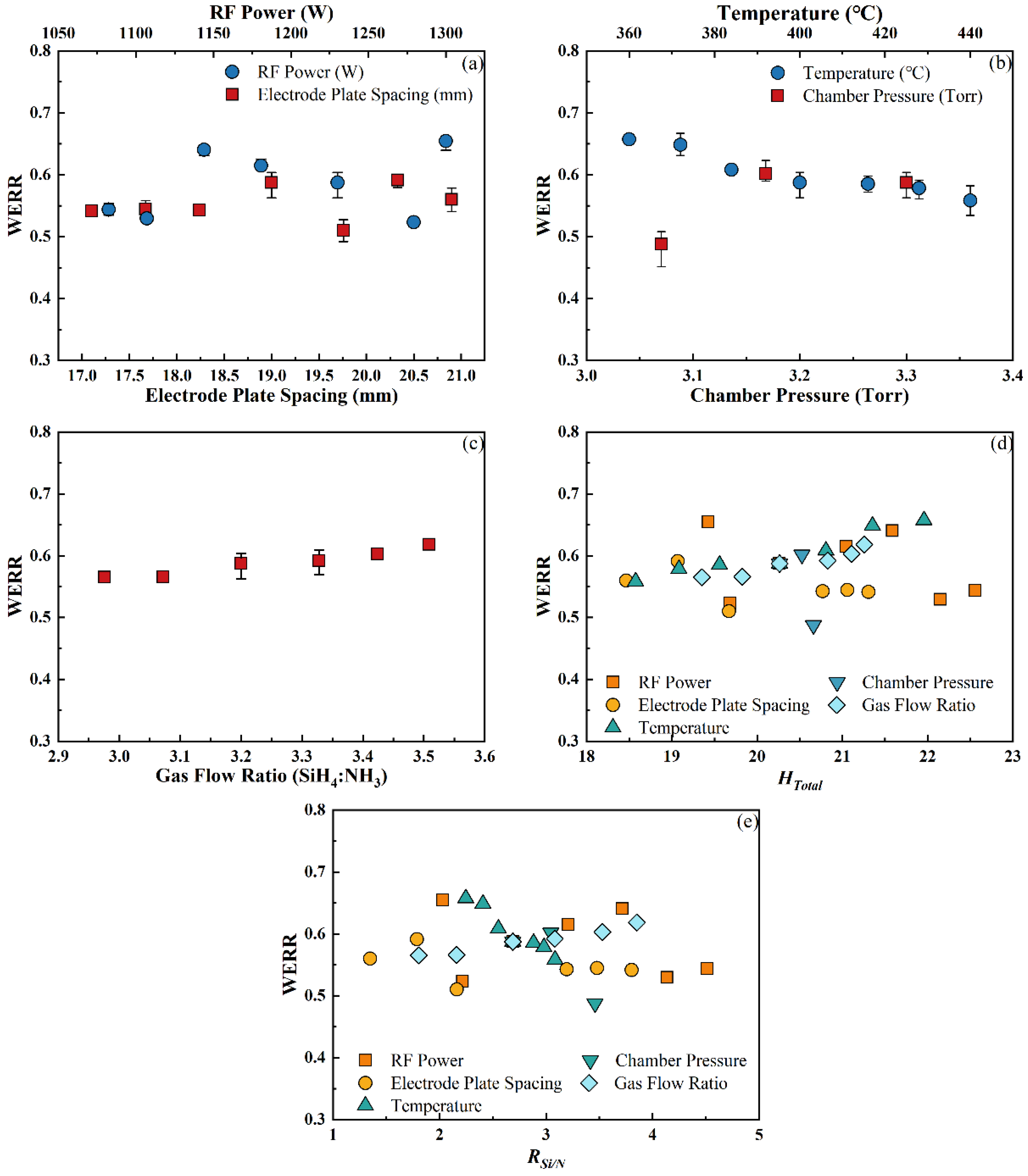
3.2.4. Wet Etching Rate Ratio

We explored the effects of different deposition conditions on the WERR of SiN:H film, which is related to RSi/N and HTotal [44]. As can be seen in Figure 10a, the WERR does not show a constant upward or downward trend with an increase in RF power or electrode plate spacing, which is because RSi/N and HTotal decrease with an increase in the RF power and electrode plate spacing. As RSi/N decreases, the WERR increases. However, HTotal decreases with the decreasing WERR [45]. Therefore, the WERR tends to fluctuate with increases in the RF power and electrode plate spacing.
RSi/N increased while HTotal decreased with the temperature. Therefore, as shown in Figure 10b, the WERR shows a downward trend. With an increase in temperature from 360 to 440 °C, the WERR decreased from 0.66 to 0.56. Unlike the temperature, the WERR shows a fluctuating trend with an increase in chamber pressure. The reason for this is that RSi/N and HTotal decreased with the increase in chamber pressure.
In addition, as can be seen in Figure 10c, as the gas flow ratio increased, both RSi/N and HTotal increased, and the WERR shows an upward rather than fluctuating trend. This indicates that, compared with the increase in RSi/N, the increase in HTotal played the dominant role. With an increase in the gas flow ratio from 2.98 to 3.51, the WERR increased from 0.57 to 0.62. The relationships between HTotal and WERR and between RSi/N and WERR are shown in Figure 10d,e, respectively. In general, compared with RSi/N, HTotal had a greater impact on the WERR of the SiNx:H film.

3.3. Influence of Deposition Conditions on Yield and Quality

For actual production, in addition to the properties, the yield and quality of SiNx:H films are crucial, as they directly affect the product’s profitability [46,47]. The SiNx:H films deposited via PECVD in this research can be used in actual production, necessitating considerations of their yield and quality. Therefore, the effects of different deposition conditions on the deposition rate, non-uniformity, and surface roughness of SiNx:H films were explored as follows.

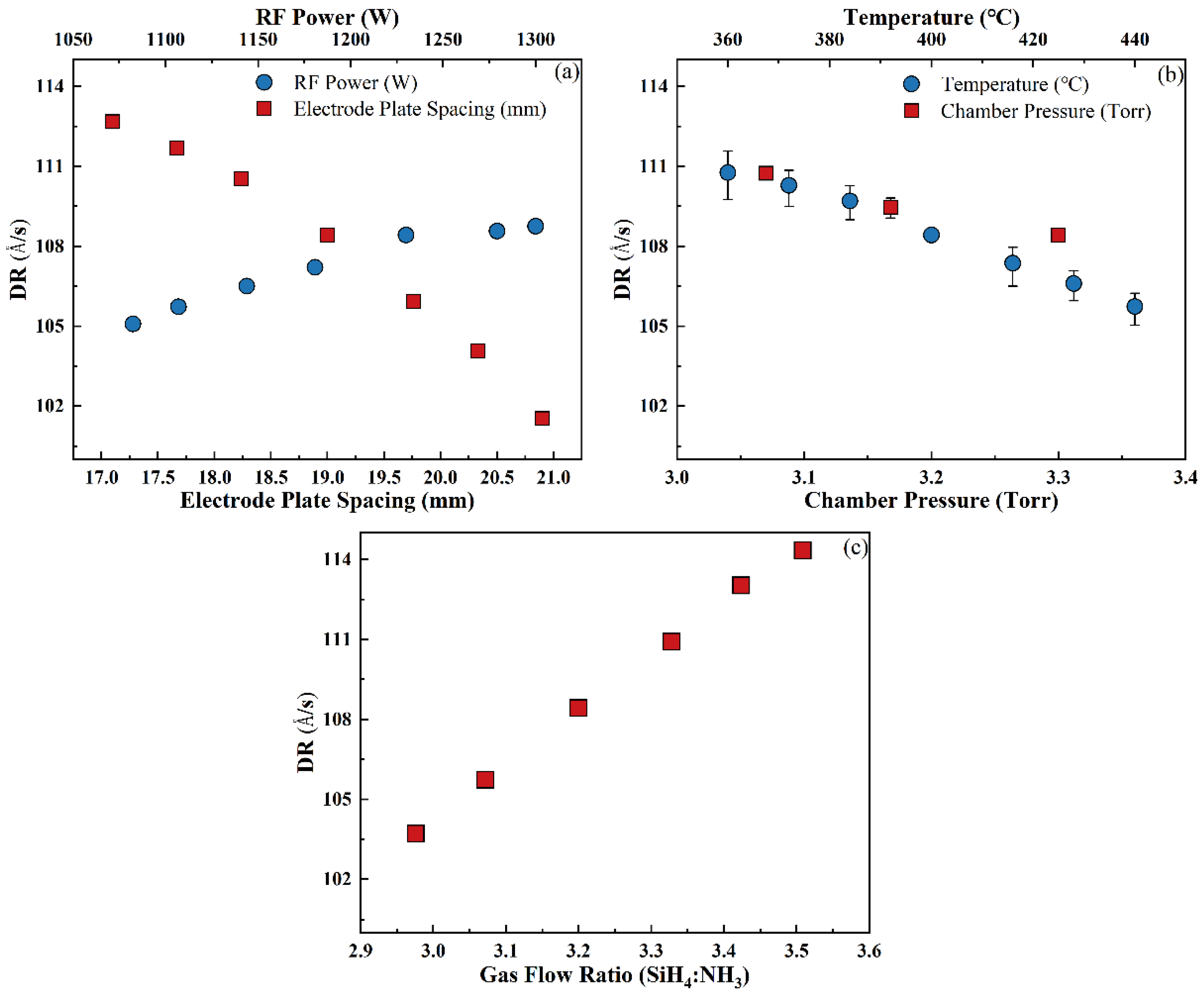
3.3.1. Deposition Rate

The DR is closely related to the film yield. The effects of different deposition conditions on the DR of SiN:H film were explored and are shown in Figure 11. With an increase in RF power from 1082 to 1300 W, the DR increased from 105.09 to 108.76 Å/s (Figure 11a). The reason for this is that the increase in RF power can cause more molecules to detach from the plasma and increase the plasma collision, thereby improving the DR [48]. On the contrary, with an increase in electrode plate spacing from 17.1 to 20.9 mm, the DR decreased from 112.67 to 101.54 Å/s. A possible reason for this is that the increase in the concentration of byproducts on the wafer surface led to a decrease in the concentration of reactants, as discussed in Section 3.2.3.
The effects of temperature and chamber pressure on the DR are shown in Figure 11b. As the chamber pressure increased, the concentration of reactants increased but the DR decreased. With an increase in chamber pressure from 3.07 to 3.30 Torr, the DR decreased from 110.74 to 108.42 Å/s, which was related to the reduction in the reactant migration capacity caused by increasing chamber pressure. Similar to the chamber pressure, as the temperature increases, the reactant energy and reaction rate increase but the DR decreases [49]. With an increase in temperature from 360 to 440 °C, the DR decreased from 110.77 to 105.74 Å/s. The probable reason for this is that the reactant migration capacity on the surface of the silicon wafer can also be increased by increasing the temperature, which can increase the film density [21].
An increase in the gas flow ratio can increase the reactant concentration. The more reactants involved in the reaction per unit time, the higher the DR. Therefore, as shown in Figure 11c, the DR increased with an increase in the gas flow ratio. With an increase in the gas flow ratio from 2.98 to 3.51, the deposition rate increased from 103.71 to 114.55 Å/s.

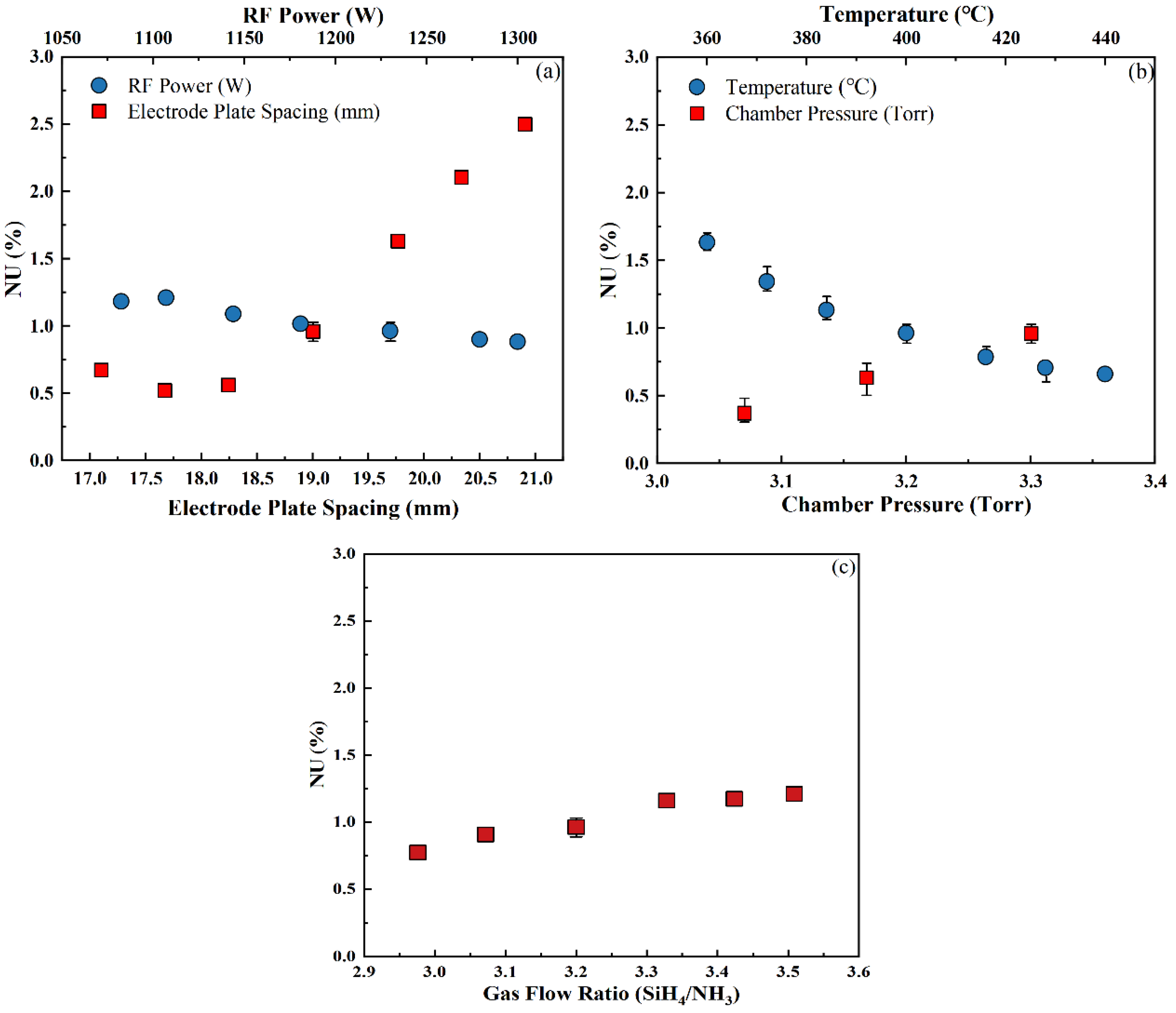
3.3.2. Non-Uniformity

The NU reflects the consistency of the film properties on the entire silicon wafer surface and affects the qualified rate of the product. The effects of different deposition conditions on the NU of SiNx:H films were explored. As can be seen in Figure 12a, as the RF power increases, the NU shows a downward trend, which is related to the increase in the reactant migration capacity caused by increasing the RF power. With an increase in the electrode plate spacing, the NU shows an upward trend, which can be related to the increase in the concentrations of byproducts on the wafer surface and the edge effect of the electric field. As the temperature increases, the reactant migration capacity on the silicon wafer surface increases; thus, the NU decreases. On the contrary, with an increase in chamber pressure, the reactant migration capacity decreases; thus, the NU increases. Meanwhile, as the gas flow ratio increases, the NU increases. In this research, except under large electrode plate spacing and low temperatures, the NU of the SiNx:H films deposited via PECVD was less than 1.5%, which indicates that these films can be used in actual production.

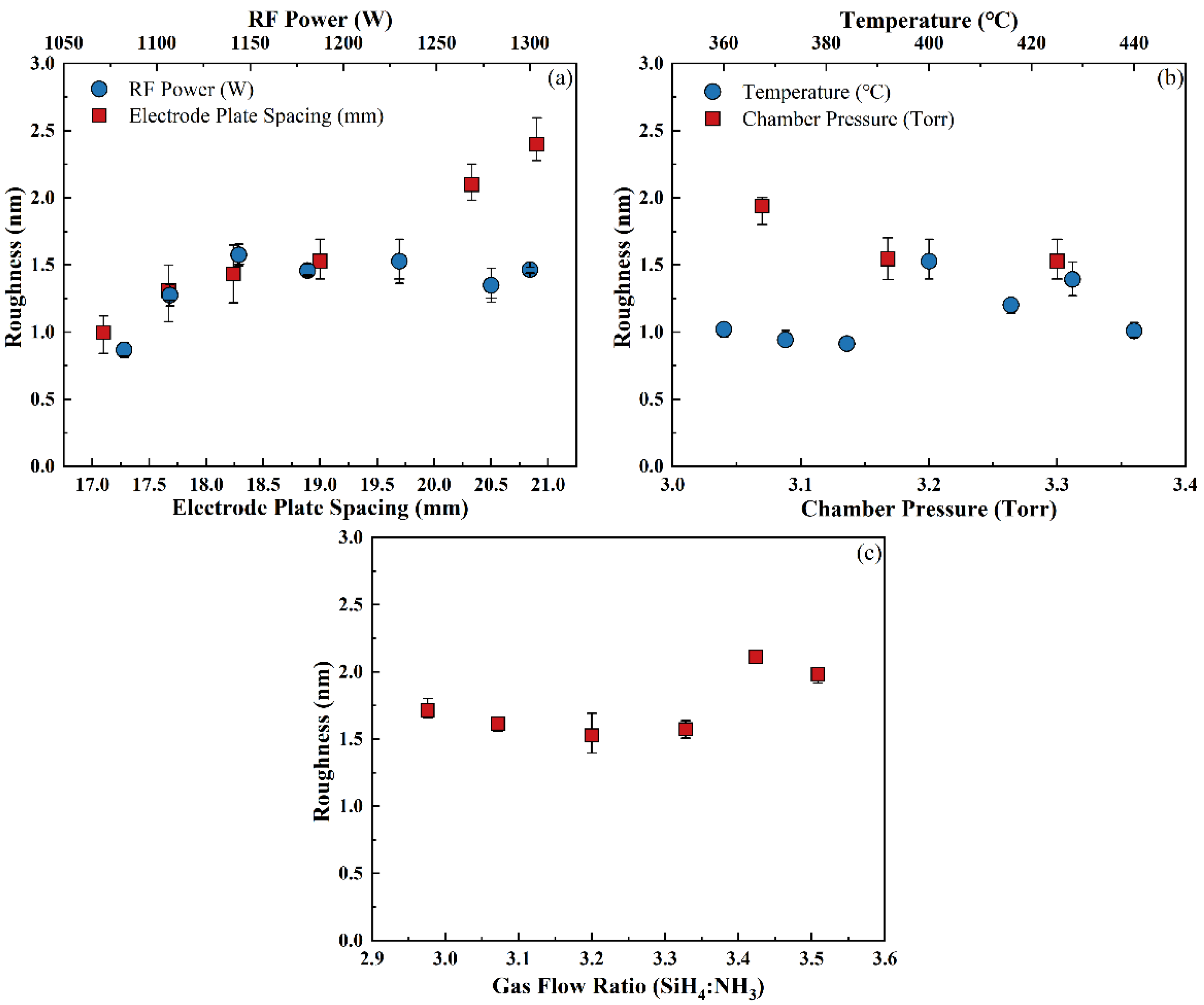
3.3.3. Surface Roughness

The surface roughness reflects a film’s surface situation, and it is also closely related to the quality of the film and product. The lower the roughness, the smoother the surface of the film. The effects of different deposition conditions on the surface roughness and AFM results are shown in Figure 13 and Figure 14, respectively. Among them, the surface roughness of the film deposited under the 20.9 mm electrode plate spacing is the largest, which can also be related to the increase in the concentration of byproducts on the wafer surface. Under the different conditions, most of the deposited films had surface roughness values of less than 2 nm, which indicates that films deposited via PECVD have excellent flatness and can be used in actual production.

4. Conclusions

In this study, SiNx:H films were deposited using mature machines under different deposition conditions. The H-related chemical bonds, RI, EB, stress, WERR, DR, NU, and surface roughness of the films were tested. Based on the test results, we investigated the effects of deposition conditions such as the RF-power, electrode plate spacing, temperature, chamber pressure, and SiH4:NH3 gas flow ratio on the H-related chemical bonds, properties, yield, and quality of SiNx:H films, and the relationships between the H-related chemical bonds and film properties were studied. The conclusions are summarized as follows:
  • Under the different deposition conditions, the differences in the RI and EB can be mainly attributed to the change in RSi/N. Meanwhile, HTotal had a greater impact on the WERR of the SiNx:H films, and the stress was not entirely dependent on HTotal.
  • As RSi/N increased, the RI showed a linear growth trend. The reason for this is that the relationship between RSi/N and the Si:N atomic ratio is positive and linear, and the RI increases with an increase in the Si:N atomic ratio. EB shows an exponential downward trend with an increase in RSi/N, which is related to the decrease in the bandgap width.
  • Excessive electrode plate spacing should be avoided in the development of the deposition process, as it can lead to significant increases in the NU and surface roughness, reducing the product quality.
In conclusion, the study highlights the critical film properties of SiNx:H for semiconductor applications. The reflective index reflects the differences in the composition and microstructure and directly affects the lithography process. The breakdown field strength is electrically related to IC reliability, while film stress impacts the binding force between film layers and radio frequency electric field distribution. Additionally, the yield and quality of SiNx:H films are paramount for production efficiency and economic viability. These findings offer valuable insights for the optimization of semiconductor manufacturing processes.

Author Contributions

J.N.: writing, literature search, study design, data analysis, and interpretation. Z.T.: literature search and writing. L.C.: data collection and analysis. B.L.: writing and data analysis. Q.W.: data collection and analysis. Y.S.: data analysis. D.Z.: study design, data analysis, and literature search. All authors have read and agreed to the published version of the manuscript.

Funding

This research received no external funding.

Data Availability Statement

The data presented in this study are available upon request from the corresponding author.

Acknowledgments

This project was supported by Piotech Technology Co., Ltd. and includes film deposition and film property measurements.

Conflicts of Interest

Author Jianping Ning, Zhen Tang, Lunqian Chen, Bowen Li, Qidi Wu were employed by the company Piotech Inc. The remaining authors declare that the research was conducted in the absence of any commercial or financial relationships that could be construed as a potential conflict of interest.

References

  1. Schurink, B.; van den Beld, W.T.E.; Tiggelaar, R.M.; van de Kruijs, R.W.E.; Bijkerk, F. Synthesis and Characterization of Boron Thin Films Using Chemical and Physical Vapor Depositions. Coatings 2022, 12, 685. [Google Scholar] [CrossRef]
  2. Pecora, A.; Maiolo, L.; Fortunato, G.; Caligiore, C. A comparative analysis of silicon dioxide films deposited by ECR-PECVD, TEOS-PECVD and Vapox-APCVD. J. Non-Cryst. Solids 2006, 352, 1430–1433. [Google Scholar] [CrossRef]
  3. Takagi, T.; Takechi, K.; Nakagawa, Y.; Watabe, Y.; Nishida, S. High rate deposition of a-Si:H and a-SiNx:H by VHF PECVD. Vacuum 1998, 51, 751–755. [Google Scholar] [CrossRef]
  4. Park, H.K.; Song, W.S.; Hong, S.J. In Situ Plasma Impedance Monitoring of the Oxide Layer PECVD Process. Coatings 2023, 13, 559. [Google Scholar] [CrossRef]
  5. Tomankova, K.; Kubecka, M.; Rivolta, N.; Cornil, D.; Obrusnik, A. Simulation of a hollow-cathode PECVD process in O2/TMDSO for silicon dioxide deposition—Cross-code validation of 2D plasma model and global plasma model. Surf. Coat. Technol. 2023, 474, 130069. [Google Scholar] [CrossRef]
  6. Kaloyeros, A.E.; Pan, Y.; Goff, J.; Arkles, B. Review-Silicon Nitride and Silicon Nitride-Rich Thin Film Technologies: State-of-the-Art Processing Technologies, Properties, and Applications. ECS J. Solid State Sci. Technol. 2020, 9, 063006. [Google Scholar] [CrossRef]
  7. Jang, W.; Jeon, H.; Song, H.; Kim, H.; Park, J.; Kim, H.; Jeon, H. The effect of plasma power on the properties of low-temperature silicon nitride deposited by RPALD for a gate spacer. Phys. Status Solidi A 2015, 212, 2785–2790. [Google Scholar] [CrossRef]
  8. Cho, T.Y.; Lee, W.J.; Lee, S.J.; Lee, J.H.; Ryu, J.; Cho, S.K.; Choa, S.H. Moisture barrier and bending properties of silicon nitride films prepared by roll-to-roll plasma enhanced chemical vapor deposition. Thin Solid Film. 2018, 660, 101–107. [Google Scholar] [CrossRef]
  9. Chui, K.J.; Ang, K.W.; Chin, H.C.; Shen, C.; Wong, L.Y.; Tung, C.H.; Balasubramanian, N.; Li, M.F.; Samudra, G.S.; Yeo, Y.C. Strained-SOI n-Channel Transistor With Silicon–Carbon Source/Drain Regions for Carrier Transport Enhancement. IEEE Electron Device Lett. 2006, 27, 778–780. [Google Scholar] [CrossRef]
  10. Kaloyeros, A.E.; Jové, F.A.; Goff, J.; Arkles, B. Review—Silicon Nitride and Silicon Nitride-Rich Thin Film Technologies: Trends in Deposition Techniques and Related Applications. ECS J. Solid State Sci. Technol. 2017, 6, P691. [Google Scholar] [CrossRef]
  11. Oh, S.J.; Ma, B.S.; Yang, C.; Kim, T.-S. Intrinsic Mechanical Properties of Free-Standing SiNx Thin Films Depending on PECVD Conditions for Controlling Residual Stress. ACS Appl. Electron. Mater. 2022, 4, 3980–3987. [Google Scholar] [CrossRef]
  12. Subhani, K.N.; Remesh, N.; Niranjan, S.; Raghavan, S.; Muralidharan, R.; Nath, D.N.; Bhat, K.N. Nitrogen rich PECVD silicon nitride for passivation of Si and AlGaN/GaN HEMT devices. Solid-State Electron. 2021, 186, 108188. [Google Scholar] [CrossRef]
  13. Cao, Y.; Zhou, J.; Ren, Y.; Xu, W.; Liu, W.; Cai, X.; Zhao, B. Study on effect of process and structure parameters on SiNxHy growth by in-line PECVD. Sol. Energy 2020, 198, 469–478. [Google Scholar] [CrossRef]
  14. So, S.J.; Oh, D.S.; Sung, H.K.; Park, C.B. Fabrication of MIM capacitors with 1000 A silicon nitride layer deposited by PECVD for InGaP/GaAs HBT applications. J. Cryst. Growth 2005, 279, 341–348. [Google Scholar] [CrossRef]
  15. Huang, H.; Winchester, K.J.; Suvorova, A.; Lawn, B.R.; Liu, Y.; Hu, X.Z.; Dell, J.M.; Faraone, L. Effect of deposition conditions on mechanical properties of low-temperature PECVD silicon nitride films. Mater. Sci. Eng. A-Struct. Mater. Prop. Microstruct. Process. 2006, 435, 453–459. [Google Scholar] [CrossRef]
  16. Seo, H.; Jung, J.-D. The Silicon Nitride Films according to The Frequency Conditions of Plasma Enhanced Chemical Vapor Deposition. J. Semicond. Disp. Technol. 2014, 13, 21–25. [Google Scholar]
  17. Beliaev, L.Y.; Shkondin, E.; Lavrinenko, A.V.; Takayama, O. Optical, structural and composition properties of silicon nitride films deposited by reactive radio-frequency sputtering, low pressure and plasma-enhanced chemical vapor deposition. Thin Solid Film. 2022, 763, 139568. [Google Scholar] [CrossRef]
  18. Barrera-Mendivelso, E.S.; Rodriguez-Gomez, A. Thin films of silicon nitride deposited at room temperature by non-reactive magnetron sputtering: Radiofrequency power and deposition time influence on the formation of a-Si3N4 and its optical properties. Front. Phys. 2023, 11, 1260579. [Google Scholar] [CrossRef]
  19. Ahn, S.; Hong, S.J.; Yang, H.S.; Cho, S.M. Effect of 2 MHz frequency power applied to the substrate for low-temperature silicon nitride thin film deposition. Mater. Sci. Semicond. Process. 2022, 143, 106538. [Google Scholar] [CrossRef]
  20. Bucio, T.D.; Khokhar, A.Z.; Lacava, C.; Stankovic, S.; Mashanovich, G.Z.; Petropoulos, P.; Gardes, F.Y. Material and optical properties of low-temperature NH3-free PECVD SiNx layers for photonic applications. J. Phys. D-Appl. Phys. 2017, 50, 025106. [Google Scholar] [CrossRef]
  21. Huang, W.D.; Wang, X.H.; Sheng, M.; Xu, L.Q.; Stubhan, F.; Luo, L.; Feng, T.; Wang, X.; Zhang, F.M.; Zou, S.C. Low temperature PECVD SiNx films applied in OLED packaging. Mater. Sci. Eng. B-Solid State Mater. Adv. Technol. 2003, 98, 248–254. [Google Scholar] [CrossRef]
  22. Yang, L.-Q.; Zhang, C.; Li, W.-L.; Liu, G.-H.; Wu, M.; Liu, J.-Q.; Zhang, J.-H. Global optimization of process parameters for low-temperature SiNx based on orthogonal experiments. Adv. Manuf. 2022, 11, 181–190. [Google Scholar] [CrossRef]
  23. Lee, C.-C.; Liou, Y.-Y.; Chang, C.-P.; Huang, P.-C.; Huang, C.-Y.; Chen, K.-C.; Lin, Y.-J. Estimated approach development and experimental validation of residual stress-induced warpage under the SiNx PECVD coating process. Surf. Coat. Technol. 2022, 434, 128225. [Google Scholar] [CrossRef]
  24. Hsiao, S.-N.; Britun, N.; Nguyen, T.-T.-N.; Sekine, M.; Hori, M. Etching Mechanism Based on Hydrogen Fluoride Interactions with Hydrogenated SiN Films Using HF/H2 and CF4/H2 Plasmas. ACS Appl. Electron. Mater. 2023, 5, 6797–6804. [Google Scholar] [CrossRef]
  25. Yang, X.; Wu, M.; Jian, M.; Zhu, S.; Jiang, J.; Yang, L. Feasibility of molecular dynamics simulation for process parameter guidance of silicon nitride thin films by PECVD. Appl. Surf. Sci. 2024, 654, 159401. [Google Scholar] [CrossRef]
  26. Kovačević, G.; Pivac, B. Reactions in silicon–nitrogen plasma. Phys. Chem. Chem. Phys. 2017, 19, 3826–3836. [Google Scholar] [CrossRef] [PubMed]
  27. Thomas, R.; Benoit, D.; Clément, L.; Morin, P.; Cooper, D.; Bertin, F. Characterization of Strain Induced by PECVD Silicon Nitride Films in Transistor Channels. AIP Conf. Proc. 2011, 1395, 90–94. [Google Scholar] [CrossRef]
  28. Kamataki, K.; Sasaki, Y.; Nagao, I.; Yamashita, D.; Okumura, T.; Yamashita, N.; Itagaki, N.; Koga, K.; Shiratani, M. Low-temperature fabrication of silicon nitride thin films from a SiH4+N2 gas mixture by controlling SiNx nanoparticle growth in multi-hollow remote plasma chemical vapor deposition. Mater. Sci. Semicond. Process. 2023, 164, 107613. [Google Scholar] [CrossRef]
  29. Sciammarella, C.A.; Boccaccio, A.; Lamberti, L.; Pappalettere, C.; Rizzo, A.; Signore, M.A.; Valerini, D. Measurements of Deflection and Residual Stress in Thin Films Utilizing Coherent Light Reflection/Projection Moir, Interferometry. Exp. Mech. 2013, 53, 977–987. [Google Scholar] [CrossRef]
  30. Mao, S.C.; Tao, S.H.; Xu, Y.L.; Sun, X.W.; Yu, M.B.; Lo, G.Q.; Kwong, D.L. Low propagation loss SiN optical waveguide prepared by optimal low-hydrogen module. Opt. Express 2008, 16, 20809–20816. [Google Scholar] [CrossRef]
  31. Jehanathan, N. Thermal Stability of Plasma Enhanced Chemical Vapor Deposition Silicon Nitride Thin Films. Master’s Thesis, The University of Western Australia, Perth, Australia, 2007. [Google Scholar]
  32. Jiang, L.; Tian, H.; Li, J.; Xiang, P.; Peng, Y.; Wang, T.; Hou, P.; Xiao, T.; Tan, X. The influence of NH3 flow rate on the microstructure and oxidation properties of a-Si-C-N:H films prepared by PECVD technology. Appl. Surf. Sci. 2020, 513, 145861. [Google Scholar] [CrossRef]
  33. Xu, X.; He, Q.; Fan, T.; Jiang, Y.; Huang, L.; Ao, T.; Ma, C. Hard and relaxed a-SiNxHy films prepared by PECVD: Structure analysis and formation mechanism. Appl. Surf. Sci. 2013, 264, 823–831. [Google Scholar] [CrossRef]
  34. Bakardjieva, V.; Beshkova, G.; Vitanov, P.; Alexieva, Z. Effect of rapid thermal annealving on the properties of µPCVD and PECVD silicon nitride thin films. J. Optoelectron. Adv. Mater. 2005, 7, 377–380. [Google Scholar]
  35. Zhou, J.; Huang, J.; Liao, J.; Guo, Y.; Zhao, Z.; Liang, H. Multi-field simulation and optimization of SiNx:H thin-film deposition by large-size tubular LF-PECVD. Sol. Energy 2021, 228, 575–585. [Google Scholar] [CrossRef]
  36. Benoit, D.; Morin, P.; Regolini, J. Determination of silicon nitride film chemical composition to study hydrogen desorption mechanisms. Thin Solid Film. 2011, 519, 6550–6553. [Google Scholar] [CrossRef]
  37. Mäckel, H.; Lüdemann, R. Detailed study of the composition of hydrogenated SiNx layers for high-quality silicon surface passivation. J. Appl. Phys. 2002, 92, 2602–2609. [Google Scholar] [CrossRef]
  38. Ghosh, S.; Bose, D.N. Plasma-enhanced chemical-vapor-deposited silicon-nitride films for interface studies. J. Mater. Sci. Mater. Electron. 1994, 5, 193–198. [Google Scholar] [CrossRef]
  39. Koutsoureli, M.; Birmpiliotis, D.; Papaioannou, G. A study of material stoichiometry on charging properties of SiNx films for potential application in RF MEMS capacitive switches. Microelectron. Reliab. 2020, 114, 113759. [Google Scholar] [CrossRef]
  40. Inukai, T.I.T.; Ono, K.I.O.K.I. Optical Characteristics of Amorphous Silicon Nitride Thin Films Prepared by Electron Cyclotron Resonance Plasma Chemical Vapor Deposition. Jpn. J. Appl. Phys. 1994, 33, 2593. [Google Scholar] [CrossRef]
  41. Jang, W.; Jeon, H.; Kang, C.; Song, H.; Park, J.; Kim, H.; Seo, H.; Leskela, M.; Jeon, H. Temperature dependence of silicon nitride deposited by remote plasma atomic layer deposition. Phys. Status Solidi 2015, 211, 2166–2171. [Google Scholar] [CrossRef]
  42. Kim, J.G.; Yu, J. Behavior of residual stress on CVD diamond films. Mater. Sci. Eng. B-Solid State Mater. Adv. Technol. 1998, 57, 24–27. [Google Scholar] [CrossRef]
  43. Peng, K.-P.; Kuo, Y.-H.; Chang, L.-H.; Hsiao, C.-N.; Chung, T.-F.; George, T.; Lin, H.-C.; Li, P.-W. Silicon nitride engineering: Role of hydrogen-bonding in Ge quantum dot formation. Semicond. Sci. Technol. 2020, 35, 105018. [Google Scholar] [CrossRef]
  44. Miyagawa, Y.; Murata, T.; Nishida, Y.; Nakai, T.; Uedono, A.; Hattori, N.; Matsuura, M.; Asai, K.; Yoneda, M. Local bonding structure of high-stress silicon nitride film modified by UV curing for strained silicon technology beyond 45 nm node SoC devices. Jpn. J. Appl. Phys. Part 1-Regul. Pap. Brief Commun. Rev. Pap. 2007, 46, 1984–1988. [Google Scholar] [CrossRef]
  45. Barcellona, M.; Samperi, O.; Russo, D.; Battaglia, A.; Fischer, D.; Fragala, M.E. Differences in HF Wet Etching Resistance of PECVD SiNx:H thin films. Mater. Chem. Phys. 2023, 306, 128023. [Google Scholar] [CrossRef]
  46. Jiang, Z.; Zhu, H.; Sun, Q. Process Optimization of Amorphous Carbon Hard Mask in Advanced 3D-NAND Flash Memory Applications. Electronics 2021, 10, 1374. [Google Scholar] [CrossRef]
  47. Kim, D.; Lee, H.; Kim, B.; Seo, Y.H.; Yoon, N.-G.; Han, D. Impact of Duty Ratio-Controlled Ion Energy on Surface Roughness of Silicon Nitride Films Deposited Using a SiH4-NH3 Plasma. J. Nanosci. Nanotechnol. 2011, 11, 5744–5748. [Google Scholar] [CrossRef] [PubMed]
  48. Lee, M.-J.; Kar, J.P.; Lee, T.I.; Lee, D.; Choi, D.-K.; Cho, J.-H.; Myoung, J.-M. Investigation of optical and compositional properties of thin SiNx:H films with an enhanced growth rate by high frequency PECVD method. Vacuum 2011, 85, 1032–1036. [Google Scholar] [CrossRef]
  49. El Amrani, A.; Bekhtari, A.; Mahmoudi, B.; Lefgoum, A.; Menari, H. Experimental study of the effect of process parameters on plasma-enhanced chemical vapour deposition of silicon nitride film. Vacuum 2011, 86, 386–390. [Google Scholar] [CrossRef]
Figure 1. Schematic diagram of the SiNx:H film deposition process.
Electronics 13 02779 g001
Figure 2. Effects of RF power on (a) FTIR spectrum, (b) HSi–H and HN–H, and (c) RSi/N and HTotal.
Electronics 13 02779 g002
Figure 3. Effects of electrode plate spacing on (a) FTIR spectra, (b) HSi–H and HN–H, and (c) RSi/N and HTotal.
Electronics 13 02779 g003
Figure 4. Effects of temperature on (a) FTIR spectrum, (b) HSi–H and HN–H, and (c) RSi/N and HTotal.
Electronics 13 02779 g004
Figure 5. Effects of chamber pressure on (a) FTIR spectrum, (b) HSi–H and HN–H, and (c) RSi/N and HTotal.
Electronics 13 02779 g005
Figure 6. Effects of SiH4:NH3 gas flow ratio on (a) FTIR spectrum, (b) HSi–H and HN–H, and (c) RSi/N and HTotal.
Electronics 13 02779 g006
Figure 7. Effects of different deposition conditions on RI: (a) RF power and electrode plate spacing; (b) temperature and chamber pressure; (c) gas flow ratio; (d) relationship between RSi/N and RI.
Electronics 13 02779 g007
Figure 8. Effects of different deposition conditions on breakdown field strength: (a) RF power and electrode plate spacing; (b) temperature and chamber pressure; (c) gas flow ratio; (d) relationship between RSi/N and breakdown field strength.
Electronics 13 02779 g008
Figure 9. Effects of different deposition conditions on stress: (a) RF power and electrode plate spacing; (b) temperature and chamber pressure; (c) gas flow ratio; (d) relationship between HTotal and stress.
Electronics 13 02779 g009
Figure 10. Effects of different deposition conditions on WERR: (a) RF power and electrode plate spacing; (b) temperature and chamber pressure; (c) gas flow ratio; (d) relationship between HTotal and WERR; (e) relationship between RSi/N and WERR and RF power, electrode plate spacing, temperature, chamber pressure, and gas flow ratio.
Electronics 13 02779 g010
Figure 11. Effects of different deposition conditions on DR: (a) RF power and electrode plate spacing; (b) temperature and chamber pressure; (c) gas flow ratio.
Electronics 13 02779 g011
Figure 12. Effects of different deposition conditions on NU: (a) RF power and electrode plate spacing; (b) temperature and chamber pressure; (c) gas flow ratio.
Electronics 13 02779 g012
Figure 13. Effects of different deposition conditions on surface roughness: (a) RF power and electrode plate spacing; (b) temperature and chamber pressure; (c) gas flow ratio.
Electronics 13 02779 g013
Figure 14. AFM results under different deposition conditions. RF power: (a) 1082 W and (b) 1300 W; electrode plate spacing: (c) 17.1 mm and (d) 20.9 mm; temperature: (e) 360 °C and (f) 440 °C; chamber pressure: (g) 3.07 Torr and (h) 3.30 Torr; gas flow ratio: (i) 2.98 and (j) 3.51.
Electronics 13 02779 g014
Table 1. Basic deposition conditions for SiNx:H films.
Deposition ConditionsRF PowerElectrode Plate SpacingTemperaturePressureSiH4:NH3 Gas Flow Ratio
(W)(mm)(°C)(Torr)
Value123019.04003.303.20
Table 2. Experimental conditions for SiNx:H film deposition.
Deposition ConditionsRF PowerElectrode Plate SpacingTemperaturePressureSiH4:NH3 Gas Flow Ratio
(W)(mm)(°C)(Torr)
Basic123019.04003.303.20
RF
Power
108219.04003.303.20
118019.04003.303.20
114419.04003.303.20
110719.04003.303.20
127919.04003.303.20
130019.04003.303.20
Electrode Plate Spacing123017.14003.303.20
123017.74003.303.20
123018.24003.303.20
123019.84003.303.20
123020.34003.303.20
123020.94003.303.20
Temperature123019.03603.303.20
123019.03723.303.20
123019.03843.303.20
123019.04003.303.20
123019.04163.303.20
123019.04283.303.20
123019.04403.303.20
Pressure123019.04003.073.20
123019.04003.173.20
SiH4:NH3 Gas Flow Ratio123019.04003.302.98
123019.04003.303.07
123019.04003.303.33
123019.04003.303.42
123019.04003.303.51
Disclaimer/Publisher’s Note: The statements, opinions and data contained in all publications are solely those of the individual author(s) and contributor(s) and not of MDPI and/or the editor(s). MDPI and/or the editor(s) disclaim responsibility for any injury to people or property resulting from any ideas, methods, instructions or products referred to in the content.

