Article

Research on Boost-Type Cascaded H-Bridge Inverter and Its Power Control in Photovoltaic Power Generation System

School of Electrical and Control Engineering, Shaanxi University of Science and Technology, Xi’an 710021, China
*
Author to whom correspondence should be addressed.
Electronics 2024, 13(14), 2819; https://doi.org/10.3390/electronics13142819
Submission received: 19 June 2024 / Revised: 14 July 2024 / Accepted: 16 July 2024 / Published: 18 July 2024
(This article belongs to the Section Power Electronics)

Abstract

:
The cascaded H-bridge (CHB) inverter has become pivotal in grid-connected photovoltaic (PV) systems owing to its numerous benefits. Typically, DC–DC converters are employed to boost the input voltage in grid-connected systems to meet the grid’s higher voltage requirements, but this approach increases equipment size and cost. To enhance inverter efficiency, this paper proposes a boost-type, three-phase CHB PV grid-connected inverter. This design can raise the input voltage and satisfy grid requirements with only a few additional components. Additionally, PV environmental fluctuations can cause variations in PV power generation, leading to a power imbalance in the inverter and potentially affecting the stability of the PV system. Based on this, we consider grid voltage fluctuations induced by unbalanced power output from the inverter and propose an improved control method based on the superposition of zero-sequence components. Finally, we construct a simulation model and conduct experimental verification using the MATLAB/Simulink platform. The validation results demonstrate that this topology reduces equipment volume and effectively enhances the efficiency of PV power generation systems. Furthermore, the designed control method ensures system stability while effectively mitigating power imbalances caused by PV module and grid voltage fluctuations.

1. Introduction

The issues of energy and ecology, which are crucial challenges faced by all nations worldwide, are intricately linked to the survival and development of humanity [1,2]. Photovoltaic energy has the characteristics of being clean, renewable, and widely distributed. It can reduce the dependence of modern industry on traditional fossil fuels and promote energy transformation and low-carbon development, which is particularly important in the current context [3,4]. Currently, countries worldwide are researching how to efficiently develop and utilize photovoltaic (PV) energy, with a primary focus on grid-connected photovoltaic systems for electricity generation. As inverters are the energy conversion interface within photovoltaic systems, their performance critically determines the overall system cost [5]. Currently, multi-level inverters are widely employed, with the neutral-point clamped, flying-capacitor [6], and cascade H-bridge (CHB) [7] architectures being the most prevalent. Among these, the cascaded H-bridge (CHB) structure holds significant research and application value due to its features. It has several advantages, such as maximizing the utilization of DC sources, low harmonic content, modular composition, and the ability to output higher levels of voltage.
Presently, research on CHB PV grid-connected systems primarily revolves around: topology structure [8], control strategies [9,10], and modulation methods [11]. The system structure can be divided into single-stage and two-stage configurations. The two-stage structure incorporates a DC/DC converter, which can generate a higher voltage magnitude to meet the grid requirements but may lead to increased costs and energy losses. Additionally, the power imbalance issue with CHB inverters merits consideration [12]. Variations in external conditions and the status of the grid will impact the PV module, leading to an inverter power imbalance [13,14]. This imbalance can distort or imbalance the grid output current. For the aforementioned scenario, a photovoltaic grid-based quasi-Z-source cascaded multilevel inverter was proposed in [15,16]. This approach enhances efficiency by minimizing system size, albeit at the cost of increased computational complexity and a notable oversight in addressing power imbalance. A boost-type CHB structure with a simplified control scheme has been proposed in [17]. However, its scope remains limited to single-phase systems, impeding its extension to three-phase applications and overlooking the crucial issue of power imbalance. A power control method for quasi-Z source CHB grid-connected inverters was proposed in [18], yet it requires modifications for applicability to conventional CHB structures. The inclusion of additional energy storage batteries can assist in achieving power balance control for inverters, as proposed in [19,20,21]. However, this approach introduces additional circuits, thereby elevating overall costs and system complexity.
In response to previous studies, this paper proposes a three-phase, boost-type cascaded H-bridge inverter along with its power balance control strategy. By optimizing the inverter’s topology, higher voltage levels are achieved without additional multi-level structures, enhancing photovoltaic energy conversion efficiency. Moreover, the proposed control strategy effectively achieves power balance in the system. This strategy comprises overall control and power imbalance control, utilizing a voltage-current double closed-loop control loop and a proportional quasi-resonant controller to optimize inverter performance while reducing costs. The system control strategy is researched and designed to handle concurrent cases of power imbalance and grid voltage fluctuations. A power imbalance control module is integrated into the control loop, achieving power balance through zero-sequence voltage computation and superposition. Table 1 illustrates the differences between the proposed content and other inverter structures (focusing solely on one single H-bridge module). Based on the comparison presented in the table, it can be observed that the system proposed in this paper possesses several advantages, including fewer components used, a simpler structural design, a straightforward control strategy, and the ability to cope with various situational changes.

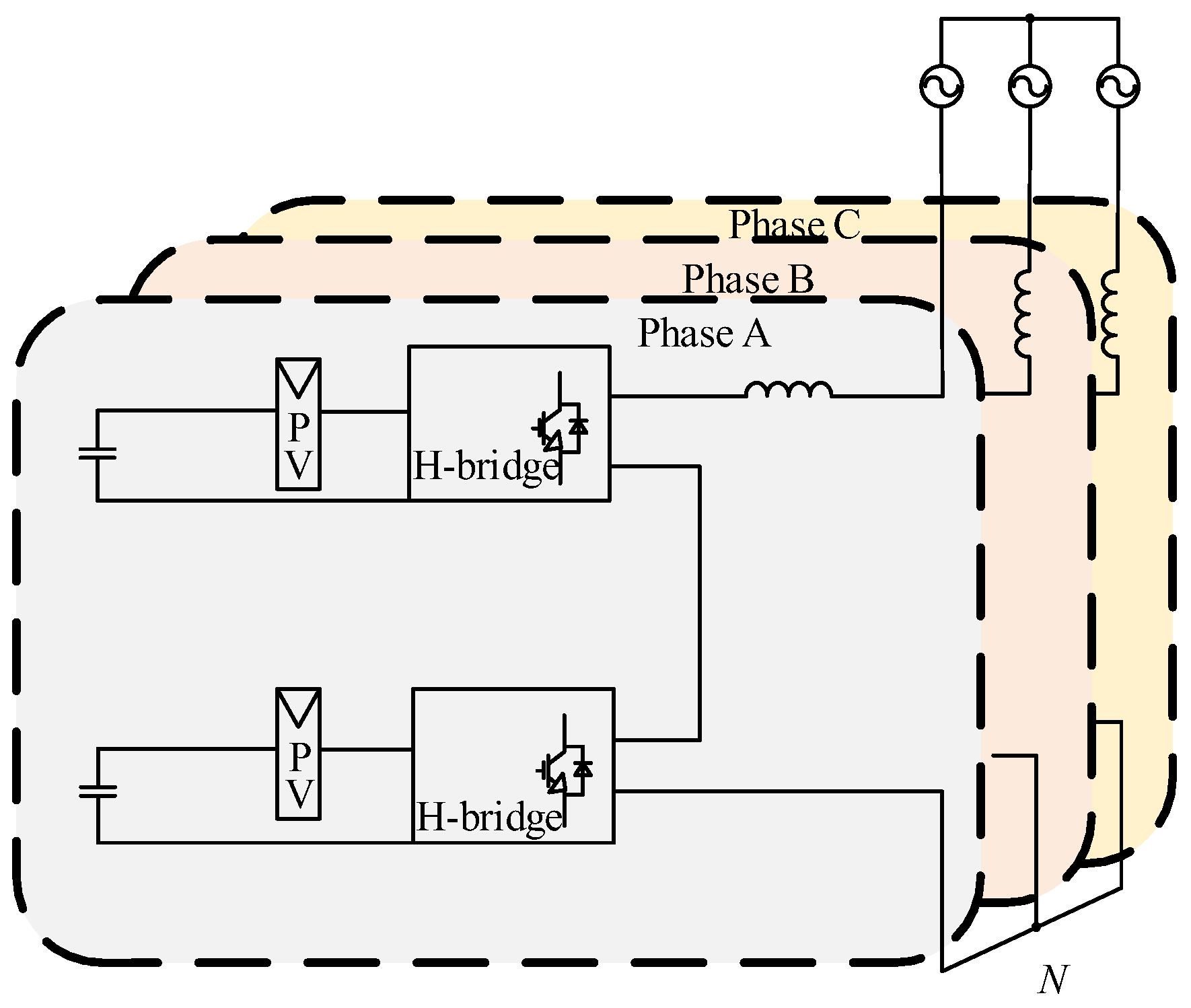
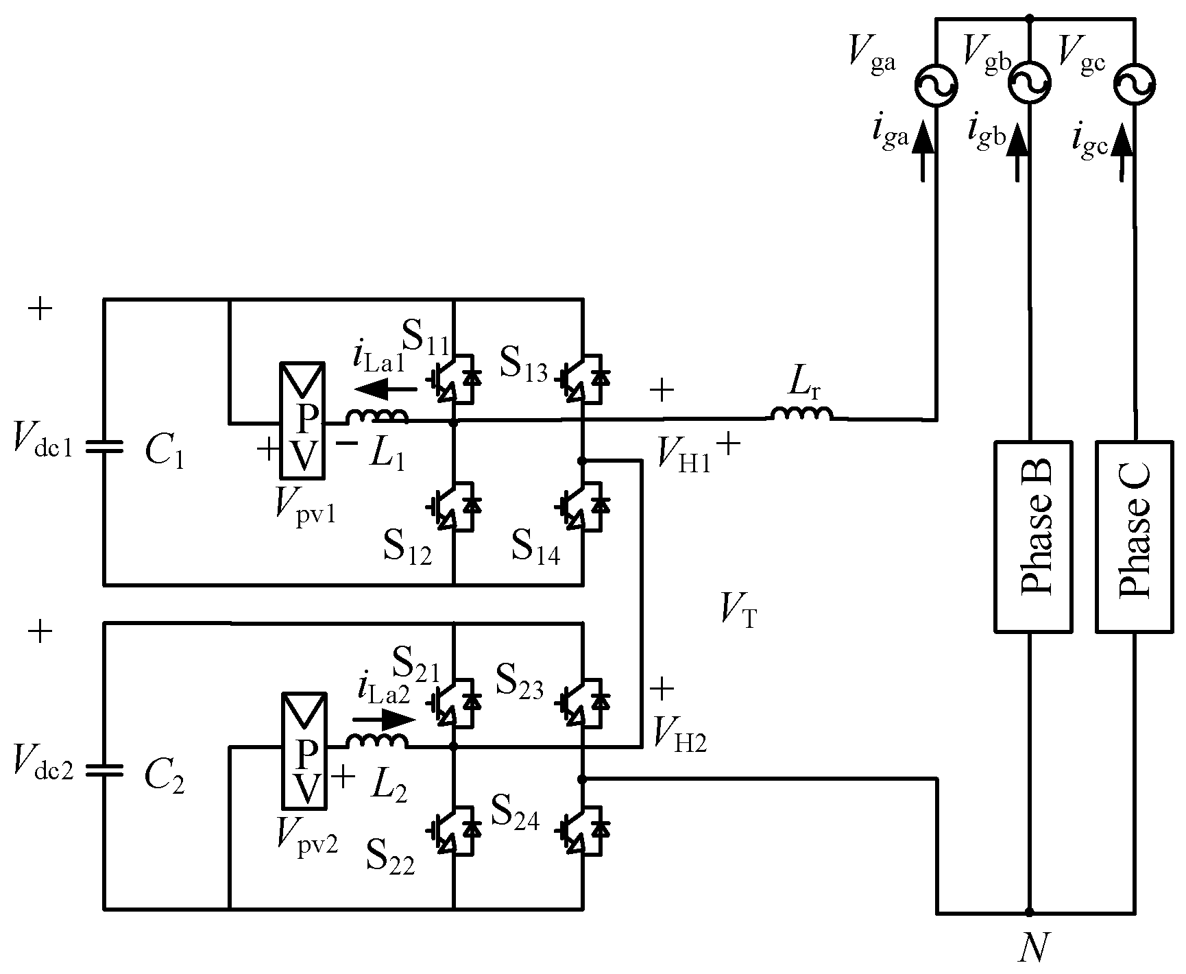
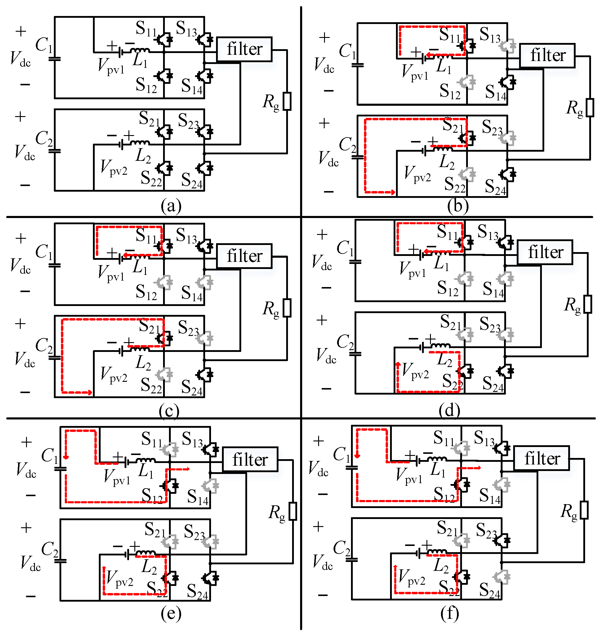
2. Topology and Operating Principle
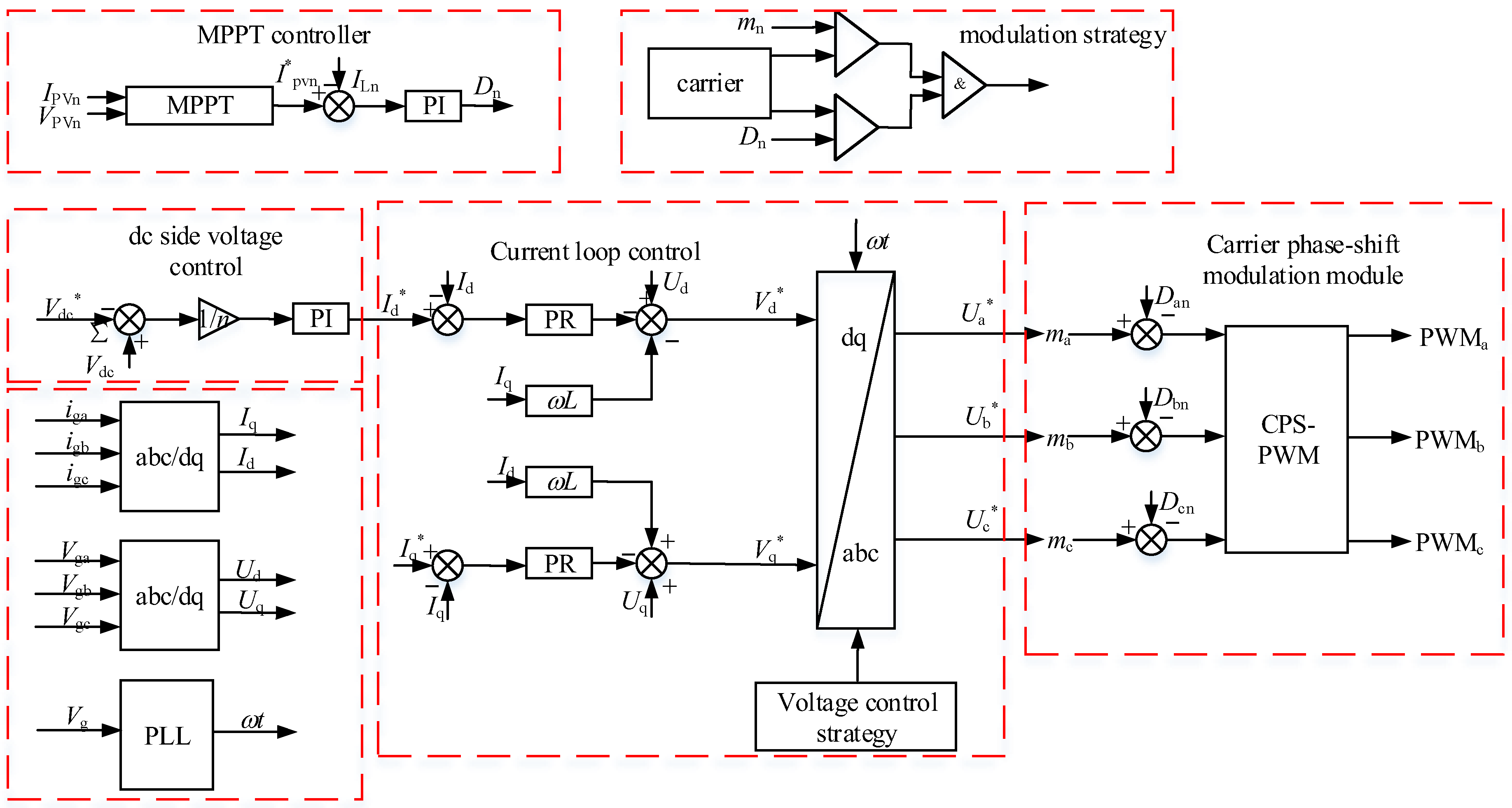
Figure 1 shows the structure of the three-phase, boost-type cascade H-bridge photovoltaic grid-connected system. Each phase of the system consists of five components: PV module, DC-side capacitor, cascaded H-bridge inverter, filter, and electrical grid. The PV module is connected to the H-bridge module, and after the energy conversion by the inverter and filtering by the filter, a grid connection is established. To ensure efficient utilization of PV modules, each PV module integrates a Maximum Power Point Tracking (MPPT) controller.
The structure illustrated in Figure 1 exemplifies the configuration of Phase A, mirroring the identical arrangements found in the remaining two phases. Compared to a two-stage photovoltaic grid-connected structure, this system eliminates the need for DC/DC modules, aiming to reduce system volume and lower costs. Subsequently, Figure 2 shows the equivalent model of the system. Vgn and ign (n = a, b, c) are marked to represent the voltage and current of the AC power grid side, while Vdc denotes the voltage across the DC-side capacitor. Vpv stands for the voltage supplied by the PV module, and iLn represents the current flowing through the inductor. VHn and VT signify the output voltage of the H-bridge and one phase of the inverter, respectively. Inductors L1 and L2, together with capacitors C1 and C2, collectively form the energy storage component, facilitating the generation of high-level output voltage.
Figure 3 shows the fundamental operation of the inverter. The inverter topology comprises eight power electronic switches, two inductors, and two capacitors, where S11–S14 constitute the upper unit and S21–S24 form the lower unit. A pair of inductors and capacitors form the impedance network.
This structure can generate up to five levels of enhanced voltage through different operational modes. Simultaneously, it can produce varying levels of output voltage by adjusting the magnitude of the modulation index (mp). The inverter exhibits five distinct operational modes. As shown in Figure 3b, when switch S11 is conducting, inductor L1 charges in a zero-state series connection with the photovoltaic power source, while the capacitor discharges to supply power to the grid, and the corresponding switch is turned on. When switch S24 is conducting, the energy stored in inductor L2 is discharged to capacitor C2 (Figure 3c). When both switches on one side of the H-bridge are conducting, the output voltage is 0 (Figure 3d). When switch S22 is conducting, inductor L2 charges in a zero-state, and the corresponding switch is turned on (Figure 3e). When switch S12 is conducting, the energy stored in inductor L1 is released to capacitor C1 (Figure 3f). Based on the above description, it can be concluded that the power electronic switches in the inverter must adopt different switching configurations when the inverter outputs different voltage levels.
Based on the equivalent model depicted in Figure 2 and the working principle of the inverter illustrated in Figure 3, the relationship between the output voltage and the input voltage of the system can be deduced. For computational convenience, the inductance on-duty ratio is set as δ and the modulation index is mp_n (n = a, b, c). The three-phase output voltage of the inverter can be expressed as:
V Ta = m p _ a V dc _ a V Tb = m p _ b V dc _ b V Tc = m p _ c V dc _ c
The expression for the modulation index mp can be obtained by Equation (1):
m p = V T V dc
According to the working principle of the circuit, the inductor is charged when the inductance on-duty ratio δ is the same as the value of the modulation index mp. Using the principle of inductor volt-second balance, the relationship between the DC-side capacitor voltage and the output voltage of the PV module can be derived as:
V dc V pv = 1 1 δ
The equation is obtained by replacing the on-duty ratio of inductor conduction in Equation (3):
V dc V PV = 1 1 m p
The relationship between the system’s output voltage and the input voltage can be obtained by simultaneously combining Equations (2) and (4) and eliminating the DC-side voltage Vdc.
V T V pv = m p 1 m p

3. Control Strategy

3.1. System-Wide Control Strategy

Figure 4 shows the control system diagram of a three-phase, boost-type CHB photovoltaic grid-connected inverter, comprising the MPPT module, DC total voltage control module, current loop control module based on the PR controller, phase-to-phase voltage control module, and carrier phase-shifted SPWM (CPS-SPWM).
The MPPT of the PV module utilizes the perturb-and-observe method. The reference current for the PV output is obtained by monitoring the voltage and current generated by the PV module. After receiving feedback from the inductor current and passing through a PI controller, it calculates the duty ratios (D1 and D2) for each PV module. These duty cycles are then utilized in subsequent modulation to achieve MPPT control. The primary responsibility of the voltage control module is to stabilize the total DC voltage of each phase and compute the input current for the current loop. The sum of all actual DC voltage values is computed, and the difference from the total specified value (Vdc*) is taken to obtain the average voltage. A PI controller ensures that the actual voltage tracks the given value while simultaneously generating the input reference signal Id* for the current loop. The reactive current component Iq* is determined according to system requirements, and typically set to 0 when the inverter operates with a specified power factor. The proportional resonant controller (PR) is adopted in the current control loop, which has the advantages of good performance and zero steady-state error control [22]. However, due to the excessive sensitivity of PR controllers to grid parameters, the adoption of a quasi-proportional resonant controller is commonly preferred. Its transfer function is:
G PR = K pc + K rc 2 ω c S S 2 + 2 ω c S + ω 0 2
To select appropriate controller parameters, a Bode plot is used to determine whether the system is stable. Firstly, the closed-loop transfer function of the system is:
G = G PR G RL 1 + ( G PR G RL )
where GRL represents the transfer function of the filter:
G RL = 1 R + S L
By substituting Equations (6) and (8) into Equation (7), the desired closed-loop transfer function can be derived. Subsequently, this function is used to generate the Bode plot illustrated in Figure 5. Figure 5 depicts the Bode plots of the current loop for three distinct parameter scenarios in the quasi-proportional resonant controller. In Case 1, both Kpc and Krc are set to 1. In Case 2, Kpc is maintained constant at 1, while Krc is increased to 5. In Case 3, Krc remains at 1, and Kpc is increased to 5. These cases are used to validate the impact of varying these parameters on the performance of the PR controller. Finally, the parameters of the PR controller are selected by example verification.
When a power imbalance occurs, the interphase control module calculates the required zero-sequence voltage. This voltage is then superimposed onto the modulated signal, resulting in the final inverter-phase modulated wave. In the modulation module, the control signal for each phase switch tube is derived by employing the carrier phase-shift modulation strategy.

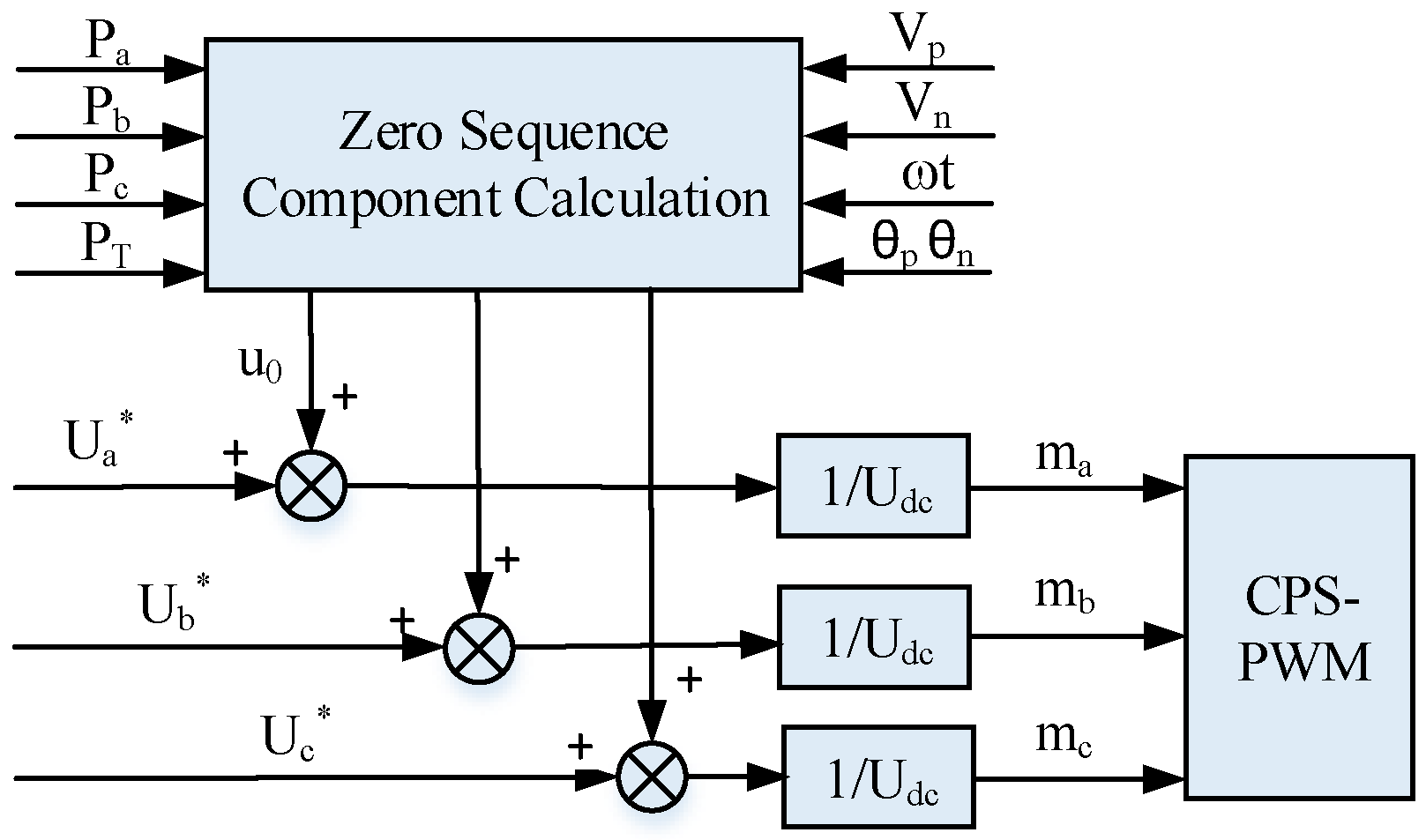
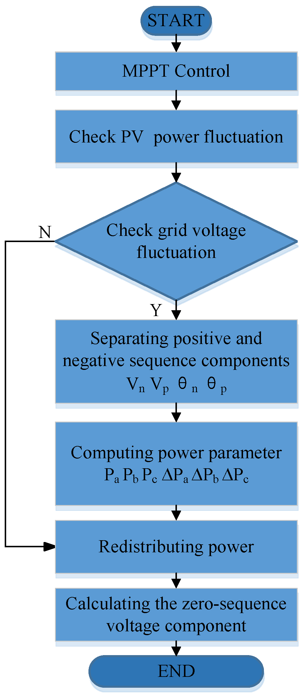
3.2. Power Imbalance Control

In practical applications, fluctuations in the input power of photovoltaic modules arise from various factors, including shading from sunlight and temperature variations. However, grid-connection requirements mandate a constant grid voltage, resulting in three-phase asymmetry in grid current [23]. Typically, the method of adding zero-sequence voltage components is adopted to address this issue. Figure 6 depicts the vector diagram that depicts the principle of compensating zero-sequence voltage components to control power balance [24,25].
As shown in Figure 6, Vgn represents the grid phase voltage of phase n (n = a, b, c), ign denotes the grid phase current of phase n, VHn* signifies the inverter output voltage before adding the zero-sequence voltage, and VHn represents the inverter output voltage after adding the zero-sequence voltage. V0 denotes the added zero-sequence component. It is evident from Figure 6 that both the amplitude and phase of the inverter output voltage undergo changes upon the addition of the zero-sequence voltage. The voltage neutral point shifts from point N to point m.
In practical scenarios, unbalanced power output from inverters may cause fluctuations at the grid connection point, leading to asymmetric currents in the grid. Under non-ideal conditions, this could potentially induce negative-sequence voltages, thereby adversely impacting the grid. This factor is taken into account in the design of the control method, and the required zero-sequence voltage is recalculated accordingly. Considering the presence of negative-sequence components, the three-phase output voltage of the inverter is recalculated, resulting in the following expression:
V Ta = V p cos ( ω t + θ p ) + V n cos ( ω t + θ n ) V Tb = V p cos ( ω t 2 π / 3 + θ p ) + V n cos ( ω t 2 π / 3 + θ n ) V Tc = V p cos ( ω t + 2 π / 3 + θ p ) + V n cos ( ω t + 2 π / 3 + θ n )
In Equation (9), Vp represents the magnitude of the positive-sequence voltage, Vn represents the magnitude of the negative-sequence voltage, ω is the grid voltage angular frequency, and θp and θn, respectively, represent the phase angles of the positive and negative-sequence voltages. When the system is required to operate at unity power factor, the negative-sequence component of the grid current is set to zero.
i g a = I cos ω t i g b = I cos ( ω t 2 π / 3 ) i g c = I cos ( ω t + 2 π / 3 )
Multiplying Equations (9) and (10), the active power output for each phase can be obtained:
P a = 0.5 V p I cos ( θ p ) + 0.5 V n I cos ( θ n ) P b = 0.5 V p I cos ( θ p ) + 0.5 V n I cos ( θ n 2 π / 3 ) P c = 0.5 V p I cos ( θ p ) + 0.5 V n I cos ( θ n + 2 π / 3 )
Three-phase total active power (PT) output of the inverter:
P T = P a + P b + P c = 1.5 V p I cos ( θ p )
Set u0 as the required zero-sequence voltage component, U0 as the voltage amplitude of the zero-sequence component, and φ as the initial phase angle of the zero-sequence voltage.
u 0 = U 0 cos ( ω t + φ )
Combined with Equations (10) and (13), the active power generated by zero-sequence voltage is obtained.
Δ P a = 0.5 U 0 I cos ( φ ) Δ P b = 0.5 U 0 I cos ( φ + 2 π / 3 ) Δ P c = 0.5 U 0 I cos ( φ 2 π / 3 )
Calculating the total active power generated by zero-sequence voltage:
Δ P a + Δ P b + Δ P c = 0
From Equation (15), it can be inferred that the superposition of zero-sequence components does not impact the total active power of the inverter; it solely redistributes the three-phase power. Pi* represents the active power output of the i-th phase after superimposing zero-sequence voltage.
P a * = P a + Δ P a P b * = P b + Δ P b P c * = P c + Δ P c
Ki indicates the degree of interphase power imbalance.
K i = P i P T ( i = a , b , c )
The power relationship must meet the following conditions:
P a * + P b * + P c * = P a + P b + P c P a * = K a P T P b * = K b P T P c * = K c P T
By substituting Equations (12), (16), and (17) into Equation (18).
Δ P a = K a P T P a = V p I cos ( θ p ) 2 P a P b P c 2 P T V n I 2 cos ( θ n )     = 2 P a P b P c 3 V n I 2 cos ( θ n ) Δ P b = K b P T P b = V p I cos ( θ p ) 2 P b P a P c 2 P T V n I 2 cos ( θ n + 2 / 3 π )     = 2 P b P a P c 3 V n I 2 cos ( θ n + 2 / 3 π ) Δ P c = K c P T P c = V p I cos ( θ p ) 2 P c P b P a 2 P T V n I 2 cos ( θ n 2 / 3 π )     = 2 P c P a P b 3 V n I 2 cos ( θ n 2 / 3 π )
Combining Equations (14) and (19):
U 0 cos φ = 2 Δ P a I = 2 P a P b P c P T V p cos ( θ p ) V n cos ( θ n ) U 0 sin φ = 2 ( Δ P b Δ P c ) 3 I = 3 ( P b P c ) P T V p cos ( θ p ) V n sin ( θ n )
Substituting Equation (20) into (13) to get the desired zero-sequence voltage:
u 0 = U 0 cos ( ω t + φ ) = U 0 cos φ cos ω t U 0 sin φ sin ω t = 2 P a P b P c P T V p cos ( θ p ) V n cos ( θ n ) cos ω t 3 ( P c P b ) P T V p cos ( θ p ) V n sin ( θ n ) sin ω t
As shown in Equation (21), this represents the final zero-sequence voltage. When the system achieves a power balance state, indicating that the three-phase output powers are equal (i.e., Pa = Pb = Pc), the value of u0 is zero, indicating that there is no need for zero-sequence voltage. In cases where the inverter’s power imbalance does not affect the grid voltage, the negative-sequence voltage component is absent. The positive-sequence voltage component Vp equals the grid voltage, and only the degree of three-phase power imbalance needs to be considered.
The block diagram of the interphase control featuring the incorporation of zero-sequence voltage is depicted in Figure 7. The system inputs encompass three-phase powers (Pa, Pb, Pc), total power (PT), positive and negative sequence voltages of the grid (Vp, Vn), phase angle (θp, θn), and the grid angular frequency. The zero-sequence voltage (u0) is derived from Equation (21) and is then incorporated into the modulation of the three-phase voltages. The resulting total signal participates in the final modulation step.
Based on the analysis conducted in the study, Figure 8 showcases the control strategy flowchart designed to tackle power balance challenges. Initially, the MPPT controller plays a pivotal role in detecting any deviations in the output power generated by the PV module. Subsequently, a comprehensive assessment of the grid’s condition ensues. In scenarios where the grid-side voltage remains stable, the system seamlessly adopts conventional power distribution and balance control measures, disregarding the positive and negative sequence components of the grid voltage. Conversely, upon detection of grid voltage fluctuations, the specialized control process outlined in Section 3.2 is promptly activated.
In general, the ability to balance system power through the zero-sequence voltage is inherently limited. Firstly, the maximum output voltage of the inverter is constrained by the voltage level at its DC side. Secondly, the requirements arising from mitigating grid voltage fluctuations impose further constraints. When the inverter’s output voltage remains within the permissible range after injecting zero-sequence components, effective balancing of grid-connected currents can be achieved. However, as the degree of three-phase power imbalance intensifies or grid-side voltage fluctuations exceed a certain threshold, the system’s output voltage may surpass its allowable upper limit, leading to overshoot. This scenario poses the potential risk of invalidating control strategies. The [26] has outlined the range of capabilities for zero-sequence voltage regulation in achieving interphase power balance. Additionally, the methodology for calculating the effective operating range of zero-sequence voltage under grid voltage fluctuations was presented in [13]. Given the above information, a more intensive analysis is conducted to examine the stability of the system under extreme conditions.

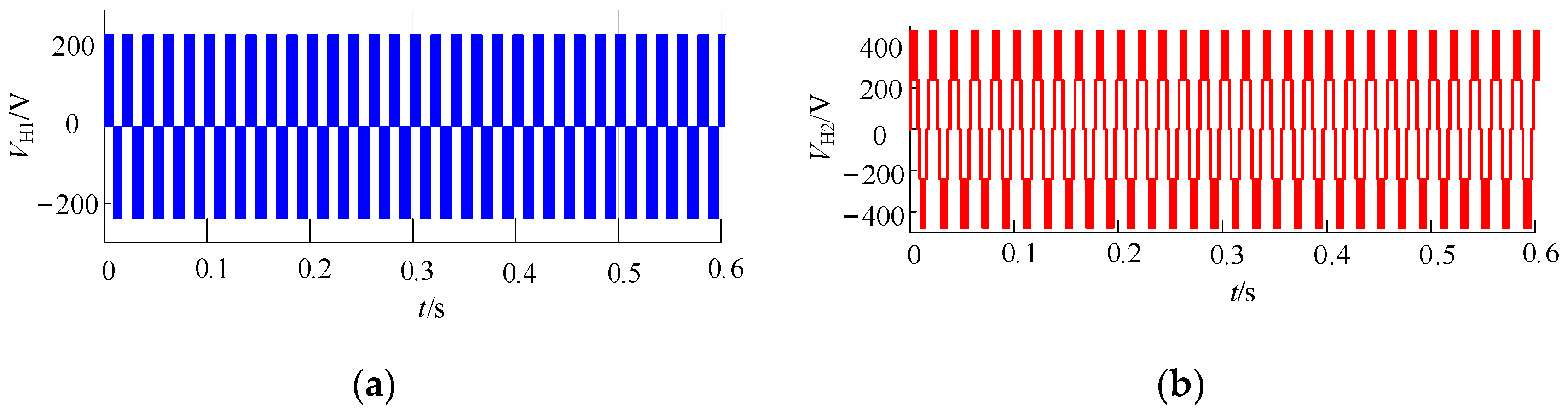
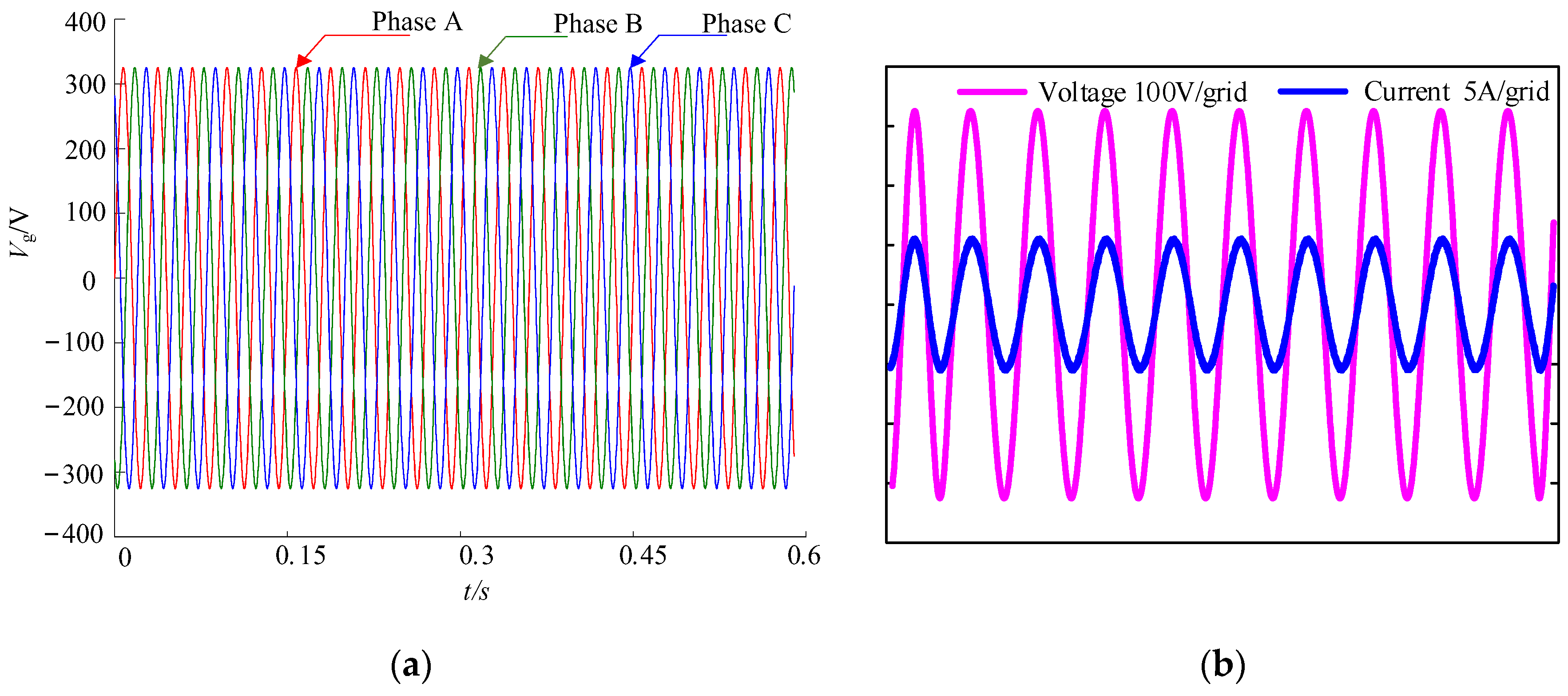
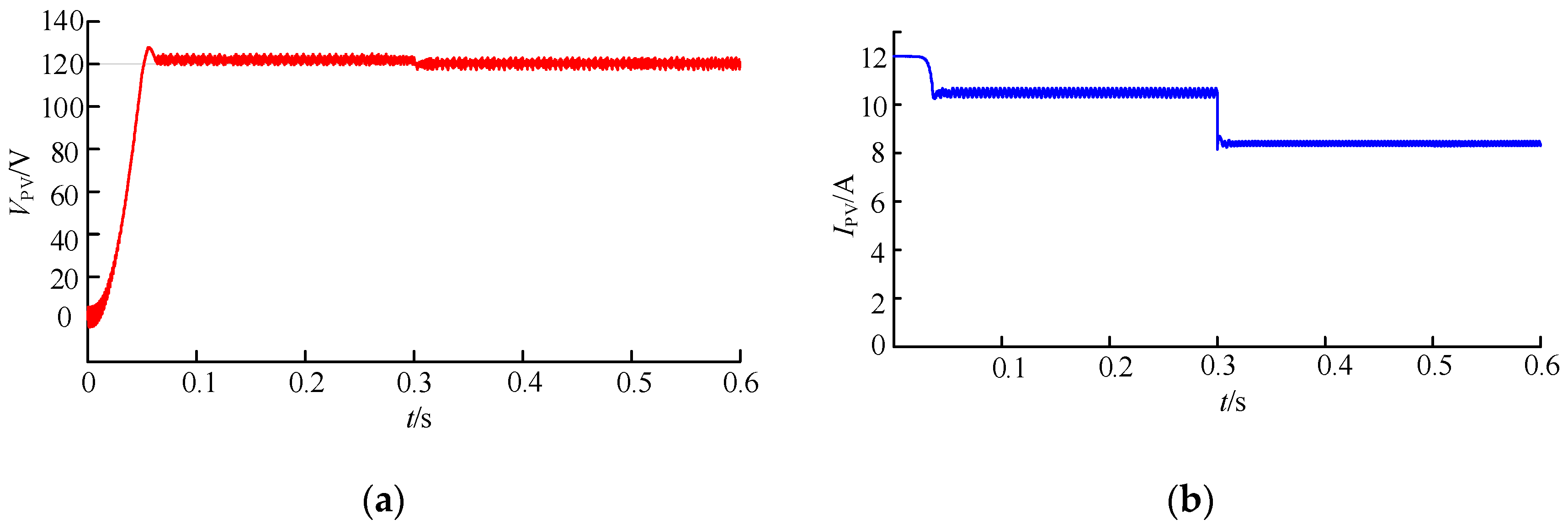
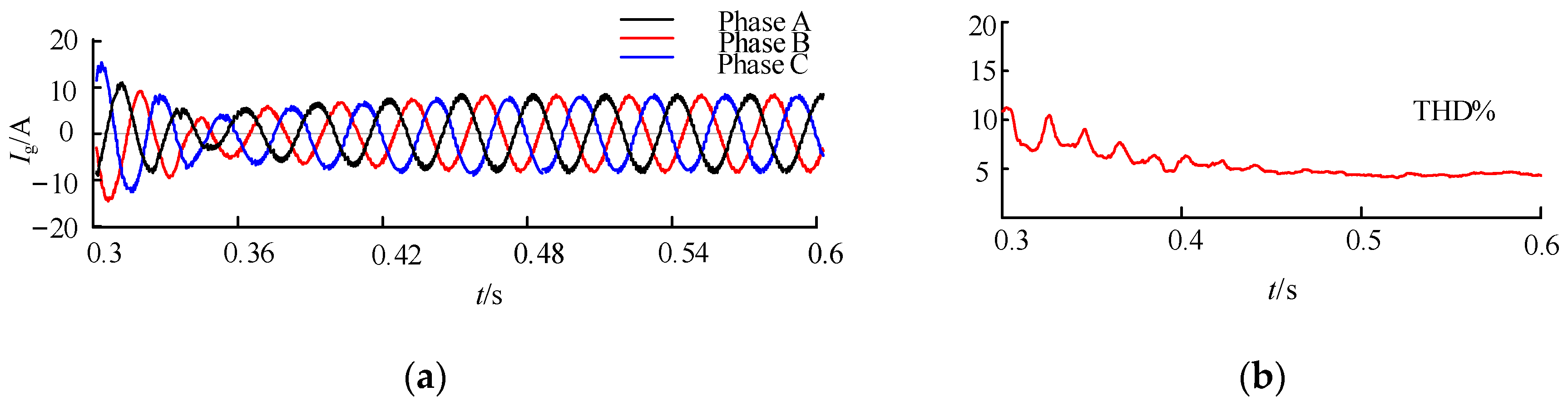
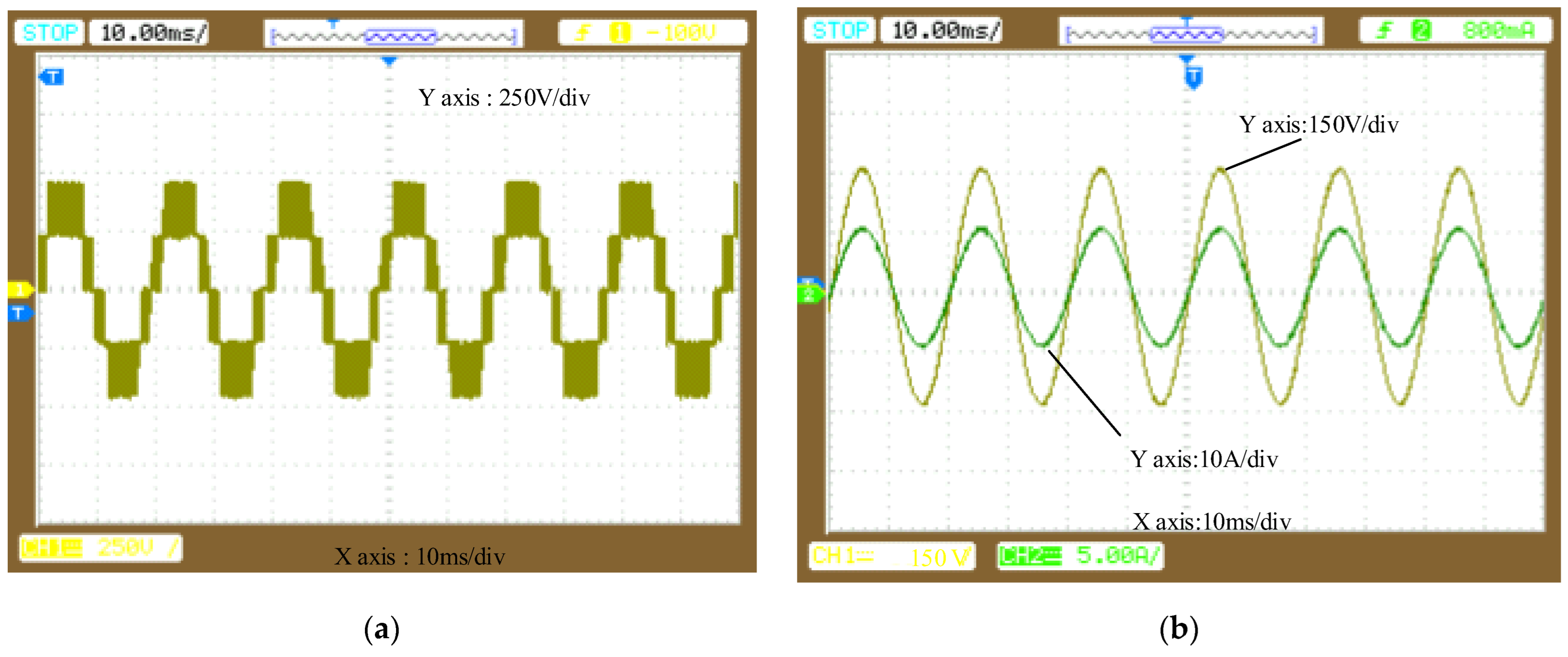
4. Simulation and Experimental Verification

In this section, the proposed system and its control strategy were validated by constructing a three-phase simulation model using Matlab R2021b/Simulink software. Table 2 presents the parameters selected for building the system.
First, the inverter’s capability to boost voltage and regulate voltage levels was validated. According to the set parameters, the input voltage of the module is 120 V. When the modulation index (mp) exceeds 0.4, the inverter produces an enhanced five-level voltage output of up to 480 V. When the modulation index mp falls below 0.3, the inverter can output three-level voltage. Figure 9 shows the output voltage of the H-bridge in steady state. Specifically, Figure 9a depicts a three-level voltage output of 240 V from one H-bridge of the inverter, achieved with a modulation index of 0.2. Figure 9b shows a five-level voltage output with a maximum voltage of 480 V from one H-bridge when the modulation index is set to 1.
To validate the performance of the photovoltaic grid-connected system, waveforms of the grid side were captured from the simulation results, as depicted in Figure 10. Figure 10a illustrates the three-phase voltage on the grid-connected side, which corresponds to the set voltage of 220 V, and the output three-phase voltage is symmetrical with an optimal waveform. Figure 10b presents the voltage and current waveform of phase A, where it is evident that the voltage and current phases are aligned, resulting in a power factor of 1.
The simulations conducted have demonstrated the system’s superior performance under standard operating conditions. Next, the performance of the system when a power imbalance occurs will be examined through simulation tests. Figure 11 illustrates the output of the PV module when the light intensity suddenly drops from 1000 to 800 at 0.3 s. Figure 11a shows the output voltage at this moment. It can be observed that the output voltage stabilizes around 120 V at 0.05 s. At 0.3 s, a decrease in irradiance causes a brief fluctuation in the PV module’s output voltage, followed by stabilization at a slightly lower amplitude. Figure 11b depicts the waveform of the output current. Initially, it stabilizes at 10.5 A around 0.05 s. However, at 0.3 s, with a drop in irradiance, there is a brief fluctuation, followed by a decrease in amplitude, ultimately stabilizing at around 8.5 A. Therefore, when the irradiance decreases at 0.3 s, the PV module still works stably at maximum power, albeit not at its maximum capacity.
To simulate voltage fluctuations in the grid, a 10% reduction in the magnitude of phase B grid voltage was introduced at 0.3 s. Figure 12 depicts the grid-connected current waveform during this change in light intensity and grid voltage. Figure 12a illustrates the waveform without the addition of power balance control. It can be observed that when the irradiance decreases at 0.3 s, due to the simultaneous reduction of the phase B grid voltage, there is a slight increase in the phase B grid current. This results in sinusoidal distortion in the overall three-phase, grid-connected current, with a notable increase in imbalance and harmonic content, thereby increasing the degree of current distortion. Figure 12b shows the waveform of grid-connected current after applying control measures. Following the introduction of these measures, the grid current experiences a brief fluctuation at 0.3 s, subsequently returning to equilibrium. At this point, the three-phase currents regain symmetry, accompanied by a slight overall decrease in their amplitudes.
To further validate the stability and robustness of the system, the system’s power imbalance was intentionally intensified, resulting in the waveform profiles presented in Figure 13. Specifically, Figure 13a illustrates the grid-side current under this condition, revealing that despite minor amplitude discrepancies, the three-phase currents remain largely symmetrical. However, waveform distortions and increase in harmonic content are present, indicating a deterioration in current quality. Figure 13b, detailing the harmonic spectrum of the currents, underscores this point by showing that at steady-state, the harmonic content has escalated to nearly 5%, approaching the tolerable threshold. In summary, although the system’s performance is slightly compromised when the power imbalance approaches its critical limit, it still retains the capability to maintain stable operation.
To further validate the proposed system and control strategy, a simulation experimental platform for a three-phase, boost-type Cascaded H-Bridge (CHB) photovoltaic grid-connected system was established. The power switch was chosen as the STP26NM60N MOSFET, and the main control chip was selected as the TMS320F28335 produced by TI. The oscilloscope model was the GDS-1102B manufactured by GWINSTEK (Xinbei, Taibei), used to indirectly observe the voltage and current waveforms generated by the system. Due to limited conditions, the photovoltaic power was replaced by power generated from the Real Time Laboratory platform. The experiment was conducted in a room temperature and safe environment, with efforts taken to minimize the impact of external factors on the experimental results.
Figure 14a shows the H-bridge output voltage during system operation, exhibiting a five-level voltage waveform with an amplitude of 480 V. Figure 14b illustrates the voltage and current waveforms of phase A, revealing a well-aligned phase between the voltage and current, consistent with the simulation results.
Due to factors such as the precision of measurement equipment, potential aging or damage of components, there may be certain impacts on the experimental results, leading to waveform distortion or shifts in amplitude and phase. Prior to the experiment, equipment should be thoroughly checked, and if circumstances permit, higher-precision and more-stable instruments should be used to conduct the experiment.
Based on the aforementioned verifications, the proposed three-phase, boost-type CHB grid-connected system has been proven to operate effectively. It successfully balances the grid waveform in scenarios of power imbalance, thereby validating the rationality of the designed structure and parameter selection.

5. Conclusions

This paper addresses the challenges of low efficiency and instability in inverters for grid-connected photovoltaic (PV) power generation systems by proposing a three-phase, boost-type cascade H-bridge PV grid-connected inverter structure, along with its power imbalance control strategy. Through a combination of theoretical calculations, simulations, and experimental validation, it is demonstrated that the proposed system exhibits remarkable performance and stability, fulfilling the following capabilities:
  • The system can enhance the input voltage by adding a minimal number of devices, thereby fulfilling the requirements of the power grid and ultimately enhancing the efficiency of the inverter.
  • When variations in the photovoltaic environment result in changes in the photovoltaic power generation, the designed control strategy enables the system to operate normally in the presence of interphase power imbalances and slight fluctuations in grid voltage.
Two primary avenues for future research endeavors have been discerned. Firstly, we will meticulously investigate, based on the current findings, the mechanism whereby intra-phase power imbalance triggers inter-phase power imbalance. Secondly, we aim to ascertain the system’s tolerable range of power unbalance and devise strategies to expand this threshold. To address these challenges, we will refine the control strategy and modulation method.
Additionally, although the proposed system exhibits strong stability, wide adaptability, and low cost, it still faces some challenges in practical applications, such as integrating with existing grid infrastructure and scaling up for large-scale deployment. After initial analysis, it is believed that the system can be extended and its operating range expanded to achieve work with existing facilities by appropriately modifying the system structure and control algorithms based on actual conditions. Furthermore, to adapt the system to different geographical and climatic conditions, adjustments to the system hardware and control strategies may be necessary to ensure stable operation in diverse environments. Extreme cold or high-temperature environments, in particular, will pose significant challenges to the system components. These issues will also become future research directions.

Author Contributions

Conceptualization, J.K. and M.Y.; methodology, J.K. and M.Y.; validation, M.Y. and B.S.; investigation, Y.X.; writing—original draft preparation, M.Y.; writing—review and editing, J.K. and M.Y.; project administration, B.L. All authors have read and agreed to the published version of the manuscript.

Funding

This research was funded by the Natural Science Foundation of Shaanxi Province, China, grant number 2023-JC-YB-381.

Data Availability Statement

The data used to support the findings of the study are available within the article.

Conflicts of Interest

The authors declare no conflicts of interest.

References

  1. Zou, C.; Xiong, B.; Xue, H.; Zheng, D.; Ge, Z.; Wang, Y.; Jiang, L.; Pan, S.; Wu, S. The role of new energy in carbon neutral. Pet. Explor. Dev. 2021, 48, 480–491. [Google Scholar] [CrossRef]
  2. Parra-Domínguez, J.; Sánchez, E.; Ordóñez, A. The Prosumer: A Systematic Review of the New Paradigm in Energy and Sustainable Development. Sustainability 2023, 15, 10552. [Google Scholar] [CrossRef]
  3. Xiang, X.; Wang, W. Economic level, environmental regulation, and new energy industry development. Environ. Sci. Pollut. Res. 2024, 31, 22814–22829. [Google Scholar] [CrossRef] [PubMed]
  4. Liu, B.; Chang, H.; Li, Y.; Zhao, Y. Analysis of influencing factors of industrial green and low-carbon transformation under the background of “double carbon”: Evidence from Sichuan province, China. Front. Environ. Sci. 2023, 11, 1257855. [Google Scholar] [CrossRef]
  5. Leon, J.I.; Kouro, S.; Franquelo, L.G.; Rodriguez, J.; Wu, B. The Essential Role and the Continuous Evolution of Modulation Techniques for Voltage-Source Inverters in the Past, Present, and Future Power Electronics. IEEE Trans. Ind. Electron. 2016, 63, 2688–2701. [Google Scholar] [CrossRef]
  6. Garnayak, R.; Kapat, S.; Chakraborty, C. Constant On/Off-Time Digital Current Control and Design Methods in Three-Level Flying-Capacitor Boost Converters for Fast Transient and Voltage Balancing. IEEE Trans. Power Electron. 2024, 39, 2980–2990. [Google Scholar] [CrossRef]
  7. Malle, L.; Mittal, A.; Kumar, S. OSG-PLL-based method of a solar PV grid-interfaced transformer-less cascaded H-bridge multilevel inverter for power quality enhancement. Electr. Eng. 2024, 1–16. [Google Scholar] [CrossRef]
  8. Goetz, S.M.; Wang, C.; Li, Z.; Murphy, D.L.K.; Peterchev, A.V. Concept of a distributed photovoltaic multilevel inverter with cascaded double H-bridge topology. Int. J. Electr. Power Energy Syst. 2019, 110, 667–678. [Google Scholar] [CrossRef]
  9. Baek, J.-Y.; Lee, K.-B. Model Predictive Current Control Strategy for Improved Dynamic Response in Cascaded H-Bridge Multilevel Inverters. J. Electr. Eng. Technol. 2024, 19, 1395–1405. [Google Scholar] [CrossRef]
  10. Wang, M.; Zhang, X.; Wu, M.; Guo, Z.; Wang, P.; Li, F. A Control Strategy for Achieving the Whole Operation Range Power Matching of Single-Phase Cascaded H-Bridge PV Inverter. IEEE Trans. Ind. Electron. 2023, 70, 5896–5906. [Google Scholar] [CrossRef]
  11. Lewicki, A.; Odeh, C.; Morawiec, M. Space Vector Pulsewidth Modulation Strategy for Multilevel Cascaded H-Bridge Inverter With DC-Link Voltage Balancing Ability. IEEE Trans. Ind. Electron. 2023, 70, 1161–1170. [Google Scholar] [CrossRef]
  12. Hua, Q.; Wang, Y.; Dong, Z.; Li, W. A Power Adaptive Control Strategy of Cascaded H-bridge Photovoltaic Inverter. Power Electron. 2022, 56, 70–73. [Google Scholar]
  13. Wang, M.; Zhang, X.; Zhao, T.; Zhuang, F.; Wang, F.; Qian, N.; Yang, S. Module Power Balance Control Strategy for Three-Phase Cascaded H-Bridge PV Inverter Under Unbalanced Grid Voltage Condition. IEEE J. Emerg. Sel. Top. Power Electron. 2021, 9, 5657–5671. [Google Scholar] [CrossRef]
  14. Tanguturi, J.; Keerthipati, S. Power Balancing Strategy for Cascaded H-Bridge Inverter in a Grid-Connected Photovoltaic System Under Asymmetrical Operating Conditions. IEEE Trans. Ind. Electron. 2024, 71, 5853–5862. [Google Scholar] [CrossRef]
  15. Liu, Y.; Ge, B.; Abu-Rub, H.; Peng, F.Z. An Effective Control Method for Quasi-Z-Source Cascade Multilevel Inverter-Based Grid-Tie Single-Phase Photovoltaic Power System. IEEE Trans. Ind. Inf. 2014, 10, 399–407. [Google Scholar] [CrossRef]
  16. Li, X.; Qin, C.; Chu, Z. Novel Space Vector Modulation Method for the Quasi-Z-Source Asymmetrical Three-Level Inverter. IEEE Trans. Circuits Syst. II Express Briefs 2024, 71, 281–285. [Google Scholar] [CrossRef]
  17. Charan, N.H.; Bandyopadhyay, A.; Guerrero, J.M. Performance Evaluation of Single-Phase Boost-Type Cascaded H-Bridge Inverter in the Applications of Grid-Tied Photovoltaic Systems. IEEE J. Emerg. Sel. Top. Power Electron. 2024, 12, 1416–1426. [Google Scholar] [CrossRef]
  18. Ge, B.; Liu, Y.; Abu-Rub, H.; Peng, F.Z. State-of-Charge Balancing Control for a Battery-Energy-Stored Quasi-Z-Source Cascaded-Multilevel-Inverter-Based Photovoltaic Power System. IEEE Trans. Ind. Electron. 2018, 65, 2268–2279. [Google Scholar] [CrossRef]
  19. Eroglu, F.; Kurtoglu, M.; Eren, A.; Vural, A.M. A novel adaptive state-of-charge balancing control scheme for cascaded H-bridge multilevel converter based battery storage systems. ISA Trans. 2023, 135, 339–354. [Google Scholar] [CrossRef] [PubMed]
  20. Sun, X.; Liu, X.; Teng, J.; Zhang, Y.; Zhao, W.; Li, X. Power balance strategy of cascaded h-bridge photovoltaic inverter based on hybrid configuration of photovoltaic and energy storage. Proc. Chin. Soc. Electr. Eng. 2024, 44, 1948–1961. [Google Scholar] [CrossRef]
  21. Qi, W.; Li, Y.; Fang, F.; Ding, L. Research on VSG grid-controlled strategy based on energy-storaged quasi-Z-source inverter. Power Syst. Prot. Control 2019, 47, 124–133. [Google Scholar]
  22. Zhen, Y.; Hou, Y.; Sha, C.; Han, B. Application of Proportional Repetitive Controller in Active Power Filter. Power Electron. 2020, 54, 99–102. [Google Scholar]
  23. Mao, W.; Zhang, X.; Zhao, T.; Hu, Y.; Wang, F.; Dai, Z.; Cao, R. Research on Power Equalization of Three-Phase Cascaded H-Bridge Photovoltaic Inverter Based on the Combination of Hybrid Modulation Strategy and Zero-Sequence Injection Methods. IEEE Trans. Ind. Electron. 2020, 67, 9337–9347. [Google Scholar] [CrossRef]
  24. Zhang, X.; Wu, M.; Wang, M.; Wang, P.; Fu, X.; Zhao, T. Review on Leakage Current Suppression and Power Balance Control of Single-phase Photovoltaic Cascaded Multilevel Inverter. Autom. Electr. Power Syst. 2023, 47, 202–215. [Google Scholar]
  25. Zhang, P.; Wu, X.; Li, B.; Ding, L.; Long, J.; Zhang, W.; Li, Y. A Zero-Sequence Component Injection PWM Scheme for Three-Level Neutral Point Clamped Rectifiers With Unbalanced DC-Link Voltages. IEEE Trans. Ind. Electron. 2024, 71, 5420–5430. [Google Scholar] [CrossRef]
  26. Yu, Y.; Konstantinou, G.; Townsend, C.D.; Agelidis, V.G. Comparison of zero-sequence injection methods in cascaded H-bridge multilevel converters for large-scale photovoltaic integration. IET Renew. Power Gener. 2017, 11, 603–613. [Google Scholar] [CrossRef]
Figure 1. Three-phase, boost-type cascade H-bridge (CHB) photovoltaic grid connected system.
Electronics 13 02819 g001
Figure 2. Equivalent model of threephase, boosttype CHB inverter.
Electronics 13 02819 g002
Figure 3. The working principle and mode of inverter: (a) The state model of the inverter; (b) the state of switching tube when the output voltage is +2Vdc; (c) the state of switching tube when the output voltage is +Vdc; (d) the state of switching tube when the output voltage is 0; (e) the state of switching tube when the voltage is −Vdc; (f) the state of switching tube when the output voltage is −2Vdc.
Electronics 13 02819 g003
Figure 4. The block diagram of control system.
Electronics 13 02819 g004
Figure 5. Bode diagrams of current loop with proportional resonant controller.
Electronics 13 02819 g005
Figure 6. Vector diagram of zero-sequence-voltage control.
Electronics 13 02819 g006
Figure 7. Diagram of zero-sequence voltage control.
Electronics 13 02819 g007
Figure 8. Flow chart of power balance control.
Electronics 13 02819 g008
Figure 9. Output voltage of H-bridge in steady state: (a) mp = 0.2; (b) mp = 1.
Electronics 13 02819 g009
Figure 10. (a) Waveforms of the grid side: grid voltage of phase A (red), grid voltage of phase B (green), grid voltage of phase C (blue); (b) voltage (pink) and current (blue) of phase A.
Electronics 13 02819 g010
Figure 11. Output of the photovoltaic module when light intensity changes: (a) voltage waveform; (b) current waveform.
Electronics 13 02819 g011
Figure 12. The waveform of grid-side current when light intensity and grid voltage change: (a) no control strategy is applied; (b) same with (a) but added control strategy.
Electronics 13 02819 g012
Figure 13. The waveform of grid-side current when power imbalance degree increases: (a) the current waveform; (b) the harmonic content of the current.
Electronics 13 02819 g013
Figure 14. (a) The experimental waveform of H-bridge output voltage; (b) the experimental waveform of A-phase voltage and current on the power grid side.
Electronics 13 02819 g014
Table 1. Comparison of one H-bridge in different boost CHB.
TypeNumber of SwitchNumber of DiodeNumber of InductorNumber of CapacitorStructureControl Strategy
Proposed topology4411SimplifiedSimplified
Quasi-Z-Source CHB4522The structure is complex and the design is difficultThe coordinated control of quasi-Z source network and CHB needs to be considered
Isolated DC–DC converter8911Many devices and isolating transformers are required; the cost is highSimplified
CHB with energy storage battery4511An additional storage battery is requiredComplex, need to consider the control of energy storage battery
Table 2. The parameter of system.
ParametersNameValue
Grid voltageUg220 V
DC side voltageUdc480 V
Frequencyfs50 Hz
Switching frequencyf10 kHz
Energy storage inductanceL11.5 mH
DC capacitanceC800 mF
Photovoltaic voltageVPV120 V
Disclaimer/Publisher’s Note: The statements, opinions and data contained in all publications are solely those of the individual author(s) and contributor(s) and not of MDPI and/or the editor(s). MDPI and/or the editor(s) disclaim responsibility for any injury to people or property resulting from any ideas, methods, instructions or products referred to in the content.

