Article

Optimal Process Design for Wake-Up Free Hf0.5Zr0.5O2 Ferroelectric Capacitors: Toward Low-Power Devices with Enhanced Ferroelectric Performance

1
China Nanhu Academy of Electronics and Information Technology, Jiaxing 314000, China
2
College of Information Science and Electronic Engineering, Zhejiang University, Hangzhou 310058, China
*
Authors to whom correspondence should be addressed.
Electronics 2024, 13(15), 2895; https://doi.org/10.3390/electronics13152895
Submission received: 24 June 2024 / Revised: 12 July 2024 / Accepted: 16 July 2024 / Published: 23 July 2024

Abstract

:
Ferroelectric hafnium and zirconium oxides have recently garnered significant attention due to their potential applications in in-memory computing. In this study, we present an optimized process design for a wake-up free 15 nm thick Hf0.5Zr0.5O2 (HZO) ferroelectric capacitor by fine-tuning the dual-oxygen process and incorporating oxygen annealing after post-metallization annealing (PMA). The optimized approach resulted in a competitive polarization of 28.6 μC/cm2, consistently exceeding 25 μC/cm2 at 3 V after 2 × 10⁷ cycles, showcasing a current density of 3.2 mA/cm2 at 2 V after 105 cycles. The synergistic effect of oxygen vacancies and grain properties (grain size, phase proportion) enables competitive ferroelectric polarization at lower voltages, while the generation of WOx near the top electrode and increased grain size further ensure the reliability of the HZO ferroelectric capacitor. This work presents innovative perspectives for the development of non-volatile devices characterized by low leakage current and low power consumption.

1. Introduction

Non-volatile memory (NVM) plays a pivotal role in facilitating energy-efficient computing, particularly in domains such as artificial intelligence and machine learning. Hafnium oxide-based ferroelectric materials emerge as promising candidates for next-generation NVM devices due to their high process compatibility, scalability, reliability, high-speed read/write capabilities, and low power consumption [1,2,3]. Among hafnium-based ferroelectric materials, zirconium-doped hafnium oxide (HZO) has witnessed rapid scientific development owing to its superior ferroelectric characteristics, lower crystallization temperature, and broader stoichiometric range [4,5]. Additionally, the fabrication of the HfO2 and ZrO2 films using the atomic layer deposition (ALD) method in complementary metal oxide semiconductor (CMOS) technology has further propelled the scientific interest in HZO [6]. Over the recent decades, various optimization methods, including element doping, oxygen vacancies, stress regulation, and interface engineering, have been explored to enhance the polarization, endurance, and reliability performance of HZO films [4,7].
Despite their favorable intrinsic material properties, HZO materials exhibit challenges such as wake-up effects and leakage current in HZO-based devices [8,9,10]. The wake-up effect in HZO films is attributed to the unpinning of ferroelectric domains and the field-induced ferroelectric phase under an applied electric field [10,11,12]. Inhibiting interface reactions through process optimization, electrode selection, and adding insulation layers has been shown to mitigate the wake-up effect [13]. However, issues such as leakage current, responsible for the degradation of ferroelectric thin films, persist. Although the leakage mechanism of ferroelectric HZO films still remains elusive, effective methods, such as adjusting the barrier height of the ferroelectric layer-electrode interface [9] and optimizing the interface defects [14,15,16], can improve film reliability. Summarizing existing reports, while the insulation layer has a positive effect on inhibiting wake-up and reducing leakage current [16], the introduced unknown interface dead layers and required large operating voltages, rendering them unstable for future low-power devices. Increasing HZO film thickness is a potential solution to suppress leakage current. However, the remanent polarization (Pr) for HZO films is significantly reduced above 10 nm, necessitating large operation voltages [8,17]. Therefore, the development of devices with low operating voltages while maintaining HZO thickness above 10 nm is crucial for achieving low-power memory devices.
In this work, we fabricated 15 nm thick HZO ferroelectric capacitors. Tungsten (W) was chosen as a capping electrode due to its superior ability to induce orthorhombic phases compared to other electrode materials [6,18,19,20], with the oxygen precursor parameters during HZO deposition having a considerable influence on HZO quality (oxygen defects) [13,21,22]. Furthermore, a synergistic optimized design using the dual-oxygen pulse recipe during HZO deposition and utilizing O2 annealing after PMA process was proposed. We selected 400 °C at 10 min as the O2 annealing condition, after fully considering the basis of the oxygen ion migration rate and HZO phase transition kinetics [23,24]. After systematically comparing the electrical characteristics and analyzing differences in HZO film structure, we demonstrated the mechanism behind enhanced ferroelectric performance. We successfully achieved larger ferroelectric polarization in 15 nm HZO films at lower operating voltages, both with wake-up free operation and improved reliability. Our work places a particular emphasis on developing low-voltage ferroelectric devices for thicker HZO films, thereby presenting a viable solution for the development of low-power memory devices.

2. Materials and Methods
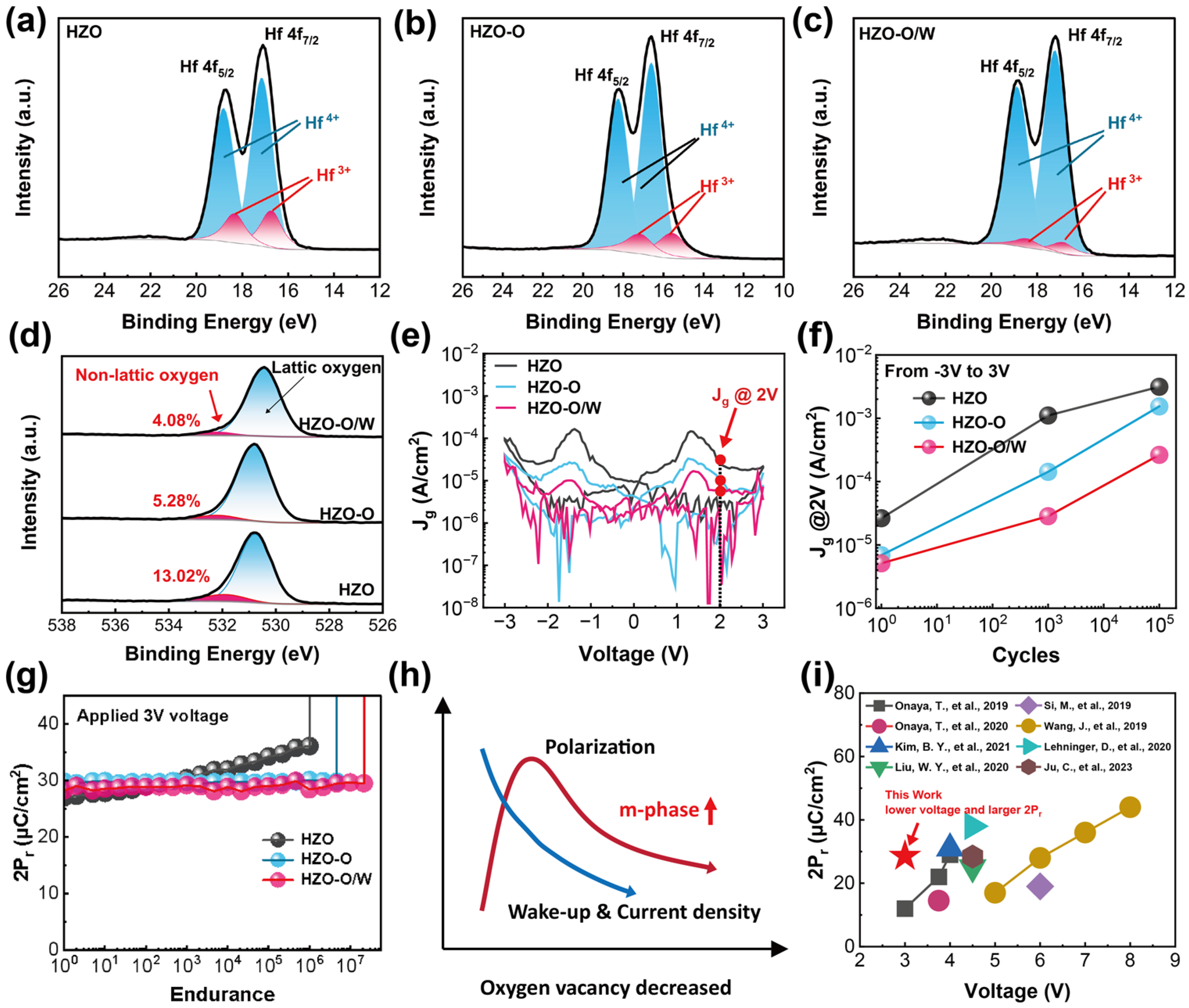
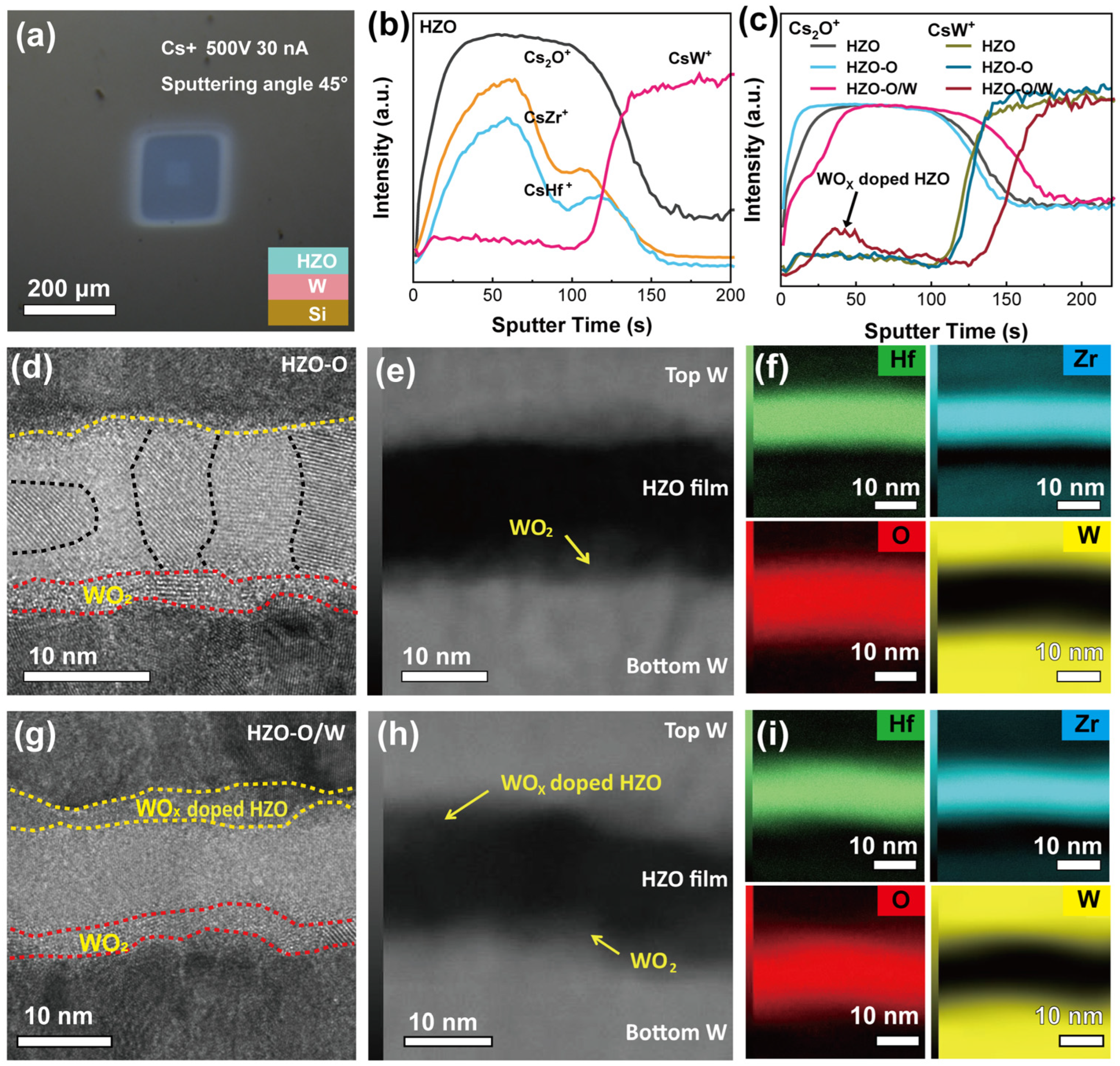
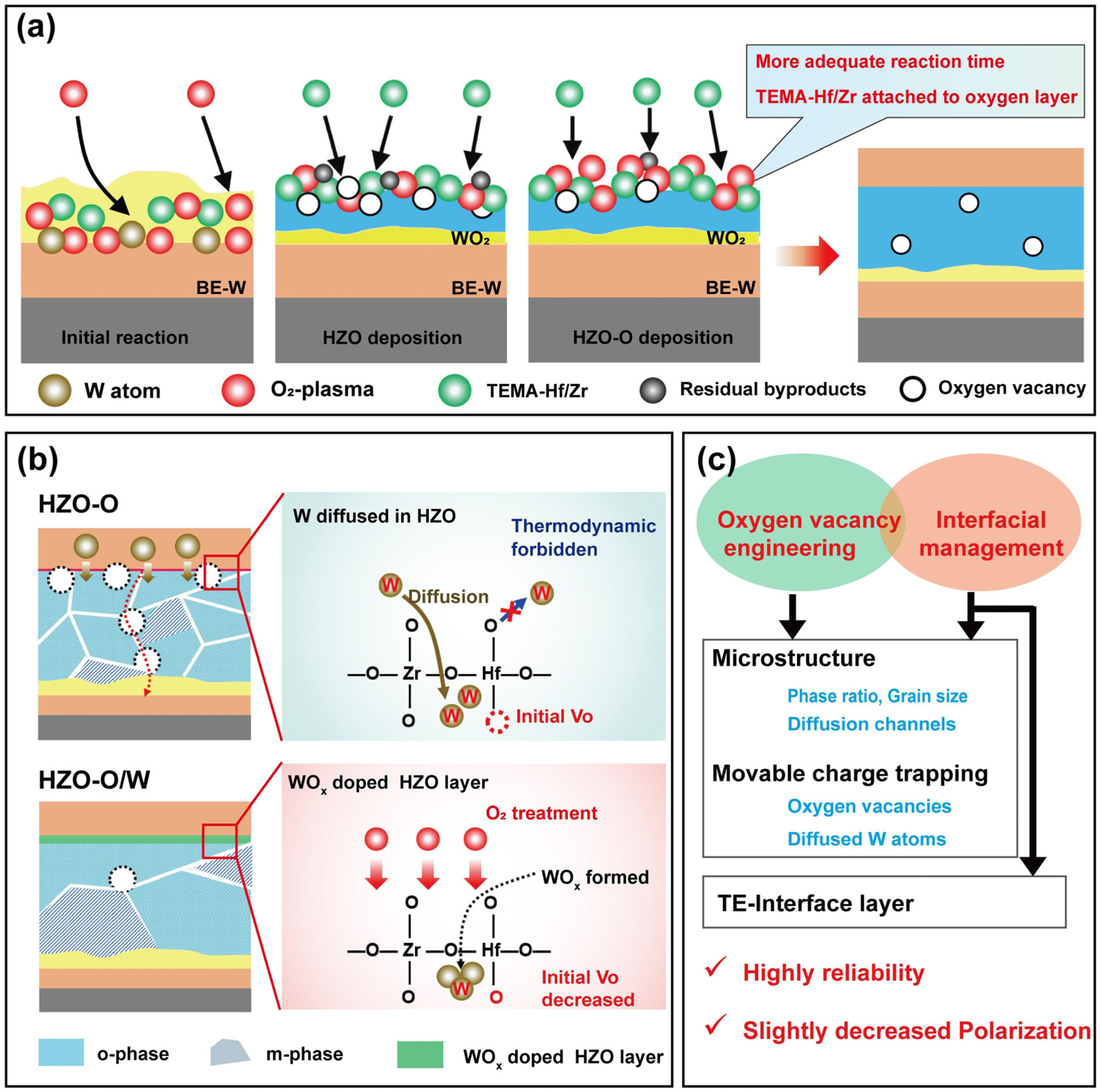
The W/HZO/W FE-capacitors were fabricated on a cleaned n-type silicon substrate by using 50 nm thick tungsten as the bottom electrode (BE), a 15 nm thick HZO as the ferroelectric dielectric, and another 50 nm thick W layer as the top electrode (TE), as shown in Figure 1a. The fabrication process involved several key steps (see Figure 1b). First, a 50 nm BE-W was deposited onto the cleaned n-type Si substrate by DC magnetron sputtering technique at room temperature. Second, plasma-enhanced atomic layer deposition (PEALD) was employed to deposit approximately 15 nm HZO films at 250 °C. Hf[N(C2H5)CH3]4, Zr[N(C2H5)CH3]4, and oxygen plasma served as the Hf precursor, Zr precursor, and oxygen source, respectively. The temperature of the Hf precursor and Zr precursor was maintained at 150 °C, and the Hf/Zr ratio was controlled by alternating deposition of one cycle HfO2 and one cycle ZrO2. Third, a 50 nm thickness TE-W was deposited, and the followed post-metallization annealing (PMA) process was performed at 500 °C for 60 s to crystallize the HZO. Finally, a 40 μm diameter circular pattern was defined on the TE-W by photolithography/etching method (marked as HZO). Meanwhile, in order to enhance the full reaction of the Hf/Zr precursor and eliminate interface defects, a dual-oxygen pulse PEALD recipe was applied during HZO deposition (marked as HZO-O). Moreover, as a further interface defects consideration, the TE-W in HZO-O was removed after PMA process, and additional processing steps, including O2 low-temperature annealing (400 °C at 10 min) and W re-deposition before TE graphical definition was performed (marked as HZO-O/W). The mass fraction with 30% H2O2 was chosen as the W etch agent in order to avoid bombardment damage caused by the traditional ICP method, and the HZO surface was adequately cleaned before W re-deposition, applying a wet cleaning recipe (Acetone → IPA → DI water).
The structural characterization of HZO films was conducted by grazing incidence X-ray diffraction (GIXRD), with Cu Kα X-ray source (λ = 1.54 Å) and an incidence angle of ∼0.5°. The micro-structure and grain properties of HZO films were estimated by high-resolution transmission electron microscopy (HRTEM) and atomic force microscopy (AFM). X-ray photoelectron spectroscopy (XPS) analysis was conducted after etching ~1 nm HZO layer by Ar plasma to eliminate potential confounding information, and considering Ar plasma could be damaging to HZO films, a moderate etching parameter (500 eV for 30 s) was employed for all devices. Time-of-flight secondary ion mass spectrometry (ToF-SIMS) was also performed to qualitatively analyses the BE interfacial information in HZO/W structures. Electrical measurements were performed by semiconductor characterization system (B1500A, Agilent Technologies, Santa Clara, CA, USA). For the polarization–voltage (P-V) measurements and endurance testing, continuous voltage pulse measurements were performed with two kinds of bipolar waveforms. The dielectric constant–voltage (εr–V) curves were acquired from small-signal capacitance measurements by applying direct current bias in addition to a tiny 30 mV AC voltage.

3. Results

The HZO TEM images showed a clear sandwich structure, as shown in Figure 1c; two clear interfaces were observed between the 15 nm thick HZO films and the W electrodes. For the EDX analysis of Hf, Zr, O, and W elements, all elements were uniformly distributed, while there existed a weak overlap in O-mapping boundaries of the bottom electrode (W) distribution region (see Figure 1d), possibly from the oxidation of BE-W. Figure 1e illustrates cross-sectional HRTEM images of the HZO device, and there clearly exists an uneven interfacial layer. Moreover, an oxide layer of approximately 1.5 nm in thickness was found at the interface between the BE-W and HZO films, which may have been generated by the reaction of reactive oxygen plasma and tungsten atoms during the initial PEALD process [25].
Furthermore, the HZO films exhibited polycrystalline structures with multiple grains, and the orthorhombic phase of HZO thin films could be identified based on diffraction spots from the marked area (red rectangle) with fast Fourier transform (FFT) images. The crystal plane spacing can be easily obtained from the inverse Fourier transform of this area, revealing the o(1 1 ¯ 1) and o(20 1 ¯ ) d-spacing of 3.03 Å and 2.65 Å, respectively [1,26]. Overall, the HZO-based capacitors show good crystallinity, and the ferroelectric orthorhombic phase is clearly formed. The observed uneven interface warrants further investigation, especially in relation to its potential impact on the device performance and stability.
Figure 2a shows the GIXRD data of 15 nm thick HZO layers with different manufacturing processes. Firstly, the diffraction peaks of W(210) and WO2(131) are cleared detected, located at 41° and 38.6°, respectively, which further evidenced the presence of tungsten oxide above the BE-W. A careful observation of the signal range (28~32°) unique to the HZO film, as shown in Figure 2b, allowed us to notice that the strength of monoclinic phase (m-phase, PDF # 04-004-3850) increased significantly after adding oxygen annealing, but it was also difficult to distinguish the signal shift of the orthorhombic (o-phase, PDF# 04-005-5597) and tetragonal (t-phase, PDF# 04-011-8820) phases [27,28]. After a further analysis of the impact of process optimization, the diffraction profiles in the GIXRD results were de-convoluted into three components for a quantitative analysis (m(11 1 ¯ ), o(111)/t(101), and m(111) diffraction peaks), and the o/t-mixture phase volume fraction was estimated as follows:
r o / t % = I o 111 / t 101 I m 11 1 ¯ + I o 111 / t 101 + I m 111 × 100
where I m 11 1 ¯ , I o 111 / t 101 , and I m 111 are the area intensities of the m(11 1 ¯ ), o(111)/t(101), and m(111) diffraction peaks, respectively.
The deconvolution results of the HZO films are summarized in Figure 2c. First, dual-oxygen pulse decreased residual organic byproducts during the HZO deposition process and further lead to more outstanding crystallization [29], showing a higher o/t-mixture phase. However, the proportion of the o/t-mixture phase decreased significantly after the HZO film was subjected to oxygen annealing, and the additional heat treatment lead to a metastable o-phase transition to a monoclinic phase, which was speculated to be related to a reduction in oxygen vacancies (VO) [29,30]. Second, the properties of HZO grains also changed with the manufacturing process. Specifically, the HZO film changed from amorphous to uniform and dense grains after PMA treatment (see Figure S1a,b). The modified PEALD process had no obvious impact on the properties of HZO grains (Figure 2d,e); however, as shown in Figure 2f, the average grain size increased from 12.3 nm to 16.7 nm after oxygen annealing, although an increase in grain size would lead to a lower surface energy effect, resulting in lower ferroelectricity. Larger grain results in there being less diffusion channels, which suppress the aggregation of defects and result in higher reliability [31].
Figure 3a illustrates the voltage loading waveform for a single P-V loop measurement and endurance cycling. Specifically, a typical positive up, negative down (PUND) method and a triangular wave with a rising/falling/delay time of 10 μs was used for P-V loop measurements, while a rectangular wave with a rise/fall time of 8 μs and a pulse duration of 4 μs was employed for endurance testing. First, Figure 3b shows P-V curves of a 15 nm HZO capacitor under various sweeping voltage conditions, revealing the strong ferroelectric nature of the HZO device, particularly when the sweeping voltage exceeds 2 V. The saturated polarization (Ps) gradually increased, reaching over 20 μC/cm2 at 5 V, and the remanent polarization (Pr, polarization-axis intercept) nearly stabilized beyond 3 V. Figure 3c showcases the P-V curve for all samples, revealing the highest 2Pr in the HZO-O device. In contrast, a slightly decreased 2Pr and a higher coercive electric field (Ec) were found in HZO-O/W. We also calculated the device-to-device consistency for all samples (see Figure S2), which showed an acceptable ±5% error in 2Pr analysis. This may be related to grain properties as well as capacitance size. The variation in 2Pr with voltage for different samples is summarized in Figure 3d. It is noteworthy that all samples achieved complete polarization under a relatively low voltage, with Pr minimally increasing beyond 3 V. In addition, a comparison between the HZO device and those prepared using a dual-oxygen pulse (HZO-O) shows an improvement in 2Pr, reaching up to 29.4 μC/cm2. Moreover, at ±3 V sweeping, the HZO-O/W exhibited a modest improvement compared to the HZO sample. The well-defined ferroelectric behavior and improvements in 2Pr in the HZO-O and HZO-O/W samples suggest the efficacy of the dual-oxygen pulse method for enhancing ferroelectric properties.
Second, the initial relative dielectric constant–voltage (εr-V) curves for all samples showed a characteristic butterfly shape (see Figure 3e), which was unique to ferroelectric materials. For the HZO sample, the dielectric constant reached a maximum value of 39.4. This value was larger than those measured on HZO-O and HZO-O/W devices, which is indicative of larger contents of the higher permittivity tetragonal phase [28]. In addition, an asymmetric peak signal was observed in HZO-O/W, which may have been caused by the m-phase grain boundary pinning action and the inconsistent thickness of the HZO/W interface layer near the top/bottom electrode, respectively [25,32]. Third, prior to P-V measurements, a 25 kHz trapezoidal wave and a 3 V amplitude were applied to the device to compare wake-up characteristics. As shown in Figure 3f, with Figure S3 showing the C-V curves and I-V curves after different cycling voltage stresses, the 2Pr of the HZO device gradually increased with the number of applied electric fields, exhibiting noticeable wake-up characteristics. In contrast, the results obtained with the HZO-O and HZO-O/W samples showed minimal change, suggesting a mitigation of the wake-up effect (see Figure 3g,h). In summary, the wake-up phenomenon of HZO is mainly caused by the electric field-induced phase transition (anti-ferroelectricity to ferroelectricity) and the redistribution of oxygen vacancies during cyclic loading electric fields [12,33]. However, the initial εr-V results rule out the contribution of an anti-ferroelectricity phase transition in this paper. By reviewing the manufacturing flow of all samples, it can be stated that oxygen vacancies may originate from an insufficient reaction in PEALD and TE-W diffusion in the PMA process, with the dual-oxygen pulse increasing the reaction’s probability of exhibiting oxygen and metal precursors. Moreover, oxygen annealing was applied on the HZO film after TE-W removal. All of this helps to eliminate oxygen vacancies. However, further research of the potential mechanisms driving wake-up free enhancements are necessary.
XPS characterization was carried out to compare the elemental composition of HZO films and verify the impact of oxygen vacancies. All devices exhibited a low carbon concentration and a nearly 1:1 elemental ratio of Hf/Zr (see Table S1). Hf 4f core-level spectrum was used for a detailed analysis of the oxygen vacancy content in all samples, as shown in Figure 4a–c. All HZO films showed double peaks at 17.1 eV and 18.8 eV, corresponding to Hf 4f7/2 and Hf 4f5/2, respectively. Moreover, Hf 4f core-level spectra revealed a presence of normal Hf4+ (18.26 eV, 16.60 eV) and incomplete oxidized Hf3+ (17.13 eV, 15.53 eV) in the HZO film [34,35]. Notably, the content of Hf3+ in the HZO film decreased with a dual-oxygen pulse application. Following the oxygen annealing process, the HZO-O/W film exhibited a minimal concentration of Hf3+. In addition, the Zr 3d core-level spectrum also showed similar trends to the Hf signals (Figure S4), indicating a further reduction in the concentration of oxygen vacancies. On the other hand, due to the O 1s of O-Hf and O-Zr being difficult to distinguish and it being difficult to quantify oxygen vacancies from the O 1s peak [27,36], the concentration of non-lattice oxygen in HZO films decreased from 13.02% to 5.28% after dual-oxygen pulse treatment and further decreased to 4.08% after the oxygen annealing process (see Figure 4d). The decrease in non-lattice oxygen also indicates a decrease in oxygen vacancies. Subsequently, the leakage current density–electric field (Jg–V) properties were also compared in this work. A bias was applied to the TE-W, transitioning from −3 V to 3 V and then back from 3 V to −3 V. As shown in Figure 4e, all devices exhibited two distinct current signals at ±1.5 V, attributed to ferroelectric domain switching. Notably, the HZO device presented more pronounced up-warping signals at −2.5 V, likely stemming from leakage current. For a direct comparison of leakage performance, the specified current density at 2 V (Jg @2V, ranging from −3 V to 3 V) of all devices was collected and is presented in Figure 4f. Obviously, the Jg increased with the number of applied bipolar stresses for all devices, and the HZO-O/W demonstrated remarkable performance, exhibiting only a 3.2 mA/cm2 leakage current density after 105 cyclic electric fields being applied, which may be due to a mechanism of stress-induced leakage currents (SILCs) [37]. SILC behavior is attributed to the redistribution of defects (such as VO). With the meticulous incorporation of dual-oxygen treatment and O2 interface annealing after the PMA process, the number of defects in HZO films was reduced and exhibited a single order of magnitude reduction in the leakage current density.
The endurance characteristics of all devices were characterized, as shown in Figure 4g. The 2Pr values exceeded 25 μC/cm2 at an applied voltage of 3V. The HZO device exhibited a gradual wake-up trend, with a breakdown occurring at ~106 cycles, consistent with the wake-up trend observed in Figure 3f. In comparison, both HZO-O and HZO-O/W devices showed improved endurance, and the HZO-O/W device achieved up to 2 × 10⁷ cycles. The effect of the oxygen vacancies and grain properties on HZO ferroelectric performance was comprehensively analyzed, as shown in Figure 4h. First, with the gradual introduction of a dual-oxygen pulse and oxygen annealing in the HZO device manufacturing process, the initial 2Pr values showed a trend of first increasing and then decreasing. Furthermore, the proportion of o-phases decreases rapidly after oxygen vacancies exceed critical values [29]. The results were also consistent with other DFT simulations and practical studies [44,45]. Second, oxygen vacancies and grain sizes also have important effects on HZO electrical reliability. The reduction in oxygen vacancies during the growth of HZO film eliminates wake-up behavior and oxygen annealing further eliminates interface defects between TE-W and HZO films. The increased grain size leads to less oxygen vacancies regarding diffusion interface channels. In summary, the HZO-O/W device shows excellent wake-up free characteristics and lower leakage current performance, emphasizing its enhanced reliability and endurance during prolonged device operations. These findings highlight the potential of dual-oxygen pulse and oxygen annealing methods in mitigating critical performance limitations in ferroelectric devices. To contextualize the polarization of 15 nm thickness HZO films, a comparison with other reported works using the same HZO thickness is presented in Figure 4i and Table S2. While the 2Pr values may not show a significant breakthrough, achieving a larger 2Pr under lower operating voltage is noteworthy.
The Top-SIMS characteristic test was performed on the HZO/W structure in order to explore the effect of optimization process on the bottom interface. The HZO/W structure formed after the PMA process was complete and removed the TE-W, and a 200 μm × 200 μm area was examined utilizing a Cs+ ion source, as depicted in Figure 5a. First, there was a gentle transition of the oxygen and W signals nearby the bottom electrode’s interface, which came from the WO2 formation during PEALD [25]. In addition, the Zr and Hf elements appeared to level off almost simultaneously, which can be understood as being caused by the matrix effect and the signal fluctuation due to the W charge effect (see Figure 5b) [46,47]. Second, the oxygen and W signals were collected to analyze the influence of the optimization process on the bottom interface, as shown in Figure 5c. The W signals had almost no shift when using the dual-oxygen pulse as the HZO layer’s growth method; however, after HZO/W was subjected to oxygen annealing treatment, a clearly rightward shift was observed for the oxygen and W signals. Moreover, the W signals were detected during initial sputtering, potentially due to the oxygen annealing that generated tungsten oxide in this area. It is speculated that the sputtering rate change at the tungsten oxide position causes the W signals to shift to the right. Figure 5d depicts the HRTEM image of the HZO-O sample, revealing a notable WO2 interface layer between HZO and BE (W), as well as depicting a simultaneous observation of grain boundaries within the HZO film. Elemental mapping analysis was further conducted for the HZO-O device, as illustrated in Figure 5e,f, demonstrating a distinct boundary between Hf and Zr near the BE-W, along with a broader oxygen distribution and narrower W depletion in the HZO region. These findings provide compelling evidence for the presence of WO2 on the bottom electrode. Figure 5g shows the HRTEM image of the HZO-O/W device, but with the WO2 layer being observed near BE-W and there being a weak amorphous region near TE-W. The structure was further analyzed via the mapping pattern and line scan profiles (see Figure 5h,i and Figure S5). It was observed that W and O distributions not only overlap near the bottom electrode but also overlap with Hf/Zr elements near the top electrode. Therefore, it is speculated that this region is a mixture of HZO and WOx [48]. To better visualize the role of the WOx layer in this work, the energy band diagrams with and without a WOx layer are shown in Figure S6. The bandgap of HZO (~5.6 eV) is higher than that of WOx (~2.7 eV), and there exists a lower barrier at the WOx/HZO interface [49]. When a negative voltage is applied, and if there is no WOx layer, the electrons from TE-W continuously flow into the HZO film. Then, they are coupled with interface traps (such as VO and holes) near the W/HZO interfaces. Meanwhile, the continuous inflow of electrons leads to the domain pinning effect, which makes it difficult for ferroelectric domains to flip. In contrast, the generation of WOx reduces the number of interface defects, thus causing the generated charge carriers to first jump over the WOx layer and then jump to the HZO film. Moreover, the WOx layer generates a partial decrease in voltage, which guarantees a lower leakage current density and higher reliability in the HZO-O/W device.
We provide mechanical insights into the improved ferroelectric performance toward low-power devices. First, during the HZO deposition process, a possibility that active O2 plasma will form an oxide layer on the bottom electrode has been reported [25], with native WO2 being beneficial in preventing BE-W diffusion to the HZO layer during the PMA process. Based on this rationale, we employ a positive approach involving dual-oxygen pulsing, and the presence of ample oxygen precursors along with sufficient reaction time facilitates a thorough removal of byproducts. Meanwhile, dual-oxygen pulses potentially form an oxygen adsorbed layer. From the viewpoint of the Hf/Zr precursor, the chemical reaction takes place on the oxygen adsorbed layer directly, rather than waiting until the next oxygen pulse (see Figure 6a). This control mechanism helps manage the total number of oxygen vacancies during HZO deposition.
Second, HZO undergoes an amorphous to ferroelectric phase transition during the PMA process. At this stage, oxygen vacancies can be divided into VO_initial and VO_crystal. To provide an approximate assessment of the oxygen vacancies, we consider the following equation:
VO_total = VO_initial + VO_crystal
where VO_initial and VO_crystal represent the oxygen vacancies in the residual amorphous and o-phases of HZO after the PMA process, respectively.
While W atoms may have a tendency to diffuse into the inside of HZO during annealing [50], the thermodynamics of metal–oxygen bonds (Hf-O ~801 kJ/mol and Zr-O ~766 kJ/mol) indicate that it is not feasible for TE-W to transform into W-O (~527 kJ/mol) by taking away oxygen atoms from a HZO structure [51,52]. At this moment, W-diffused HZOs will be formed near the TE-W, accompanied by a large number of structural defects (see Figure 6b). Under cyclic electric field loading, the presence of W atoms in the HZO structure leads to a leakage current increase as W atoms obtain and lose electrons repeatedly. Finally, in order to mitigate the adverse effects of TE-W diffusion during the PMA process, the previous TE-W layer is removed after the PMA process. Subsequently, a low-temperature O2 annealing technique is implemented prior to the deposition of a new TE-W layer. This treatment results in the conversion of diffused W atoms into amorphous WOx. Additionally, the concentration of VO_initial decreased with O2 atmosphere annealing, accompanied by an increase in grain size and variations in phase proportions. The change in grain properties leads to a slight decrease in ferroelectricity; however, the synergistic strategy of newly formed amorphous layers, fewer grain boundaries, and lower oxygen vacancies finally provide a guarantee for wake-up free, low-current-density, and high-reliability performance in HZO devices (see Figure 6c).

4. Discussion

Our findings strongly support the notion that a larger remnant polarization including wake-up free was achieved at a lower operating voltage, showcasing a lower current density via process optimization for 15 nm HZO films. A two-step process optimization was employed to eliminate the W-doped HZO layer and concurrently reduce the concentration of oxygen vacancies. This strategic approach not only ensured polarization performance but also enhanced reliability. This is particularly attractive for new non-volatile storage applications.

5. Conclusions

In this work, we successfully fabricated 15 nm thickness HZO FE-capacitors using an innovative approach that involved dual-oxygen pulsing during HZO deposition and an oxygen repair process following TE-W removal. Our optimized process resulted in a competitive 2Pr value of 28.6 μC/cm2 at a low 3 V operating voltage, surpassing the existing 15 nm HZO systems reported in the literature. The device exhibited commendable reliability, demonstrating a wake-up free behavior and minimal leakage current density during extensive loading, with 2Pr consistently exceeding 25 μC/cm2 after 2 × 10⁷ cycles and the leakage current density measuring at 3.2 mA/cm2 at 2 V after 105 cycles. Through a comprehensive analysis of grain properties, oxygen vacancies, and interfacial transformations, we identified the factors contributing to wake-up effects and decreased leakage currents. In conclusion, our work presents an alternative avenue for optimizing polarization and reliability in future low-power-consumption ferroelectric applications. The competitive 2Pr value achieved at a low operating voltage underscores the potential of our fabrication technique to advance the field of ferroelectric devices towards improved efficiency and performance.

Supplementary Materials

The following supporting information can be downloaded at: https://www.mdpi.com/article/10.3390/electronics13152895/s1. Figure S1: The 3D topography images by AFM of HZO films on the BE-W for (a) as-grown HZO, (b) PMA-treated HZO, (c) PMA-treated HZO-O and (d) PMA-treated HZO-O/W device; Figure S2: The device to device variation from 15 individual Fe-capacitors. (a) HZO, (b) HZO-O and (c) HZO-O/W. (d) The polarization distribution for statistical results; Figure S3: The I-V loops after applied different cycles trapezoid wave for (a) HZO, (b) HZO-O and (c) HZO-O/W device. The C-V loops after applied different cycles trapezoid wave for (d) HZO, (e) HZO-O and (f) HZO-O/W device; Figure S4: XPS spectra of Zr 3d core level for (a) HZO, (b) HZO-O and (C) HZO-O/W device. (d) The Zr 3d5/2 peak statistics after deconvolution; Figure S5: The TEM images (a) and line scan profiles (b) of HZO-O device. (c) TOP-SIMS depth profile of HZO-O by Cs+ ion etching. The TEM images (d) and line scan profiles (e) of HZO-O device. (f) TOP-SIMS depth profile of HZO-O/W by Cs+ ion etching; Figure S6: Schematic band diagram of the W/HZO/WO2/W stack (a) and W/WOx/HZO/WO2/W stack (b) when applied a negative voltage; Table S1: The Summary of HZO films composition and microstructure in optimization process; Table S2: The Summary of HZO films composition and microstructure in optimization process. Ref. [53] is cited in the supplementary materials.

Author Contributions

Conceptualization, H.W. and X.X.; methodology, H.W. and C.L.; software, W.W.; validation, Z.L.; formal analysis, Z.L. and W.W.; investigation, X.X.; resources, J.Q.; data curation, H.W.; writing—original draft preparation, H.W.; writing—review and editing, J.Q. and C.L.; visualization, J.Q.; supervision, C.L.; project administration, J.Q. and C.L. All authors have read and agreed to the published version of the manuscript.

Funding

This work was supported in part by the National Key Research and Development Program of China under grant 2022YFB4500102; in part by the “Pioneer” and “Leading Goose” R&D Program of Zhejiang Province under grant 2023C01018; and in part by the Shanghai Science and Technology Funding Project under grant 22DZ2205100.

Data Availability Statement

Data are contained within this article.

Acknowledgments

The authors would like to thank the ZJU-CNAEIT Joint Research and Development Center of Intelligent IoT for undertaking project management and Chenhao Zhang for providing technical support in the cleanroom.

Conflicts of Interest

The authors declare no conflicts of interest.

References

  1. Wang, Y.; Tao, L.; Guzman, R.; Luo, Q.; Zhou, W.; Yang, Y.; Wei, Y.; Liu, Y.; Jiang, P.; Chen, Y.; et al. A stable rhombohedral phase in ferroelectric Hf(Zr)1+xO2 capacitor with ultralow coercive field. Science 2023, 381, 558–563. [Google Scholar] [CrossRef] [PubMed]
  2. Peng, H.K.; Huang, Y.K.; Chou, C.P.; Wu, Y. Recognizing Spatiotemporal Features by a Neuromorphic Network with Highly Reliable Ferroelectric Capacitors on Epitaxial GeSn Film. ACS Appl. Mater. Interfaces 2021, 13, 26630–26638. [Google Scholar] [CrossRef] [PubMed]
  3. Liu, Y.; Wang, T.; Li, Z.; Yu, J.; Meng, J.; Xu, K.; Liu, P.; Zhu, H.; Sun, Q.; Zhang, D.W.; et al. Enhanced Ferroelectricity in Hf-Based Ferroelectric Device with ZrO2 Regulating Layer. Adv. Electron. Mater. 2023, 9, 2300208. [Google Scholar] [CrossRef]
  4. Kim, J.H.; Onaya, T.; Park, H.R.; Jung, Y.C.; Le, D.N.; Lee, M.; Hernandez-Arriaga, H.; Zhang, Y.; Tsai, E.H.R.; Nam, C.Y.; et al. Toward Low-Thermal-Budget Hafnia-Based Ferroelectrics via Atomic Layer Deposition. ACS Appl. Electron. Mater. 2023, 5, 4726–4745. [Google Scholar] [CrossRef]
  5. Kim, G.; Ko, D.H.; Kim, T.; Lee, S.; Jung, M.; Lee, Y.K.; Lim, S.; Jo, M.; Eom, T.; Shin, H.; et al. Power-Delay Area-Efficient Processing-In-Memory Based on Nanocrystalline Hafnia Ferroelectric Field-Effect Transistors. ACS Appl. Mater. Interfaces 2023, 15, 1463–1474. [Google Scholar] [CrossRef] [PubMed]
  6. Cui, B.; Wang, X.; Li, Y.; Wu, M.; Wu, Y.; Liu, J.; Li, X.; Ren, P.; Ye, S.; Ji, Z.; et al. Back-End-of-Line Compatible HfO2/ZrO2 Superlattice Ferroelectric Capacitor with High Endurance and Remnant Polarization. IEEE Electron Device Lett. 2023, 44, 1011–1014. [Google Scholar] [CrossRef]
  7. Yan, F.; Wu, Y.; Liu, Y.; Ai, P.; Liu, S.; Deng, S.; Xue, K.-H.; Fu, Q.; Dong, W. Recent progress on defect-engineering in ferroelectric HfO2: The next step forward via multiscale structural optimization. Mater. Horiz. 2023, 11, 626–645. [Google Scholar] [CrossRef]
  8. Lo, C.; Chang, S.C.; Lin, K.T.; Chen, C.K.; Chang, C.F.; Zhang, F.S.; Lu, Z.H.; Chao, T.S. Fabrication of Bilayer Stacked Antiferroelectric/ Ferroelectric HfxZr1-xO2 FeRAM and FeFET with Improved Leakage Current and Robust Reliability by Modifying Atomic Layer Deposition Temperatures. IEEE Electron Device Lett. 2023, 44, 883–886. [Google Scholar] [CrossRef]
  9. Cheng, X.; Zhou, C.; Lin, B.; Yang, Z.; Chen, S.; Zhang, K.H.L.; Chen, Z. Leakage mechanism in ferroelectric Hf0.5Zr0.5O2 epitaxial thin films. Appl. Mater. Today 2023, 32, 101804. [Google Scholar] [CrossRef]
  10. Saini, B.; Huang, F.; Choi, Y.Y.; Yu, Z.; Baniecki, J.D.; Thampy, V.; Tsai, W.; McIntyre, P.C. Mechanism of polarization “Wake-Up” in ferroelectric Hafnia-Zirconia thin films. Solid-State Electron. 2023, 208, 108714. [Google Scholar] [CrossRef]
  11. Saini, B.; Huang, F.; Choi, Y.Y.; Yu, Z.; Thampy, V.; Baniecki, J.D.; Tsai, W.; McIntyre, P.C. Field-Induced Ferroelectric Phase Evolution During Polarization “Wake-Up” in Hf0.5Zr0.5O2 Thin Film Capacitors. Adv. Electron. Mater. 2023, 9, 2300016. [Google Scholar] [CrossRef]
  12. Pešić, M.; Fengler, F.P.G.; Larcher, L.; Padovani, A.; Schenk, T.; Grimley, E.D.; Sang, X.; LeBeau, J.M.; Slesazeck, S.; Schroeder, U.; et al. Physical Mechanisms behind the Field-Cycling Behavior of HfO2-Based Ferroelectric Capacitors. Adv. Funct. Mater. 2016, 26, 4601–4612. [Google Scholar] [CrossRef]
  13. Kashir, A.; Oh, S.; Hwang, H. Defect Engineering to Achieve Wake-up Free HfO2-Based Ferroelectrics. Adv. Eng. Mater. 2021, 23, 2000791. [Google Scholar] [CrossRef]
  14. Xu, Y.; Yang, Y.; Zhao, S.; Gong, T.; Jiang, P.; Lv, S.; Yu, H.; Yuan, P.; Dang, Z.; Ding, Y.; et al. Robust Breakdown Reliability and Improved Endurance in Hf0.5Zr0.5O2 Ferroelectric Using Grain Boundary Interruption. IEEE Trans. Electron Devices 2022, 69, 430–433. [Google Scholar] [CrossRef]
  15. Shin, J.; Tanuma, M.; Ohmi, S. Effects of sputtering power on the formation of 5 nm thick ferroelectric nondoped HfO2 gate insulator for MFSFET application. Jpn. J. Appl. Phys. 2022, 61, SH1010. [Google Scholar] [CrossRef]
  16. Cao, Y.; Zhang, W.; Li, Y. Hafnium-doped zirconia ferroelectric thin films with excellent endurance at high polarization. Nanoscale 2023, 15, 1392–1401. [Google Scholar] [CrossRef] [PubMed]
  17. Wang, J.; Qin, M.; Zeng, M.; Gao, X.; Zhou, G.; Lu, X.; Liu, J.M.; Wang, D.; Li, Q.; Zhang, A.; et al. Excellent Ferroelectric Properties of Hf0.5Zr0.5O2 Thin Films Induced by Al2O3 Dielectric Layer. IEEE Electron Device Lett. 2019, 40, 1937–1940. [Google Scholar] [CrossRef]
  18. Yuan, P.; Wang, B.; Yang, Y.; Lv, S.; Wang, Y.; Xu, Y.; Jiang, P.; Chen, Y.; Dang, Z.; Ding, Y.; et al. Enhanced Remnant Polarization (30 μC/cm2) and Retention of Ferroelectric Hf0.5Zr0.5O2 by NH3 Plasma Treatment. IEEE Electron Device Lett. 2022, 43, 1045–1048. [Google Scholar] [CrossRef]
  19. Yang, K.; Kim, G.Y.; Ryu, J.J.; Lee, D.H.; Park, J.Y.; Kim, S.H.; Park, G.H.; Yu, G.T.; Kim, G.H.; Choi, S.Y.; et al. Wake-up-mitigated giant ferroelectricity in Hf0.5Zr0.5O2 thin films through oxygen-providing, surface-oxidized W electrode. Mater. Sci. Semicond. Process. 2023, 164, 107565. [Google Scholar] [CrossRef]
  20. Xu, P.; Yan, S.; Zhu, Y.; Zang, J.; Luo, P.; Li, G.; Yang, Q.; Chen, Z.; Zhang, W.; Zheng, X.; et al. Effects of different metal electrodes on the ferroelectric properties of HZO thin films. J. Mater. Sci. Mater. Electron. 2023, 34, 1915. [Google Scholar] [CrossRef]
  21. Kim, M.K.; Kim, I.J.; Lee, J.S. Defect Engineering of Hafnia-Based Ferroelectric Materials for High-Endurance Memory Applications. ACS Omega 2023, 8, 18180–18185. [Google Scholar] [CrossRef]
  22. Hsain, H.A.; Lee, Y.; Lancaster, S.; Materano, M.; Alcala, R.; Xu, B.; Mikolajick, T.; Schroeder, U.; Parsons, G.N.; Jones, J.L. Role of Oxygen Source on Buried Interfaces in Atomic-Layer-Deposited Ferroelectric Hafnia–Zirconia Thin Films. ACS Appl. Mater. Interfaces 2022, 14, 42232–42244. [Google Scholar] [CrossRef] [PubMed]
  23. Shvilberg, L.; Zhou, C.; Lenox, M.K.; Aronson, B.L.; Lam, N.K.; Jaszewski, S.T.; Opila, E.J.; Ihlefeld, J.F. Oxygen diffusion coefficients in ferroelectric hafnium zirconium oxide thin films. Appl. Phys. Lett. 2024, 124, 252905. [Google Scholar] [CrossRef]
  24. Park, M.H.; Chung, C.-C.; Schenk, T.; Richter, C.; Opsomer, K.; Detavernier, C.; Adelmann, C.; Jones, J.L.; Mikolajick, T.; Schroeder, U. Effect of Annealing Ferroelectric HfO2 Thin Films: In Situ, High Temperature X-Ray Diffraction. Adv. Electron. Mater. 2018, 4, 1800091. [Google Scholar] [CrossRef]
  25. Chen, H.-Y.; Jiang, Y.-S.; Chuang, C.-H.; Mo, C.-L.; Wang, T.-Y.; Lin, H.-C.; Chen, M.-J. Impact of asymmetric electrodes on ferroelectricity of sub-10 nm HZO thin films. Nanotechnology 2023, 35, 105201. [Google Scholar] [CrossRef] [PubMed]
  26. Ju, C.; Zeng, B.; Luo, Z.; Yang, Z.; Hao, P.; Liao, L.; Yang, Q.; Peng, Q.; Zheng, S.; Zhou, Y.; et al. Improved ferroelectric properties of CMOS back-end-of-line compatible Hf0.5Zr0.5O2 thin films by introducing dielectric layers. J. Mater. 2023, 24, 05013. [Google Scholar] [CrossRef]
  27. Luo, J.-D.; Lai, Y.-Y.; Hsiang, K.-Y.; Wu, C.-F.; Chung, H.-T.; Li, W.-S.; Liao, C.-Y.; Chen, P.-G.; Chen, K.-N.; Lee, M.-H.; et al. Atomic Layer Deposition Plasma-Based Undoped-HfO2 Ferroelectric FETs for Non-Volatile Memory. IEEE Electron Device Lett. 2021, 42, 1152–1155. [Google Scholar] [CrossRef]
  28. Fields, S.S.; Cai, T.; Jaszewski, S.T.; Salanova, A.; Mimura, T.; Heinrich, H.H.; Henry, M.D.; Kelley, K.P.; Sheldon, B.W.; Ihlefeld, J.F. Origin of Ferroelectric Phase Stabilization via the Clamping Effect in Ferroelectric Hafnium Zirconium Oxide Thin Films. Adv. Electron. Mater. 2022, 8, 2200601. [Google Scholar] [CrossRef]
  29. Materano, M.; Mittmann, T.; Lomenzo, P.D.; Zhou, C.; Jones, J.L.; Falkowski, M.; Kersch, A.; Mikolajick, T.; Schroeder, U. Influence of Oxygen Content on the Structure and Reliability of Ferroelectric HfxZr1–xO2 Layers. ACS Appl. Electron. Mater. 2020, 2, 3618–3626. [Google Scholar] [CrossRef]
  30. Lee, J.; Yang, K.; Kwon, J.Y.; Kim, J.E.; Han, D.I.; Lee, D.H.; Yoon, J.H.; Park, M.H. Role of oxygen vacancies in ferroelectric or resistive switching hafnium oxide. Nano Converg. 2023, 10, 55. [Google Scholar] [CrossRef]
  31. Liao, J.; Zeng, B.; Sun, Q.; Chen, Q.; Liao, M.; Qiu, C.; Zhang, Z.; Zhou, Y. Grain Size Engineering of Ferroelectric Zr-doped HfO2 for the Highly Scaled Devices Applications. IEEE Electron Device Lett. 2019, 40, 1868–1871. [Google Scholar] [CrossRef]
  32. Hiranaga, Y.; Noguchi, Y.; Mimura, T.; Shimizu, T.; Funakubo, H.; Cho, Y. Data-Driven Analysis of High-Resolution Hyperspectral Image Data Sets through Nanoscale Capacitance–Voltage Measurements to Visualize Ferroelectric Domain Dynamics. ACS Appl. Nano Mater. 2024, 7, 8525–8536. [Google Scholar] [CrossRef]
  33. Lederer, M.; Olivo, R.; Lehninger, D.; Abdulazhanov, S.; Kämpfe, T.; Kirbach, S.; Mart, C.; Seidel, K.; Eng, L.M. On the Origin of Wake-Up and Antiferroelectric-Like Behavior in Ferroelectric Hafnium Oxide. Phys. Status Solidi-Rapid Res. Lett. 2021, 15, 2100086. [Google Scholar] [CrossRef]
  34. Su, M.; Gao, S.; Weng, Z.; Zhao, L.; Lee, C.; Zhao, Y. Improvement of Ferroelectricity and Reliability in Hf0.5Zr0.5O2 Thin Films with Two-Step Oxygen Vacancy Engineering. IEEE Electron Device Lett. 2022, 43, 1057–1060. [Google Scholar] [CrossRef]
  35. Baumgarten, L.; Szyjka, T.; Mittmann, T.; Gloskovskii, A.; Schlueter, C.; Mikolajick, T.; Schroeder, U.; Müller, M. Smart Design of Fermi Level Pinning in HfO2-Based Ferroelectric Memories. Adv. Funct. Mater. 2023, 36, 2307120. [Google Scholar] [CrossRef]
  36. Kim, H.B.; Dae, K.S.; Oh, Y.; Lee, S.W.; Lee, Y.; Ahn, S.E.; Jang, J.H.; Ahn, J.H. A Simple Strategy to Realize Super Stable Ferroelectric Capacitor via Interface Engineering. Adv. Mater. Interfaces 2022, 9, 2102528. [Google Scholar] [CrossRef]
  37. Toprasertpong, K.; Takenaka, M.; Takagi, S. Breakdown-limited endurance in HZO FeFETs: Mechanism and improvement under bipolar stress. Front. Electron. 2022, 3, 1091343. [Google Scholar] [CrossRef]
  38. Onaya, T.; Nabatame, T.; Sawamoto, N.; Ohi, A.; Ikeda, N.; Nagata, T.; Ogura, A. Improvement in ferroelectricity of HfxZr1−xO2 thin films using top- and bottom-ZrO2 nucleation layers. APL Mater. 2019, 7, 061107. [Google Scholar] [CrossRef]
  39. Onaya, T.; Nabatame, T.; Inoue, M.; Jung, Y.C.; Hernandez Arriaga, H.; Mohan, J.; Kim, H.S.; Sawamoto, N.; Nagata, T.; Kim, J.; et al. Improvement in ferroelectricity and breakdown voltage of over 20-nm-thick HfxZr1−xO2/ZrO2 bilayer by atomic layer deposition. Appl. Phys. Lett. 2020, 117, 232902. [Google Scholar] [CrossRef]
  40. Kim, B.Y.; Park, H.W.; Hyun, S.D.; Lee, Y.B.; Lee, S.H.; Oh, M.; Ryoo, S.K.; Lee, I.S.; Byun, S.; Shim, D.; et al. Enhanced Ferroelectric Properties in Hf0.5Zr0.5O2 Films Using a HfO0.61N0.72 Interfacial Layer. Adv. Electron. Mater. 2021, 8, 2100042. [Google Scholar] [CrossRef]
  41. Lehninger, D.; Olivo, R.; Ali, T.; Lederer, M.; Kämpfe, T.; Mart, C.; Biedermann, K.; Kühnel, K.; Roy, L.; Kalkani, M.; et al. Back-End-of-Line Compatible Low-Temperature Furnace Anneal for Ferroelectric Hafnium Zirconium Oxide Formation. Phys. Status Solidi (A) 2020, 217, 1900840. [Google Scholar] [CrossRef]
  42. Liu, W.Y.; Liao, J.J.; Jiang, J.; Zhou, Y.C.; Chen, Q.; Mo, S.T.; Yang, Q.; Peng, Q.X.; Jiang, L.M. Highly stable performance of flexible Hf0.6Zr0.4O2 ferroelectric thin films under multi-service conditions. J. Mater. Chem. C 2020, 8, 3878–3886. [Google Scholar] [CrossRef]
  43. Si, M.; Lyu, X.; Shrestha, P.R.; Sun, X.; Wang, H.; Cheung, K.P.; Ye, P.D. Ultrafast measurements of polarization switching dynamics on ferroelectric and anti-ferroelectric hafnium zirconium oxide. Appl. Phys. Lett. 2019, 115, 072107. [Google Scholar] [CrossRef] [PubMed]
  44. Chen, J.; Xu, J.; Gong, Z.; Gu, J.; Yu, X.; Jin, C.; Peng, Y.; Liu, Y.; Chen, B.; Cheng, R.; et al. Controlling the Ferroelectricity of Doped-HfO2 via Reversible Migration of Oxygen Vacancy. IEEE Trans. Electron Devices 2023, 70, 1789–1794. [Google Scholar] [CrossRef]
  45. Islamov, D.R.; Perevalov, T.V. Effect of oxygen vacancies on the ferroelectric Hf0.5Zr0.5O2 stabilization: DFT simulation. Microelectron. Eng. 2019, 216, 111041. [Google Scholar] [CrossRef]
  46. Miwa, S.; Kusanagi, S.; Kobayashi, H. SIMS analysis of HfSiO(N) thin films. Appl. Surf. Sci. 2006, 252, 7176–7178. [Google Scholar] [CrossRef]
  47. Priebe, A.; Xie, T.; Bürki, G.; Pethö, L.; Michler, J. The matrix effect in TOF-SIMS analysis of two-element inorganic thin films. J. Anal. At. Spectrom. 2020, 35, 1156–1166. [Google Scholar] [CrossRef]
  48. Zhou, J.; Guan, Y.; Meng, M.; Hong, P.; Ning, S.; Luo, F. Improving the endurance for ferroelectric Hf0.5Zr0.5O2 thin films by interface and defect engineering. Appl. Phys. Lett. 2024, 124, 092904. [Google Scholar] [CrossRef]
  49. Zeng, B.; Xie, S.; Zhang, S.; Huang, H.; Ju, C.; Zheng, S.; Peng, Q.; Yang, Q.; Zhou, Y.; Liao, M. Polarization fatigue mechanism of laminated hafnium zirconium oxide ferroelectric thin films. Acta Mater. 2024, 272, 119920. [Google Scholar] [CrossRef]
  50. Kim, M.; Goh, Y.; Hwang, J.; Jeon, S. Enabling large ferroelectricity and excellent reliability for ultra-thin hafnia-based ferroelectrics with a W bottom electrode by inserting a metal-nitride diffusion barrier. Appl. Phys. Lett. 2021, 119, 262905. [Google Scholar] [CrossRef]
  51. Moltved, K.A.; Kepp, K.P. The Chemical Bond between Transition Metals and Oxygen: Electronegativity, d-Orbital Effects, and Oxophilicity as Descriptors of Metal–Oxygen Interactions. J. Phys. Chem. C 2019, 123, 18432–18444. [Google Scholar] [CrossRef]
  52. Mews, M.; Korte, L.; Rech, B. Oxygen vacancies in tungsten oxide and their influence on tungsten oxide/silicon heterojunction solar cells. Sol. Energy Mater. Sol. Cells 2016, 158, 77–83. [Google Scholar] [CrossRef]
  53. Lyu, X.; Si, M.; Sun, X.; Capano, M.A.; Wang, H.; Ye, P.D. Ferroelectric and Anti-Ferroelectric Hafnium Zirconium Oxide: Scaling Limit, Switching Speed and Record High Polarization Density. In Proceedings of the 2019 Symposium on VLSI Technology, Kyoto, Japan, 9–14 June 2019; pp. T44–T45. [Google Scholar]
Figure 1. (a) The MFM capacitor structure illustration. (b) Process of MFM capacitors and the preparation techniques for dual-oxygen HZO deposition (The blue dots represent the dual-oxygen HZO deposition method, and the cyan dots represent the O2 annealing process). (c) TEM image of HZO device. (d) The combination of HZO elements for corresponding EDX mapping image. (e) HRTEM images and FFT patterns of the HZO device.
Electronics 13 02895 g001
Figure 2. (a) GIXRD results of the PMA-treated HZO films on the BE-W. (b) Enlarged GIXRD results for HZO crystalline characteristics. (c) The o/t-mixture phase ratios in HZO films. The grain size statistics and AFM patterns (insert) of the PMA-treated HZO films. (d) HZO, (e) HZO-O, and (f) HZO-O/W devices.
Electronics 13 02895 g002
Figure 3. (a) The voltage waveform for P-V measurement and single endurance cycling. (b) The saturated P-V loops for HZO under different voltages. (c) The comparison of P-V loops at 3 V. (d) The variation of 2Pr with voltage. (e) The dielectric constant-voltage (εr-V) curves. The P-V loops after applied different cycles trapezoid wave for (f) HZO, (g) HZO-O, and (h) HZO-O/W devices.
Electronics 13 02895 g003
Figure 4. XPS spectra of Hf 4f core level for (a) HZO, (b) HZO-O, and (c) HZO-O/W devices. (d) XPS spectra comparison of O 1s core level. (e) Leakage current density–voltage curves. (f) The leakage current density comparison in 2V voltage after different cycles of trapezoidal waves were applied. (g) Comparison of endurance performance. (h) Effects of oxygen vacancy concentration on ferroelectric performance and reliability. (i) Comparison of 2Pr of 15 nm thick HZO with other reports [17,26,38,39,40,41,42,43].
Electronics 13 02895 g004
Figure 5. (a) Top view of the HZO device after TOP-SIMS test. (b) TOP-SIMS depth profile of HZO/W by Cs+ ion etching. (c) CsW+ and Cs2O+ depth profile with sputtering time. (d) HRTEM image of HZO-O device. (e) HZO-O morphology image. (f) Corresponding HZO-O morphology combination element mapping image. (g) HRTEM image of HZO-O/W device. (h) HZO-O/W morphology image. (i) Corresponding HZO-O/W morphology combination element mapping image.
Electronics 13 02895 g005
Figure 6. (a) The analysis of WO2 interface layer formation and oxygen vacancies variation during PEALD process. (b) Schematic illustration of W diffusion in PMA process and WOx formation in oxygen annealing. (c) Summary of the effects of structural regulation on ferroelectricity and reliability.
Electronics 13 02895 g006
Disclaimer/Publisher’s Note: The statements, opinions and data contained in all publications are solely those of the individual author(s) and contributor(s) and not of MDPI and/or the editor(s). MDPI and/or the editor(s) disclaim responsibility for any injury to people or property resulting from any ideas, methods, instructions or products referred to in the content.

