Article

Improved Design of a SiC MOSFET Gate Drive with Crosstalk Suppression Capability

College of Electrical and Power Engineering, Taiyuan University of Technology, Taiyuan 030024, China
*
Author to whom correspondence should be addressed.
Electronics 2024, 13(15), 2922; https://doi.org/10.3390/electronics13152922
Submission received: 29 June 2024 / Revised: 19 July 2024 / Accepted: 22 July 2024 / Published: 24 July 2024

Abstract

:
For high-frequency switching applications, silicon carbide (SiC) devices are more suitable than silicon-based devices, which is conducive to improving the efficiency and power density of power electronic equipment. However, as the switching frequency increases, the influence of parasitic parameters on the switching characteristics of devices becomes increasingly apparent. When SiC metal-oxide-semiconductor field-effect transistors (MOSFETs) are applied in bridge circuits, the crosstalk problem easily occurs with the complementary conduction of upper and lower transistors, which seriously limits the promotion of SiC MOSFETs. However, the existing crosstalk suppression drive circuit tends to increase the switching loss, switching delay, and control complexity; therefore, a gate drive with crosstalk suppression capability is proposed. In this paper, the gate drive has two features: a negative voltage to shut down the SiC MOSFET; and an adjustment of the gate-source equivalent impedance. To accomplish this goal, the mechanism of crosstalk voltage generation is analyzed. Furthermore, the operation principle of the gate drive is analyzed, and the parameters of the gate drive are designed. Eventually, the proposed gate drive is verified by an LTspice simulation and experimental platform. The results prove that the gate drive can suppress the crosstalk voltage without affecting the switching speed.

1. Introduction

SiC MOSFETs are wide-band gap devices that have revolutionized power electronics technology [1]. SiC MOSFETs offer the excellent characteristics of low gate charge and high speed-switching ability, which makes them more suitable for high-frequency occasions compared with Si-based devices [2]. They facilitate the improvement of the reliability, power density, and efficiency of power electronic converters and have been widely considered by the academic and industrial spheres [3,4]. However, as the switching frequency increases, dv/dt and di/dt also become larger so that parasitic parameters that are not obvious at low frequency generate voltage spikes that can damage the stability and reliability of the system [5,6,7]. In practical applications, the bridge structure is a widely used converter structure. When one switching device turns on and off, especially under the condition of a high switching speed, crosstalk voltage is generated and superimposed between the source and gate of the complementary switching device [8]. SiC MOSFETs have a lower threshold voltage compared with Si devices. Therefore, SiC MOSFETs may be turning on by mistake when the positive crosstalk voltage is generated, and even the bridge arm may pass through. This results in increased switching losses and is likely to burn out the MOSFET. In addition, because the maximum negative voltage that the SiC MOSFET gate source can withstand is very small, the negative voltage peak caused by crosstalk may exceed this value, resulting in the burning of the switching device [9,10,11]. In conclusion, when SiC MOSFETs are used in three-phase inverters, bridge DC–DC converters, and other converters with phase-leg configurations, crosstalk becomes a critical factor to evaluate, and every effort must be made to avoid false triggers and negative voltage over-ranges [12].
At present, the gate drive design for crosstalk suppression mainly includes two approaches.
One approach is to adjust the equivalent impedance between the source and the gate. In [13], crosstalk suppression is achieved by changing the drive resistance and connecting the auxiliary capacitors in parallel or series at the gate -source, but it increases the switching loss and switching delay. Crosstalk voltage can also be suppressed by adding a parallel branch composed of a MOSFET and a capacitor in series at the gate source [14]. This method has low switching losses and delays, but the MOSFET requires an extra drive signal, which can complicate control. In [15], two conduction paths (Miller capacitance and common source inductance) and three typical sources (dv/dt, di/dt, and power loop oscillation) of the crosstalk are analyzed. According to the equivalent model, a crosstalk suppression strategy of a gate parallel high-frequency diode is proposed. However, this strategy only suppresses negative crosstalk voltage. In [16], the authors proposed an improved gate drive, which suppresses the positive crosstalk voltage by actively decreasing the gate resistance and increasing the gate-source capacitance. However, the circuit is complex.
Another approach is to shut down the MOSFET by using negative voltage. In [17], the authors proposed a new RCD level shifter that suppresses crosstalk voltages below the threshold voltage by generating a negative gate voltage. However, the circuit only suppresses the positive crosstalk voltage. In the gate drive proposed in [18], a negative voltage is generated by using a voltage divider circuit and crosstalk voltage spikes are suppressed using a branch circuit consisting of a transistor series capacitor. The gate drive proposed in [8] suppresses the crosstalk voltage by changing the gate voltage and capacitor during switching transients, but the circuit adds a MOSFET, increasing the complexity of the control. In [19], suppression of crosstalk voltage is accomplished through a passive resonant level shifter consisting of a passive level shifter and a resonant tank, but this circuit increases the switching time. Moreover, crosstalk can also be suppressed by eliminating the Miller current [20], but the circuit increases the switching time.
In summary, most of the existing SiC MOSFET crosstalk suppression methods come at the expense of increasing switching losses, switching delays, or increasing control complexity. Aiming at the above problems, this paper proposes a drive circuit that has crosstalk suppression ability without increasing the switching delay. The proposed driver circuit combines negative voltage shutdown with clamp suppression and the use of resistors and capacitors to create negative voltage instead of negative voltage sources. After that, on the basis of negative pressure drive, the equivalent impedance between the gate and the source is adjusted during the switching process of the switch transistor. We analyze the designed driver circuit through a parameter design and simulation based on LTspice and finally verify it by building a synchronous buck test platform. The experimental results prove that the designed driver circuit, compared with the traditional driver circuit, can be better for crosstalk voltage positive peak attenuation below 0 V and can effectively reduce the negative crosstalk voltage while reducing the drain voltage peaks; the circuit can have a safe and stable operation.

2. Analysis of the Production Mechanism of Crosstalk Voltage

The crosstalk mechanism of the bridge circuit is shown in Figure 1. Figure 1a,b show the positive and negative crosstalk voltage generation mechanisms, respectively. The control MOSFET is represented in the circuit by M1. The synchronous MOSFET is represented in the circuit by M2. The gate internal resistance of the SiC MOSFET is represented in the circuit by Rgn(in), and Rgn(out) is the drive resistor (where n = L, H). Cdsn, Cgdn, and Cgsn are the drain-source capacitance, gate-drain capacitance, and gate-source capacitance of the SiC MOSFET (where n = L, H), respectively. Lsn(in), Lgn(in), and Ldn(in), are the parasitic inductance of the source, gate, and drain of the SiC MOSFET (where n = L, H). Lsn(out), Ldn(out), and Lgn(out) are the parasitic inductance of the source, drain, and gate line of the SiC MOSFET (where n = L, H). VDn is the body diode of the SiC MOSFET (where n = L, H). VDC is the DC power supply. L and C are the output filter inductor and capacitor. R is the load resistance. The parameters related to control MOSFET M1 are denoted by H in the subscripts. The parameters related to synchronous MOSFET M2 are denoted by L in the subscripts. In Figure 1, the control signal of S1 can control the conduction and shutdown of M1, while the control signal of S2 can control the conduction and shutdown of M2.
Before M1 was turned on, M2’s body diode VDL commutates. At the moment M1 is turning on, M1’s channel is commutated with VDL. The drain-source voltage (VdsH) of M1 drops rapidly, and the drain-source voltage (VdsL) of M2 rises rapidly. The Miller capacitor CgdL of M2 starts to charge, and the direction of the arrow is the direction of the charging current CgdLdVdsL/dt in Figure 1a. The current flows through the gate of M2 and then flows through the CgsL and the drive resistor, which raises M2’s gate-source voltage (VgsL). Moreover, the freewheeling current flowing through VDL reduces sharply, generating the crosstalk voltage on LsL (LsL = LsL(in) + LsL(out)). Together, they increase VgsL. If VgsL exceeds the threshold voltage (Vth) of M2, it will cause M2 to be turned on by mistake, causing the bridge circuit to pass through, thereby damaging M1 and M2 [21,22,23,24].
The load current flows through M1’s channel before M1 is off. When M1 is off, VDL and M1’s channel commutate. VdsH rapidly rises and VdsL rapidly declines. CgdL begins to discharge, and the discharge current is in the CgdLdVdsL/dt direction, as shown by the arrow in the Figure 1b. This current generates a left-positive and right-negative voltage drop as it flows through the gate impedance. Moreover, the negative crosstalk voltage is generated on LsL because the current starts to shift from the channel of M1 to VDL. Therefore, they work together to reduce VgsL. If the voltage peak on VgsL is more than the voltage that M2’s gate source can withstand, it is easy to cause damage to M1 and M2 [21,22,23,24].

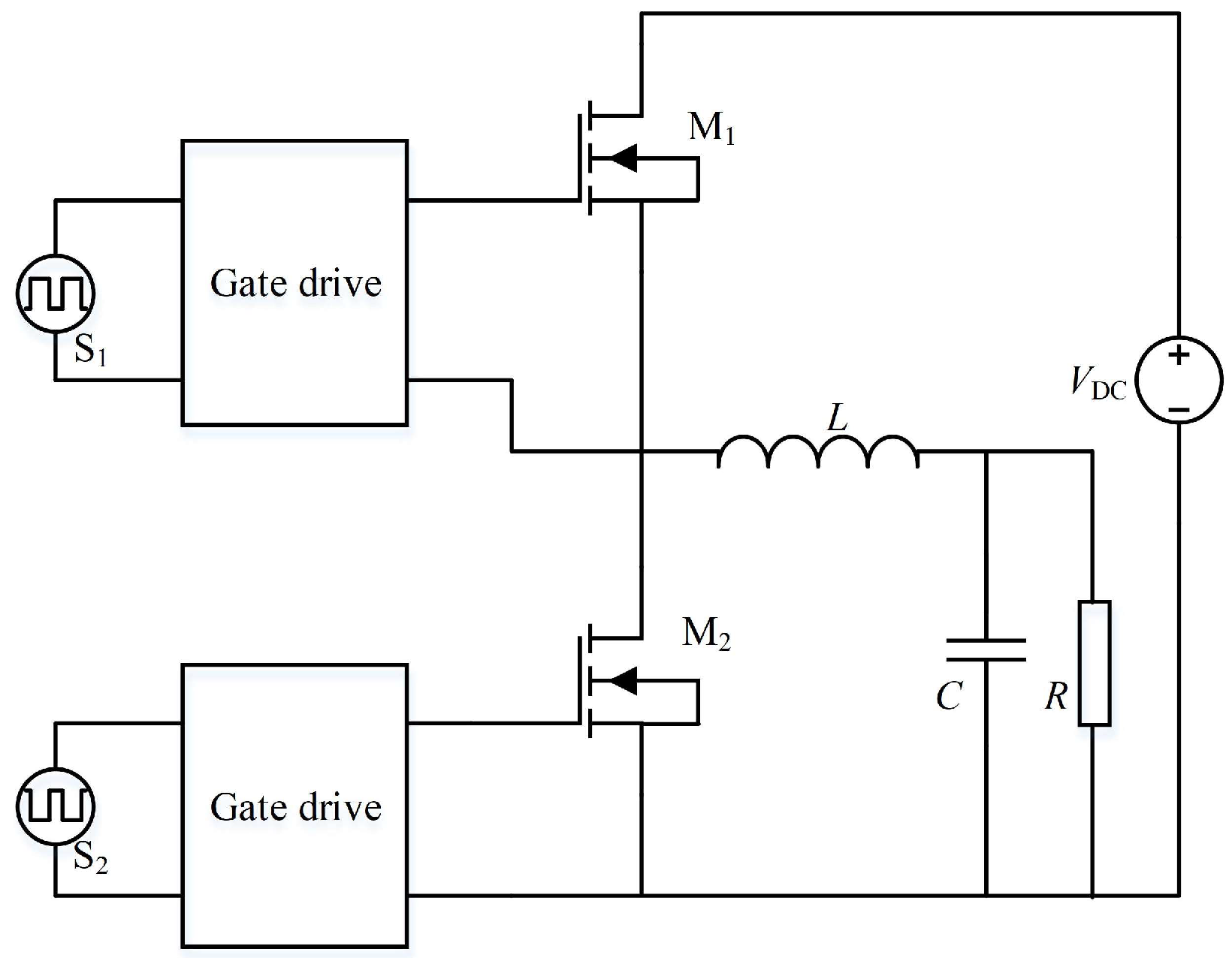
3. Operation Principle of the Improved Crosstalk Suppress Gate Drive

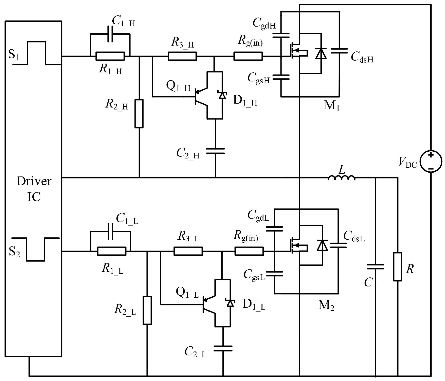
3.1. Improved Gate Drive to Suppress Crosstalk

LsL is reduced by optimizing the PCB and using the Kelvin connection to lessen the effect of LsL on crosstalk. In contrast, Miller capacitance is an inherent characteristic of SiC MOSFET [1]. The main problem in this paper is to decrease the crosstalk voltage caused by Miller capacitors. Hence, neglecting the effect of parasitic inductance, Figure 2 shows the improved gate drive for crosstalk suppression proposed in this paper. The upper transistor M1 is the control transistor, and the lower transistor M2 is the synchronous transistor.
When M1 is on, the crosstalk current flows through the driving resistor R3_L, and a voltage is generated across the R3_L. When this voltage reaches 0.7 V, the transistor Q1_L is on. At the moment, the crosstalk current flows through Q1_L and C2_L, which inhibits the forward crosstalk and reduces the impedance of the gate drive loop. After the transistor is turned on, the crosstalk displacement current is absorbed, so that when the voltage of R3_L is less than 0.7 V, Q1_L is off.
When M1 is off, M2 remains off. The capacitor C1_H provides a negative voltage for M1 to turn off M1. A crosstalk current flows through the channel formed by D1_L-C2_L when a negative crosstalk is generated. This inhibits negative crosstalk by providing a low-impedance loop for crosstalk currents.

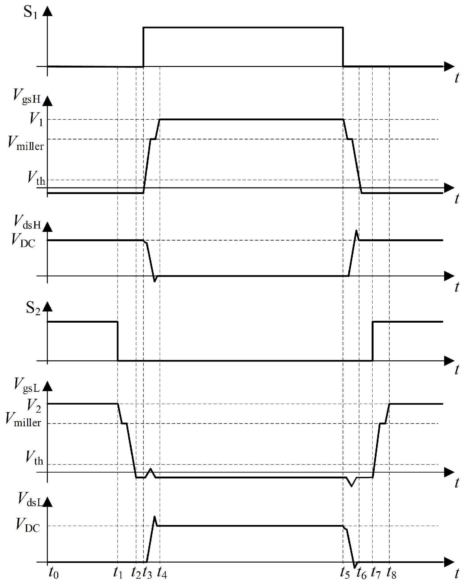
3.2. Analysis of Operation Principle of Improved Crosstalk Suppression Gate Drive

Figure 3 shows the waveform of relevant variables in a switching cycle of the improved gate drive for crosstalk suppression. S1 and S2 are the driving signals of control transistor M1 and synchronous transistor M2 in the synchronous buck circuit. The gate-source voltages of M1 and M2 are VgsH and VgsL, respectively. The drain-source voltages of M1 and M2 are VdsH and VdsL, respectively. The driving voltages of M1 and M2 are V1 and V2, respectively. The Miller voltages for M1 and M2 are Vmiller. Vth is the threshold voltage of M1 and M2.
To analyze the operation principle of the improved gate drive that suppresses crosstalk, the operation of the gate drive in a switching cycle is described in time periods, and the operation mode diagram of different time periods is shown in Figure 4, where no current flow is indicated by hidden symbols.
Mode 1[t0, t1]: The operation modal diagram of this stage is shown in Figure 4a. At this period, the control transistor M1 is completely turned off, and the synchronous transistor M2 is fully turned on. V2 charges the gate-source capacitor CgsL of M2, and the charging current flows through the divider circuit of C1_L, R1_L, R2_L to charge C1_L. The charge current flows through R3_L, and the auxiliary circuit does not work because the conduction condition of Q1_L is not met.
Mode 2[t1, t2]: The operation modal diagram of this stage is shown in Figure 4b. At t1 moment, M2 begins to turn off, and the control transistor M1 is still completely turned off. C1_L provides M2 with a negative pressure. The channel of M2 and its body diode commutate.
Mode 3[t2, t3]: The operation modal diagram of this stage is shown in Figure 4c. At this period, M1 and M2 are in the off state, and the bridge arm is in the dead zone state.
Mode 4[t3, t4]: The operation modal diagram of this stage is shown in Figure 4d. At t3 moment, M1 begins to turn on. V1 charges CgsH, and the charging current flows through the C1_H, R1_H, R2_H divider circuit to charge the capacitor C1_H. At this period, the crosstalk suppression circuit of M2 begins to work. On the one hand, the capacitor C1_L provides a negative voltage for M2 to turn off. On the other hand, M1’s channel and the M2’s body diode commutate. VdsH rapidly declines, and VdsL rapidly rises. CgdL begins to charge, and the charging current CgdLdVdsL/dt flows through R3_L to produce a right-positive and left-negative voltage drop so that Q1_L turns on. Thus, capacitor C2_L is connected to the circuit to absorb the charging current. Together, they suppress the gate-source positive crosstalk voltage of M2. After the Q1_L is turned on, the charging current is absorbed so that when the voltage across the R3_L is less than 0.7 V. Meanwhile, the Q1_L is turned off.
Mode 5[t4, t5]: The operation modal diagram of this stage is shown in Figure 4e. M1 is fully turned on and M2 is completely turned off, and the load current flows through M1’s channel.
Mode 6[t5, t6]: The operation modal diagram of this stage is shown in Figure 4f. M1 begins to turn off. At this period, M1’s channel and M2’s body diode commutate. VdsH rapidly rises, and VdsL rapidly declines. CgdL begins to discharge, and the discharge current through the C2_L-D1_L branch, reducing the equivalent impedance of the M2’s gate-source drive loop, suppressing the M2’s gate-source negative crosstalk voltage.
Mode 7[t6, t7]: The operation modal diagram of this stage is shown in Figure 4g. After the commutation is completed, the load current continues to flow through M2’s body diode. At this time, M1 and M2 are in the off state, and the bridge arm is in the dead zone state.
Mode 8[t7, t8]: The operation modal diagram of this stage is shown in Figure 4h. M2 starts to turn on, M1 remains in the off state, and M2’s channel and body diode commutate.
After the commutation, the operation mode changes to operation Mode 1, and the subsequent working mode is similar to the above process, which will not be described here.
In conclusion, the crosstalk suppression circuit proposed in this paper does not require external control signals, which reduces the complexity of the control strategy of the drive circuit and effectively suppresses the crosstalk voltage without affecting the switching speed.

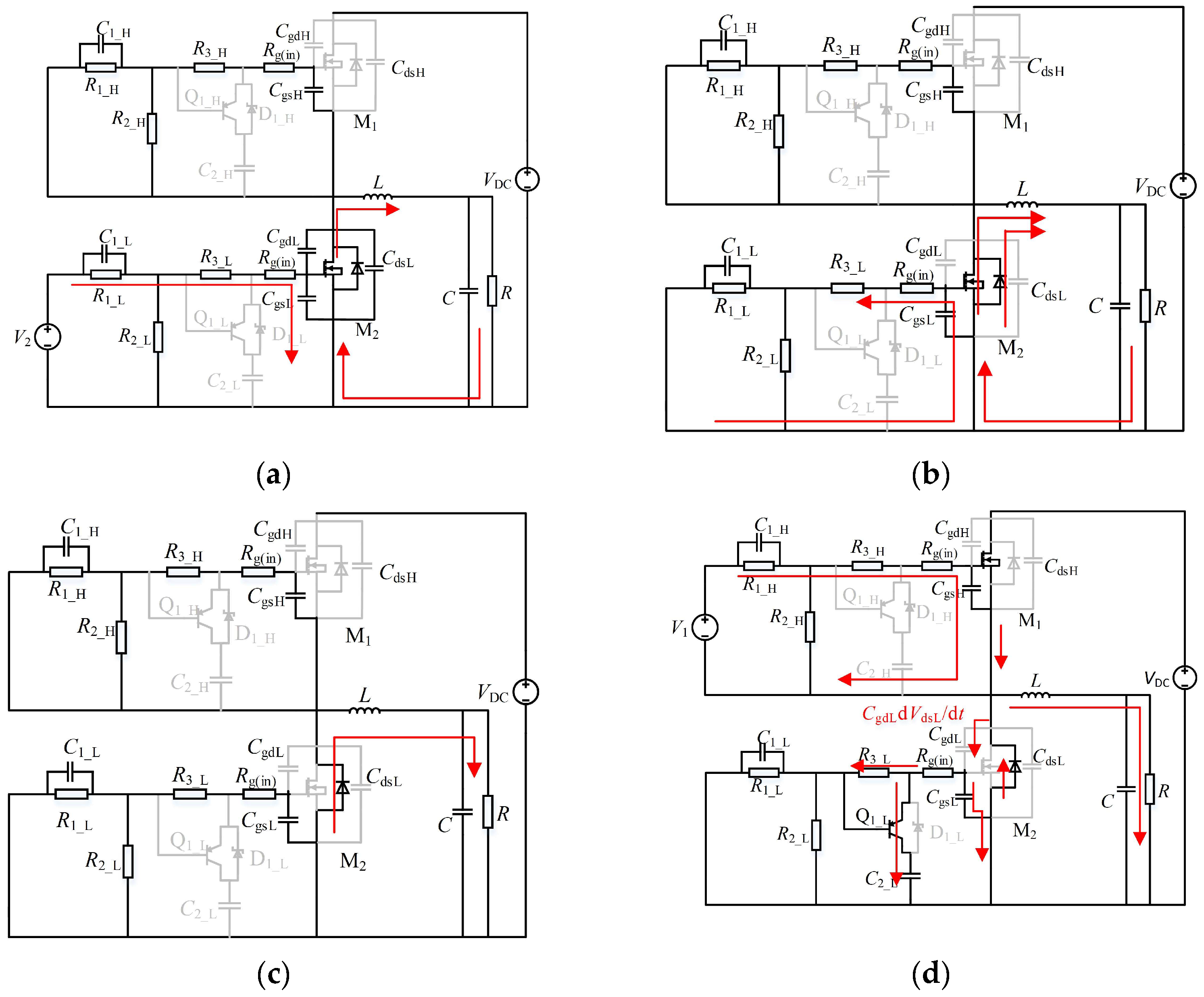
4. Parameter Design of Improved Crosstalk Suppress Gate Drive

In this paper, CREE’s second-generation 1.2 kV SiC MOSFET semiconductor device C2M0080120D is used as an example to study the parameter design of the improved gate drive, and its basic parameters are shown in Table 1. The basic parameter data in Table 1 apply to control transistor M1 and synchronous transistor M2.

4.1. Pre-Charging Process

It is essential to pre-charge C1_n to suppress crosstalk voltage before M1 and M2 enter the alternate conduction state (where n = L, H). Ensuring a constant voltage of C1_n (where n = L, H) is the purpose of the pre-charging process. The gate circuit should be pre-charged via gate voltage source V1 (V2) to ensure that capacitor C1_H (C1_L) receives sufficient energy before the main circuit starts operating. The current direction of the pre-charging process is shown in Figure 5. Both C1_n and Cgsn (where n = L, H) are charged during the pre-charging process.
The pre-charging equivalent circuits of control transistor M1 and synchronous transistor M2 are the same. Taking synchronous transistor M2 as an example, Figure 6 shows the equivalent circuit of M2’s pre-charging. According to Kirchhoff’s law and the Laplace transform, (1) is obtained:
{ R 1 _ L [ I C 1 L ( s ) I S ( s ) ] + 1 s C 1 _ L I C 1 L ( s ) = 0 R 2 _ L [ I S ( s ) I C g s L ( s ) ] R 1 _ L [ I C 1 L ( s ) I S ( s ) ] = V 2 s ( R 3 _ L + R g L ( i n ) + 1 s C g s L ) I C g s L + R 2 _ L I C g s L = R 2 _ L I S ( s )
Therefore, the current through CgsL can be expressed as:
I C g s L = V 2 A 1 s + A 2 + A 3 1 + s C 1 _ L R 1 _ L               = ( 1 A 1 s + 1 A 1 C 1 _ L R 1 _ L ) V 2 s 2 + ( 1 C 1 _ L R 1 _ L + A 2 A 1 ) s + A 2 + A 3 A 1 C 1 _ L R 1 _ L
where
A 1 = R 3 _ L + R g L ( i n ) A 2 = 1 C g s L + R 2 _ L + R 3 _ L + R g L ( i n ) R 2 _ L C 1 _ L A 3 = R 1 _ L R 2 _ L C g s L R 2 _ L + R 3 _ L + R g L ( i n ) R 2 _ L C 1 _ L
To prevent current oscillations of CgsL, C1_L and R1_L should be satisfied:
( A 1 + A 2 C 1 _ L R 1 _ L ) 2 = 4 A 1 C 1 _ L R 1 _ L ( R 1 _ L + R 2 _ L ) C g s L

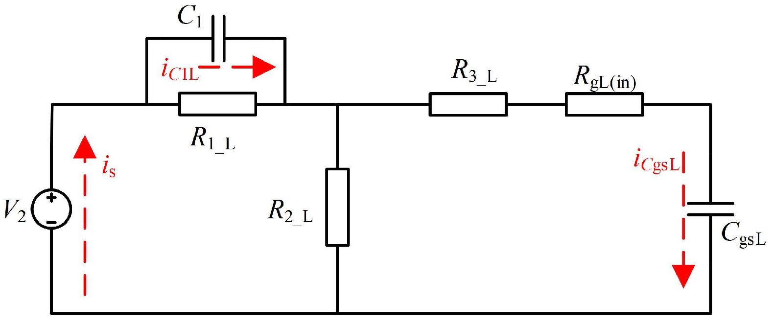
4.2. When the Auxiliary Branch Is Not Connected to the Gate Drive

When M1 is turned on and M2 remains off, the auxiliary branch is not connected to the gate drive, and the equivalent simplified circuit of the M2 drive loop is shown in Figure 7, where R = R 1 _ L × R 2 _ L R 1 _ L + R 2 _ L .
Derived from Kirchhoff’s law:
{ C g s L d V C g s L d t + I R 3 L = C g d L d V d s L d t C 1 _ L d V C 1 L d t + V C 1 L R = I R 3 L I R 3 L ( R 3 _ L + R g L ( i n ) ) + V C 1 L = V C g s L V d s L = V D C u ( t )
The expression for the crosstalk current flowing through resistor R3_L is:
I R 3 L = C g d L V D C C 1 _ L C g s L R ( R 3 _ L + R g L ( i n ) ) ×               [ e a t e b t a b + R C 1 _ L a b ( a e a t b e b t ) ]
where
a = 1 2 R C 1 _ L C g s L ( R 3 _ L + R g L ( i n ) ) × { [ C g s L ( R 3 _ L + R g L ( i n ) + R ) + R C 1 _ L ] + [ C g s L ( R 3 _ L + R g L ( i n ) + R ) + R C 1 _ L ] 2 4 R C 1 _ L C g s L ( R 3 _ L + R g L ( i n ) ) } b = 1 2 R C 1 _ L C g s L ( R 3 _ L + R g L ( i n ) ) × { [ C g s L ( R 3 _ L + R g L ( i n ) + R ) + R C 1 _ L ] [ C g s L ( R 3 _ L + R g L ( i n ) + R ) + R C 1 _ L ] 2 4 R C 1 _ L C g s L ( R 3 _ L + R g L ( i n ) ) }
After collation, the following is further obtained:
I R 3 L ( max ) = C g d L V D C C g s L ( R 3 _ L + R g L ( i n ) )
Therefore, in order to make the voltage in resistor R3_L meet the passive triggering condition of the transistor Q1_L, resistor R3_L should satisfy the following relationship [10]:
R 3 _ L > 0.7 C g s L R g L ( i n ) C g d L V D C 0.7 C g s L

4.3. When the Auxiliary Branch Is Connected to the Gate Drive

When M1 is turned on and M2 is turned off, the auxiliary branch is connected to the gate drive. The equivalent circuit is shown in Figure 8.
Equation (8) is obtained by Kirchhoff’s law:
{ I c 2 L = C 2 _ L d V C 2 L d t C d s L d V d s L d t = I I c 2 L I g V C 2 L + R g L ( i n ) I c 2 L = V C g s L I c 2 L + I g L C g d L + I g L C g s L = I I c 2 L + I g L C d s L
After collation, the expression of the voltage on capacitor C2_L is:
V C 2 L = V d c C g d L ( 1 e V d c ( C 2 _ L + C g s L + C g d L ) k R g L ( i n ) C 2 _ L ( C g s L + C g d L ) ) C 2 _ L + C g s L + C g d L
where k = dv/dt, which indicates the switching rate of M2.
Therefore, in order to ensure the effect of crosstalk suppression, the following relationship needs to be met:
{ V C 1 L + V C 2 L + 0.7 < V t h V C 1 L V C 2 L 0.4 > V max ( n e g )
In short, the basic parameters of the designed gate drive are shown in Table 2, where n = H, L.

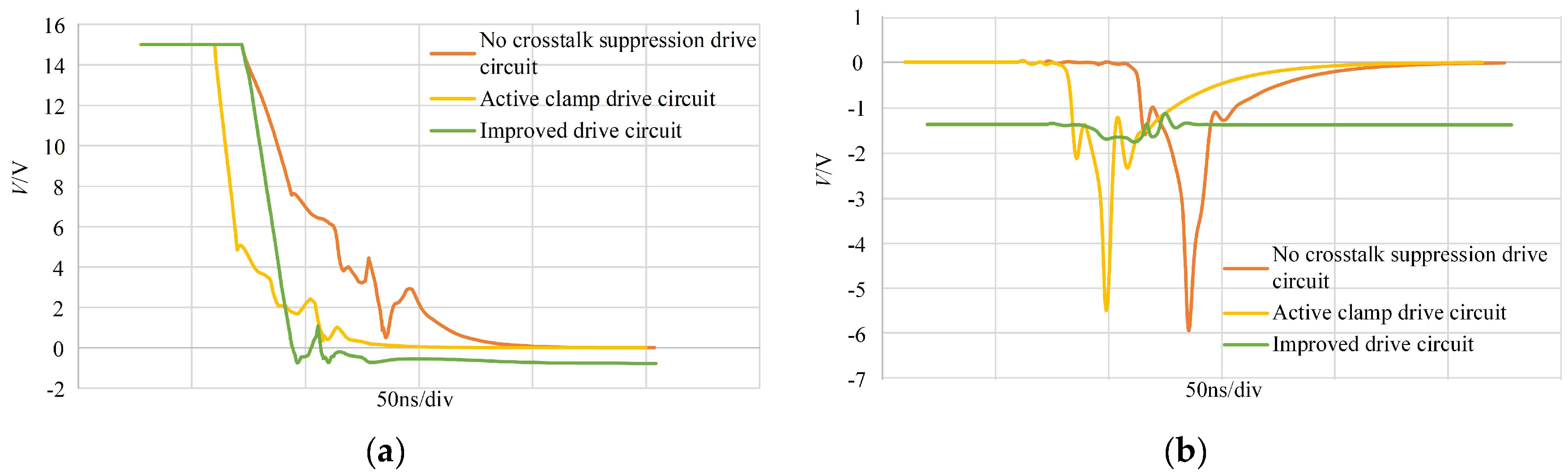
5. Simulation Verification of the Improved Crosstalk Suppression Gate Drive

The simulation of the synchronous buck circuit was based on LTspice. By changing the gate drive, the simulation results are compared and analyzed to verify the proposed gate drive. In actual circuits, the parasitic inductance is an unknown quantity, but the value of the parasitic inductance of the gate and source is usually not greater than 20 nH and has a negligible effect on power loop waveforms. In order to make the experimental conditions consistent, the value of the parasitic inductance of the gate and source is reduced by the rational design of hardware circuits when building the experimental platform, so the 2 nH inductance is added to the gate and source, respectively, to mimic the parasitic inductance in the simulation circuit.
In this study, the C2M0080120D SiC MOSFET produced by CREE was used for simulation, with a switching period of 10 μs. The selected PNP transistor was 2SAR512P, and the regulator diode was Schottky diode 1N5819. The DC side voltage of the synchronous buck circuit in the simulation was 300 V, the filtering inductance L was 500 μH, the filtering capacitance C was 470 μF, the duty cycle of the control MOSFET was 45%, and the dead time was set to 0.3 μs. The simulation models of the no-crosstalk suppression driver circuit, the active clamp drive circuit, and the improved driver circuit are shown in Figure 9, and the improved driver circuit was designed on the basis of the active clamp drive circuit.
In Figure 10, the gate-source voltages of the control switch transistor and synchronous switch transistor with a no-crosstalk suppression drive circuit, active clamp drive circuit, and improved drive circuit are compared when the upper transistor is turning on. Figure 10a shows the gate-source voltage of the control transistors, and Figure 10b shows the gate-source voltage of the synchronous transistor. When using the no-crosstalk suppression drive circuit, the positive crosstalk voltage is 4.81 V, and the negative crosstalk voltage is −4.23 V. When using the active clamp drive circuit, the positive crosstalk voltage is 2.32 V, and the negative crosstalk voltage is −5.83 V; when using the improved drive circuit, the positive crosstalk voltage is −0.05 V, and the negative crosstalk voltage is −1.47 V. As can be seen from Figure 9, active clamp circuit suppresses the positive crosstalk voltage but not the negative crosstalk voltage. The improved drive circuit can suppress both the positive and negative crosstalk voltages. In addition, the drive circuit does not disturb the switching time.
In Figure 11, when the control transistor is turned off, the gate-source voltages of the control switch transistor and synchronous switch transistor are compared in the no-crosstalk suppression drive circuit, the active clamp drive circuit, and the improved drive circuit. Figure 11a shows the gate-source voltage of the control transistors, and Figure 11b shows the gate-source voltage of the synchronous transistor. When using the no-crosstalk suppression drive circuit, the negative crosstalk voltage is −5.98 V. When using the active clamp drive circuit, the negative crosstalk voltage is −5.47 V; When using the improved drive circuit, the negative crosstalk voltage is −1.67 V. It can be concluded that the active clamp circuit suppresses the negative crosstalk voltage. The improved drive circuit can suppress the negative crosstalk voltage better. At the same time, the improved drive circuit also reduces the switching time.
Figure 12 shows the switching loss of the synchronous switch transistor, Figure 12a shows the switching loss of the synchronous transistor when the control transistor is turned on, and Figure 12b shows the switching loss of the synchronous tube when the control tube is turned off. As can be seen from Figure 12, the switching loss of the no-crosstalk suppression drive circuit is 43.67 μJ, the switching loss of the active clamp circuit is 35.14 μJ, and the switching loss of the improved drive circuit is 32.83 μJ.
In summary, the LTspice simulation results show that the crosstalk suppression gate drive designed in this paper suppresses the crosstalk voltage without sacrificing switching speed. In addition, the switching loss of the improved drive circuit is almost the same or even slightly reduced compared with the no-crosstalk suppression drive circuit and the active clamp drive circuit.

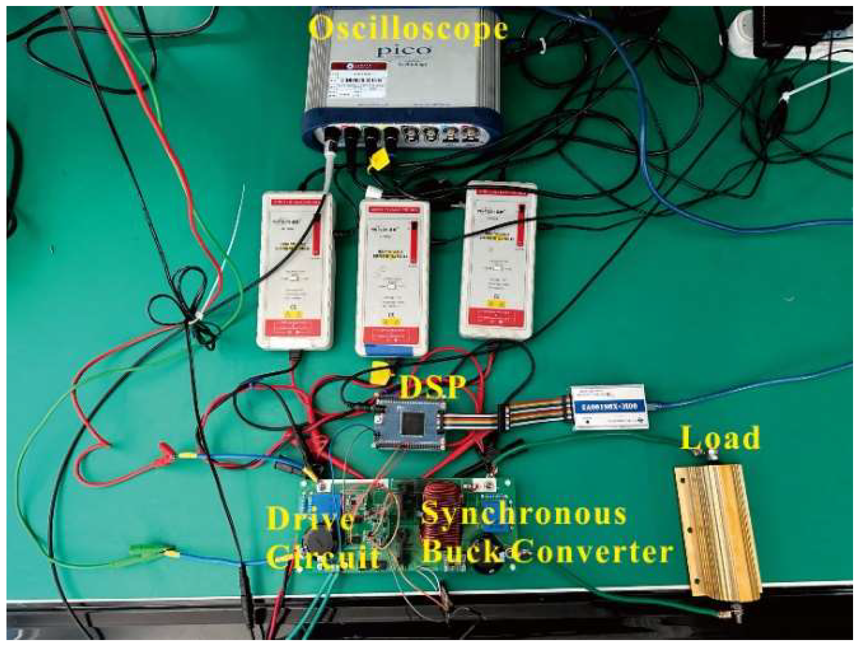
6. Experimental Verification of the Improved Crosstalk Suppression Gate Drive

In order to verify the designed improved crosstalk suppression gate drive, a synchronous buck circuit experimental platform based on SiC MOSFET is built, and the experimental scheme diagram is shown in Figure 13.
Figure 14 shows the experimental platform, which includes the driving circuit, synchronous buck converter, power supply, DSP28335, and oscilloscope. The experiment used DSP28335 to set PWM to control the driving circuit. The SiC MOSFET was CREE’s second-generation 1.2 kV SiC MOSFET semiconductor device C2M0080120D. The switching frequency was 100 KHz. The high-voltage side voltage was 300 V.
Figure 15 is the positive crosstalk voltage experimental waveform diagram; Figure 15a is the gate-source voltage waveform diagram of the upper and lower transistors Vgs, the drain-source voltage waveform diagram of the upper transistors VdsH, and the drain current waveform diagram of the upper transistors idH of three gate drives. When using the conventional gate drive, the positive crosstalk voltage is 5.68 V, and the negative crosstalk voltage is −1.73 V. When using the active clamp drive circuit, the positive crosstalk voltage is 2.38 V, and the negative crosstalk voltage is −1.62 V. When using the designed crosstalk suppression circuit, the positive crosstalk voltage is −0.15 V, and the negative crosstalk voltage is −1.14 V. At the same time, the improved drive circuit also reduces the switching time.
Figure 16 is the negative crosstalk voltage experimental waveform diagram; Figure 16a is the gate-source voltage waveform diagram of the upper and lower transistors Vgs, the drain-source voltage waveform diagram of the upper transistors VdsH, and the drain current waveform diagram of the upper transistors idH of three gate drives. When using the traditional gate drive, the positive crosstalk voltage is 2.13 V, the negative crosstalk voltage is −2.87 V, and the drain voltage peak is 411 V. When using the active clamp drive circuit, the positive crosstalk voltage is 0.47 V, the negative crosstalk voltage is −1.53 V, and the drain voltage peak is 392 V. When using the designed crosstalk suppression circuit, the positive crosstalk voltage is −0.05 V, the negative crosstalk voltage is −0.34 V, and the drain voltage peak is 375 V.
In summary, the gate drive designed in this paper has a small crosstalk voltage value that is always negative and has a significantly reduced positive and negative crosstalk voltage compared with the traditional gate drive and active clamp drive circuit.

7. Conclusions

The bridge circuit based on a SiC MOSFET is easily affected by parasitic parameters at high frequency and generates crosstalk voltage at the gate source, which greatly limits the application of the SiC MOSFET. To address this issue, a new gate drive was proposed, and it was verified by simulation and experimental methods. It can be concluded from the experimental results that the designed driver circuit compared with the traditional driver circuit can be better when the crosstalk voltage positive peak attenuation below 0 V, the maximum positive crosstalk voltage in the synchronous buck circuit test platform is −0.15 V and the negative crosstalk voltage is −0.34 V; it effectively reduces the negative crosstalk voltage, shortens the switching time of the SiC MOSFET, and reduces the drain voltage peaks. In addition, the devices used in the designed gate drive are passive devices, so the gate drive is easy to implement and does not require additional control signals; thus, the use of electronic components can be reduced. The device cost is lower than other traditional drive circuit that can be used for production.

Author Contributions

Conceptualization, methodology, and investigation, Z.G.; software, formal analysis, resources, and writing—original draft preparation, J.H.; data curation, writing—review and editing, validation, supervision, and funding acquisition, R.M. All authors have read and agreed to the published version of the manuscript.

Funding

This work was supported in part by the Natural Science Foundation of Shanxi Province under Project 20210302123170, and the National Natural Science Foundation of China (no. U1610121).

Data Availability Statement

The data are contained within the article.

Conflicts of Interest

The authors declare no conflicts of interest.

References

  1. Wu, X.; Zaman, H.; Wu, P.; Jia, R.; Zhao, X.; Wu, X. A Quasi-Multilevel Gate Driver for Fast Switching and Crosstalk Suppression of SiC Devices. IEEE Access 2020, 8, 191403–191412. [Google Scholar]
  2. Zhang, B.; Wang, S. Miller Capacitance Cancellation to Improve SiC MOSFET’s Performance in a Phase-Leg Configuration. IEEE Trans. Power Electron. 2021, 36, 14195–14206. [Google Scholar] [CrossRef]
  3. Shao, T.; Zheng, T.Q.; Li, H.; Liu, J.; Li, Z.; Huang, B.; Qiu, Z. The Active Gate Drive Based on Negative Feedback Mechanism for Fast Switching and Crosstalk Suppression of SiC Devices. IEEE Trans. Power Electron. 2022, 37, 6739–6754. [Google Scholar] [CrossRef]
  4. Li, B.; Zhang, G.; Li, C.; Wang, G.; Liu, S.; Xu, D. Crosstalk Suppression Method for GaN-Based Bridge Configuration Using Negative Voltage Self-Recovery Gate Drive. IEEE Trans. Power Electron. 2022, 37, 4406–4418. [Google Scholar] [CrossRef]
  5. Huang, Y.; Zhang, J.; Wang, Z. A Resonant Auxiliary Drive Circuit for SiC MOSFET to Suppress Crosstalk. Trans. China Electrotech. Soc. 2022, 37, 3004–3015. [Google Scholar]
  6. Li, G.; Hang, L.; Tong, A.; Zeng, Q.; He, Y. The Driver Design of SiC MOSFET With Active Crosstalk Suppression. Proc. CSEE 2021, 41, 3915–3922. [Google Scholar]
  7. Li, H.; Huang, Z.; Liao, X. An Improved SiC MOSFET Gate Driver Design for Crosstalk Suppression in a Phase-Leg Configuration. Trans. China Electrotech. Soc. 2019, 34, 275–285. [Google Scholar]
  8. Li, H.; Jiang, Y.; Qiu, Z.; Shao, T.; Wang, Y. A Multi-step Active Gate Driver for Suppressing Crosstalk of SiC MOSFET. In Proceedings of the 2020 IEEE 9th International Power Electronics and Motion Control Conference (IPEMC2020-ECCE Asia), Nanjing, China, 29 November–2 December 2020; pp. 1868–1873. [Google Scholar]
  9. Lee, G.-Y.; Ju, C.-T.; Min, S.-S.; Kim, R.-Y. Gate Driver for Wide-Bandgap Power Semiconductors With Small Negative Spike and Switching Ringing in Zero-Voltage Switching Circuit. IEEE Access 2021, 9, 145774–145784. [Google Scholar] [CrossRef]
  10. Bi, C.; Ou, H.; Kang, Q.; Li, R.; Cheng, L. A Novel Driver Circuit on Crosstalk Suppression in SiC MOSFETs. In Proceedings of the 2021 IEEE International Symposium on Circuits and Systems (ISCAS), Daegu, Republic of Korea, 22–28 May 2021; pp. 1–5. [Google Scholar]
  11. Lu, Z.; Li, C.; Wu, H.; Li, W.; He, X.; Li, S. Design of Active SiC MOSFET Gate Driver for Crosstalk Suppression Considering Impedance Coordination between Gate Loop and Power Loop. In Proceedings of the 2019 IEEE Applied Power Electronics Conference and Exposition (APEC), Anaheim, CA, USA, 17–21 March 2019; pp. 986–990. [Google Scholar]
  12. Li, H.; Jiang, Y.; Qiu, Z.; Wang, Y.; Ding, Y. A Predictive Algorithm for Crosstalk Peaks of SiC MOSFET by Considering the Nonlinearity of Gate-Drain Capacitance. IEEE Trans. Power Electron. 2021, 36, 2823–2834. [Google Scholar] [CrossRef]
  13. Liang, M.; Li, Y.; Zheng, Q.; Zhao, H. Analysis for Crosstalk of SiC MOSFET with Different Packages in a Phase-Leg Configuration and a Low Gate Turn-Off Impedance Driver. Trans. China Electrotech. Soc. 2017, 32, 162–174. [Google Scholar]
  14. Zhang, Z.; Wang, F.; Tolbert, L.M.; Blalock, B.J. Active Gate Driver for Crosstalk Suppression of SiC Devices in a Phase-Leg Configuration. IEEE Trans. Power Electron. 2014, 29, 1986–1997. [Google Scholar] [CrossRef]
  15. Zhao, J.; Wu, L.; Li, Z.; Chen, Z.; Chen, G. Analysis and Suppression for Crosstalk in SiC MOSFET Turn-off Transient. In Proceedings of the 2020 IEEE 9th International Power Electronics and Motion Control Conference (IPEMC2020-ECCE Asia), Nanjing, China, 29 November–2 December 2020; pp. 1145–1150. [Google Scholar]
  16. Wang, J.; Chung, H.S.-H. A Novel RCD Level Shifter for Elimination of Spurious Turn-on in the Bridge-Leg Configuration. IEEE Trans. Power Electron. 2015, 30, 976–984. [Google Scholar] [CrossRef]
  17. Wang, P.; Zhang, L.; Lu, X.; Sun, H.; Wang, W.; Xu, D. An Improved Active Crosstalk Suppression Method for High-Speed SiC MOSFETs. IEEE Trans. Ind. Appl. 2019, 55, 7736–7744. [Google Scholar] [CrossRef]
  18. Gao, F.; Zhou, Q.; Wang, P.; Zhang, C. A Gate Driver of SiC MOSFET for Suppressing the Negative Voltage Spikes in a Bridge Circuit. IEEE Trans. Power Electron. 2017, 33, 2339–2353. [Google Scholar] [CrossRef]
  19. Zhang, B.; Wang, S. A crosstalk suppression technique for SiC MOSFETs in the bridge-leg configuration. In Proceedings of the 2020 IEEE Applied Power Electronics Conference and Exposition (APEC), New Orleans, LA, USA, 15–19 March 2020; pp. 1513–1520. [Google Scholar]
  20. Tang, B.H.-T.; Chung, H.S.-H.; Fan, J.W.-T.; Yeung, R.S.-C. Passive Resonant Level Shifter for Suppression of Crosstalk Effect and Reduction of Body-Diode Loss in SiC-Based Bridge Leg. In Proceedings of the 2018 IEEE Energy Conversion Congress and Exposition (ECCE), Portland, OR, USA, 23–27 September 2018; pp. 3510–3516. [Google Scholar]
  21. Xu, Y.; Duan, B.; Song, J.; Yang, D.; Zhang, C. A Novel Gate Driver of SiC MOSFET for Crosstalk Suppression in Bridge Configuration. In Proceedings of the 2020 Chinese Automation Congress (CAC), Shanghai, China, 6–8 November 2020; pp. 1173–1178. [Google Scholar]
  22. Li, G.; Tong, A.; Hang, L.; Zeng, Q.; Zhan, X.; Li, G.; He, Y.; Xie, X.; Shen, L.; Zhang, Y. A Level Shift Gate Driving Circuit of SiC MOSFET with Crosstalk Suppression Capability. In Proceedings of the 2020 IEEE Applied Power Electronics Conference and Exposition (APEC), New Orleans, LA, USA, 15–19 March 2020; pp. 1806–1812. [Google Scholar]
  23. Zhang, Z.; Wang, F.; Tolbert, L.M.; Blalock, B.J. A gate assist circuit for cross talk suppression of SiC devices in a phase-leg configuration. In Proceedings of the 2013 IEEE Energy Conversion Congress and Exposition, Denver, CO, USA, 15–19 September 2013; pp. 2536–2543. [Google Scholar]
  24. Zhang, B.; Xie, S.; Xu, J.; Qian, Q.; Zhang, Z.; Xu, K. A Magnetic Coupling Based Gate Driver for Crosstalk Suppression of SiC MOSFETs. IEEE Trans. Ind. Electron. 2017, 64, 9052–9063. [Google Scholar] [CrossRef]
Figure 1. Crosstalk voltage generation mechanism: (a) positive crosstalk voltage generation mechanism; (b) negative crosstalk voltage generation mechanism.
Electronics 13 02922 g001
Figure 2. Improved crosstalk suppression gate drive.
Electronics 13 02922 g002
Figure 3. The switch waveform of the relevant variables of the improved gate drive.
Electronics 13 02922 g003
Figure 4. Operation mode diagram of the improved gate drive: (a) Mode 1; (b) Mode 2; (c) Mode 3; (d) Mode 4; (e) Mode 5; (f) Mode 6; (g) Mode 7; (h) Mode 8.
Electronics 13 02922 g004aElectronics 13 02922 g004b
Figure 5. Schematic diagram of pre-charging.
Electronics 13 02922 g005
Figure 6. Equivalent circuit for pre-charging.
Electronics 13 02922 g006
Figure 7. The equivalent circuit when the auxiliary branch is not connected to the gate drive.
Electronics 13 02922 g007
Figure 8. The equivalent circuit when the auxiliary branch is connected to the gate drive.
Electronics 13 02922 g008
Figure 9. Driver circuit simulation model: (a) no-crosstalk suppression drive circuit; (b) active clamp drive circuit; (c) improved crosstalk suppression.
Electronics 13 02922 g009
Figure 10. Positive crosstalk voltage simulation waveform diagram: (a) control transistors; (b) synchronous transistor.
Electronics 13 02922 g010
Figure 11. Negative crosstalk voltage simulation waveform diagram: (a) control transistors; (b) synchronous transistor.
Electronics 13 02922 g011
Figure 12. Switching loss comparison diagram of the lower switching transistor: (a) on; (b)off.
Electronics 13 02922 g012
Figure 13. Synchronous buck circuit experimental model.
Electronics 13 02922 g013
Figure 14. Synchronous buck circuit experimental platform.
Electronics 13 02922 g014
Figure 15. Positive crosstalk voltage experimental waveform diagram: (a) conventional gate drive; (b) active clamp drive circuit; (c) improved crosstalk suppression.
Electronics 13 02922 g015
Figure 16. Negative crosstalk voltage experimental waveform diagram: (a) conventional gate drive; (b) active clamp drive circuit; (c) improved crosstalk suppression.
Electronics 13 02922 g016
Table 1. Basic parameters of the SiC MOSFET.
ParametersValue
Gate-source capacitance Cgs1092 pF
Gate-drain capacitance Cgd8 pF
Drain-source capacitance Cds92 pF
Threshold voltage Vth3 V
Max negative gate-source voltage VMAX(neg)−10 V
Internal gate resistance Rg(in) 3.8   Ω
Table 2. Gate drive parameters list.
SymbolValue
C1_n100 pF
C2_n100 pF
R1_n 1000   Ω
R2_n 4700   Ω
R3_n 10   Ω
Disclaimer/Publisher’s Note: The statements, opinions and data contained in all publications are solely those of the individual author(s) and contributor(s) and not of MDPI and/or the editor(s). MDPI and/or the editor(s) disclaim responsibility for any injury to people or property resulting from any ideas, methods, instructions or products referred to in the content.

