

A Configurable Resolution Time-to-Digital Converter with Low PVT Sensitivity for LiDAR Applications

Abstract
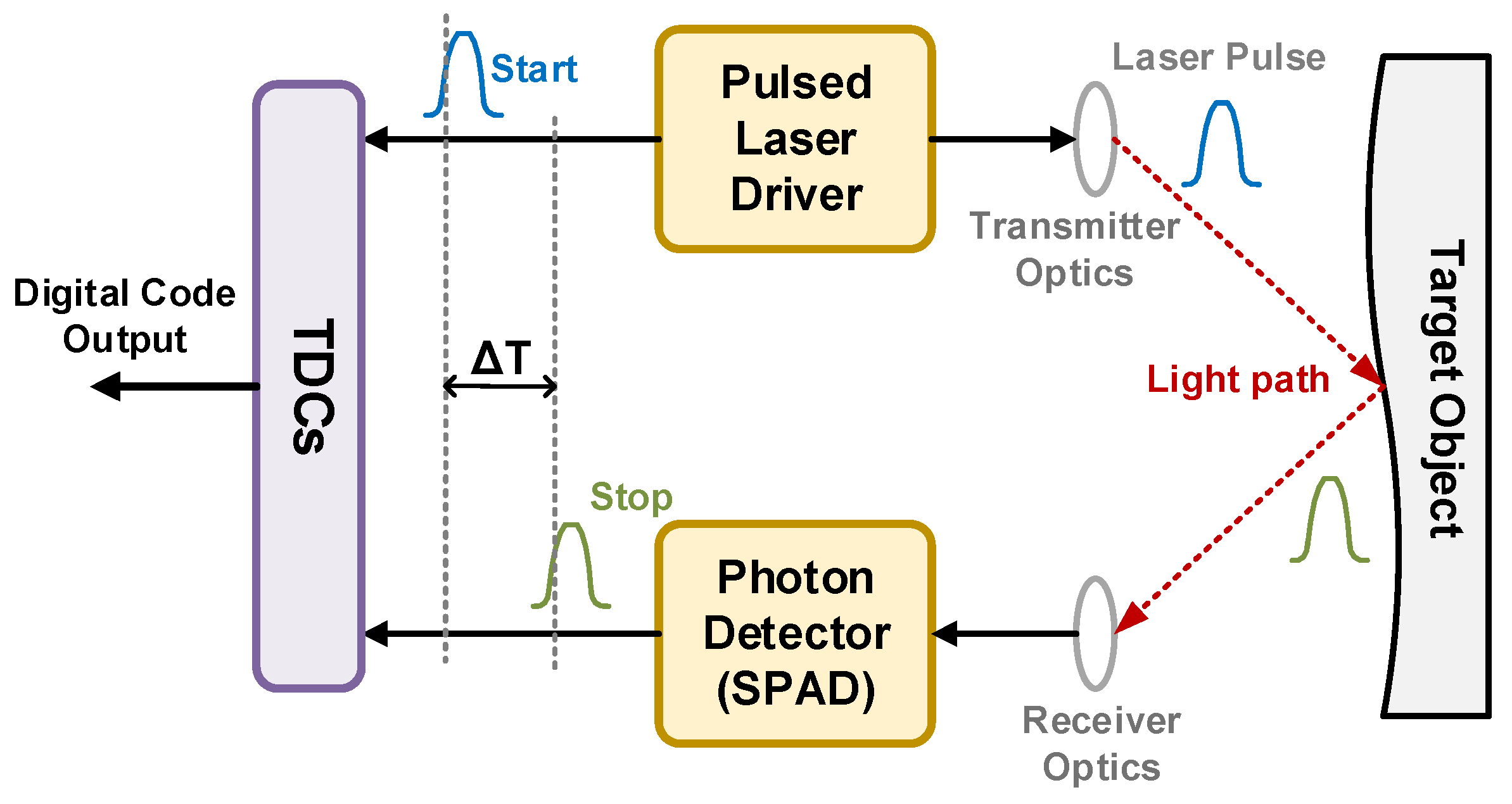
:1. Introduction
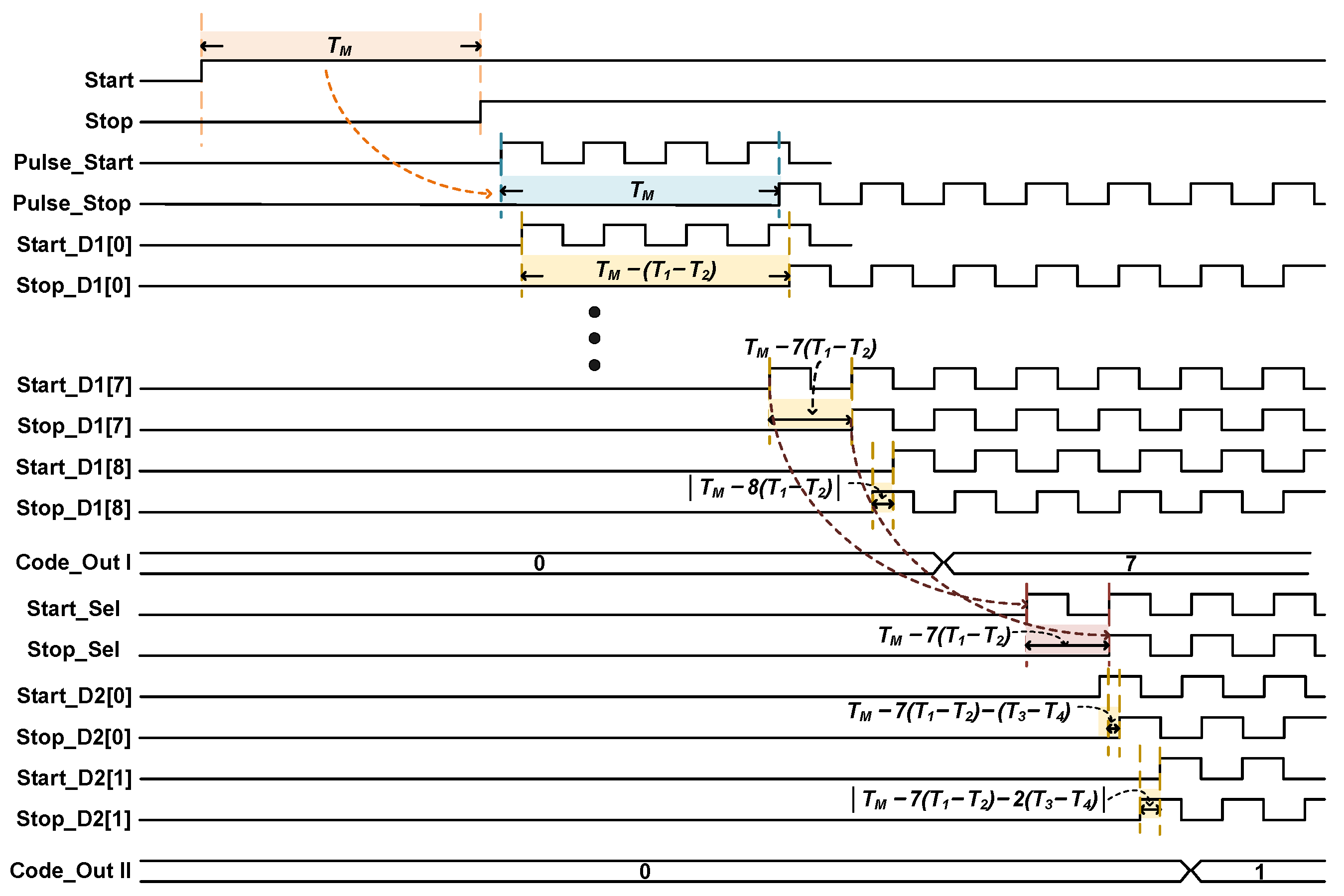
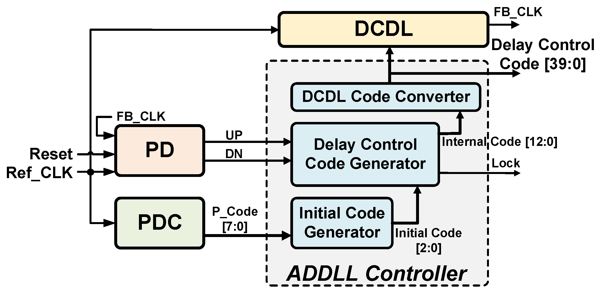
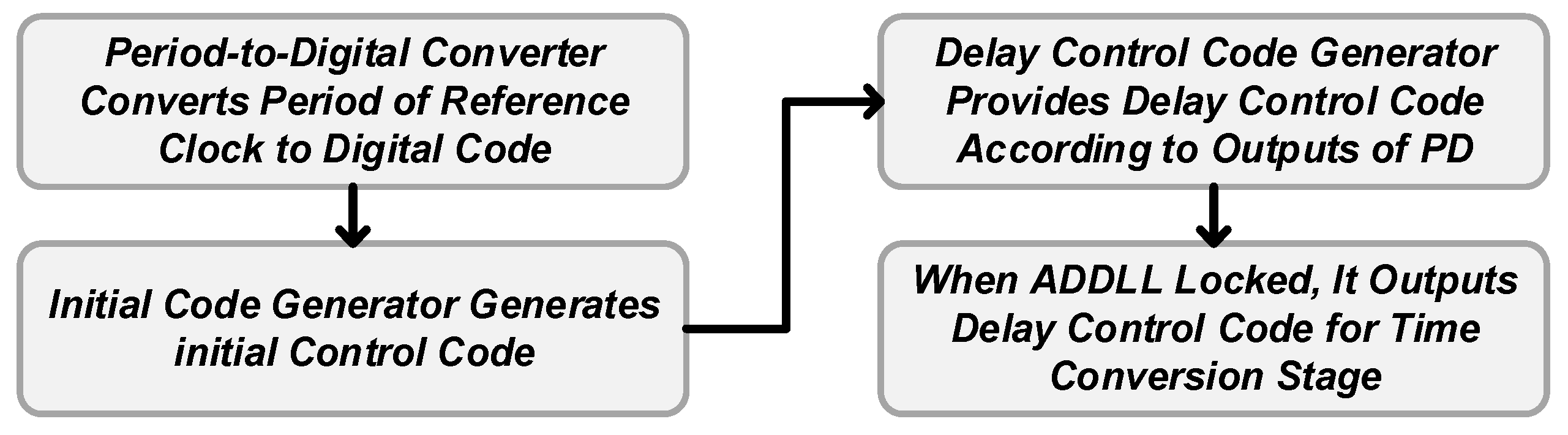
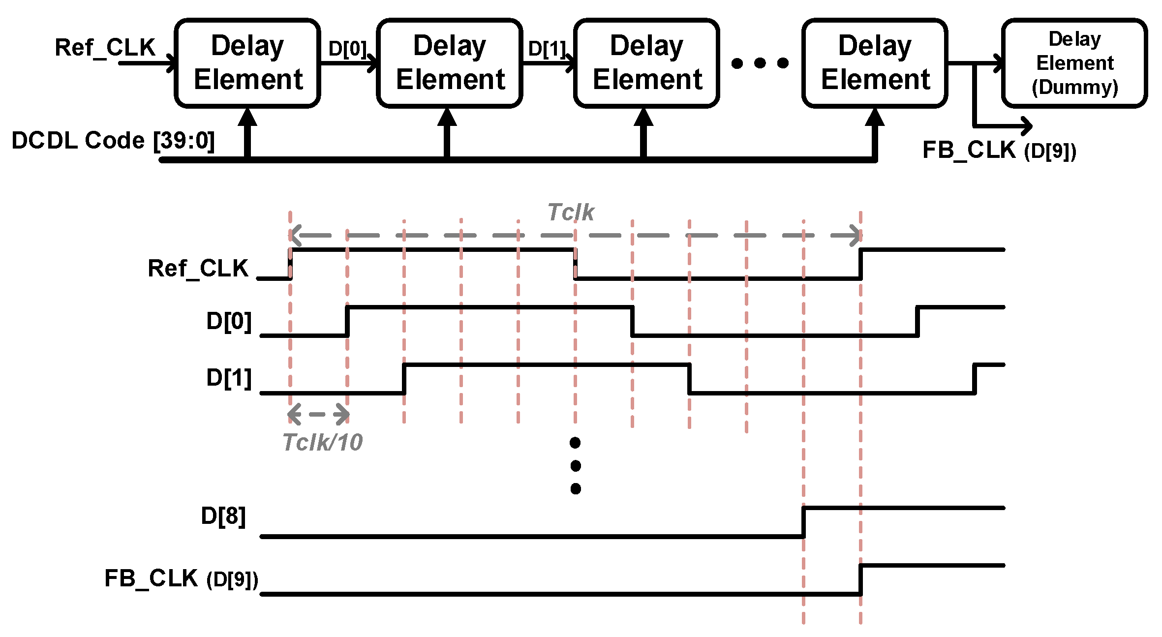
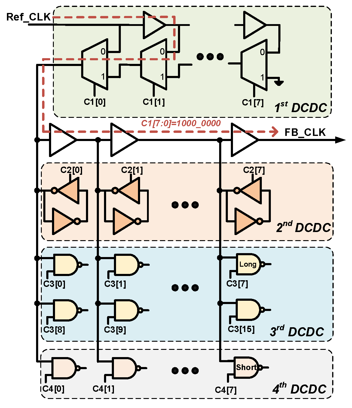
2. TDC Architecture Overview
3. Circuit Design
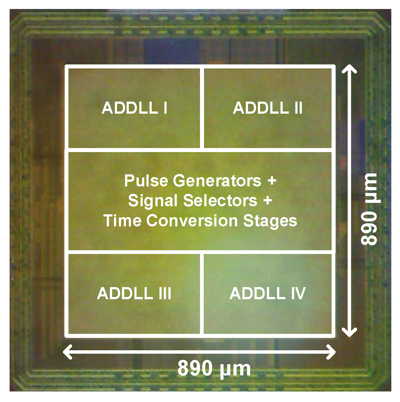
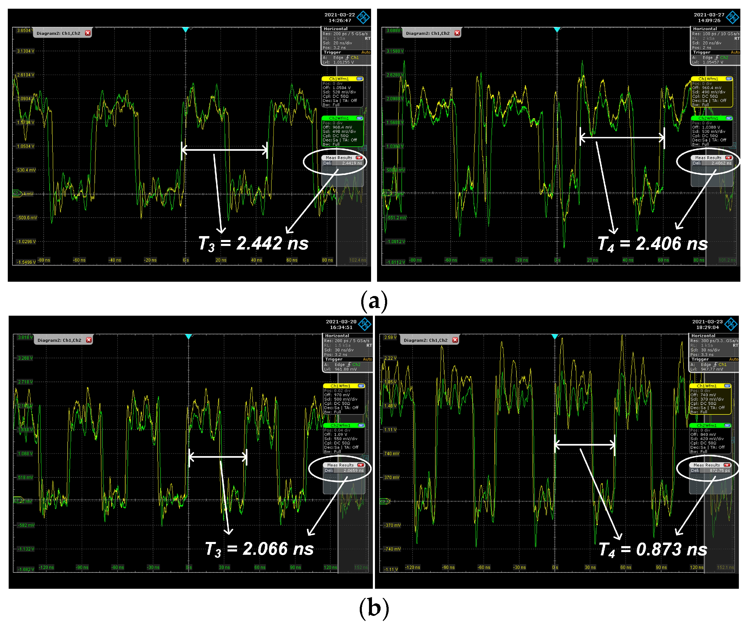
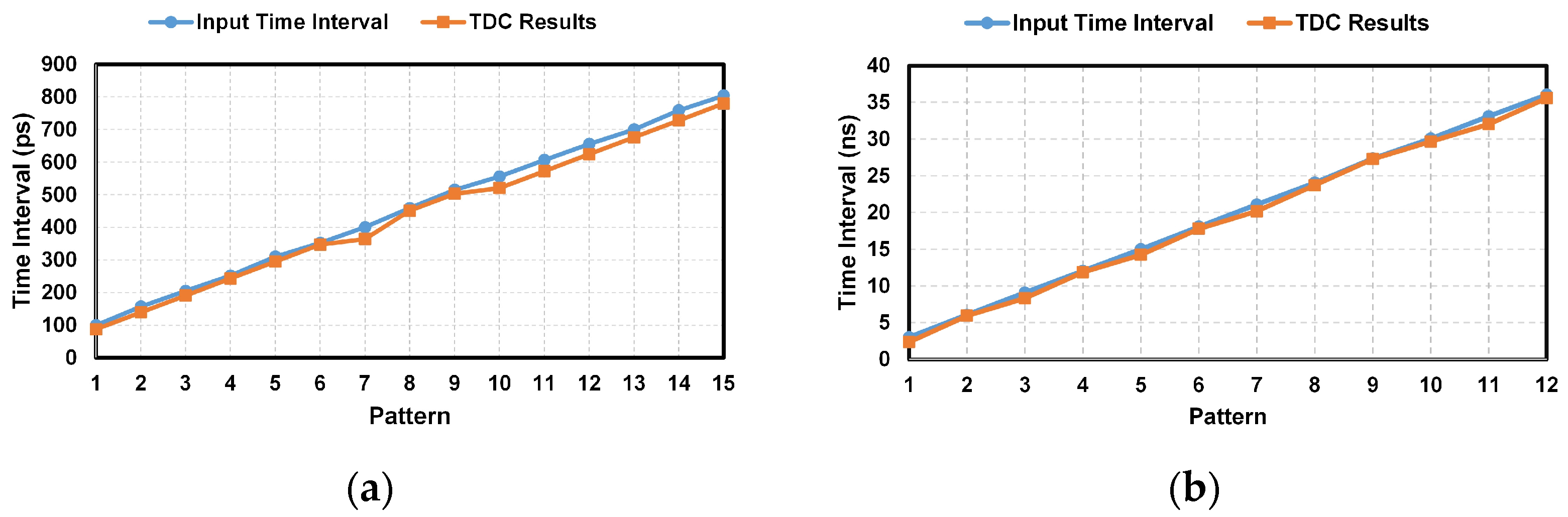
4. Experimental Results
5. Conclusions
Author Contributions
Funding
Data Availability Statement
Acknowledgments
Conflicts of Interest
References
- Cova, S.; Bertolaccini, M.; Bussolati, C. The measurement of luminescence waveforms by single-photon techniques. Phys. Status Solidi 1973, 18, 11–62. [Google Scholar] [CrossRef]
- Tamborini, D.; Buttafava, M.; Ruggeri, A.; Zappa, F. Compact, low-power and fully reconfigurable 10 ps resolution, 160 μs range, time-resolved single-photon counting system. IEEE Sens. J. 2016, 16, 3827–3833. [Google Scholar] [CrossRef]
- Seo, M.W.; Kagawa, K.; Yasutomi, K.; Kawata, Y.; Teranishi, N.; Li, Z.; Halin, R.A.; Kawahito, S. A 10 ps time-resolution CMOS image sensor with two-tap true-CDS lock-in pixels for fluorescence lifetime imaging. IEEE J. Solid-State Circuits 2016, 51, 141–154. [Google Scholar] [CrossRef]
- Niclass, C.; Soga, M.; Matsubara, H.; Kato, S.; Kagami, M. A 100-m range 10-frame/s 340 × 96-pixel time-off-flight depth sensor in 0.18-µm CMOS. IEEE J. Solid-State Circuits 2013, 48, 559–572. [Google Scholar] [CrossRef]
- Niclass, C.; Soga, M.; Matsubara, H.; Ogawa, M.; Kagami, M. A 0.18-µm CMOS SoC for a 100-m-range 10-frame/s 200 × 96-Pixel time-of-flight depth sensor. IEEE J. Solid-State Circuits 2014, 49, 315–330. [Google Scholar] [CrossRef]
- Zhang, C.; Lindner, S.; Antolović, I.M.; Pavia, J.M.; Wolf, M.; Charbon, E. A 30-frames/s, 252 × 144 SPAD flash LiDAR with 1728 dual-clock 48.8-ps TDCs, and pixel-wise integrated histogramming. IEEE J. Solid-State Circuits 2019, 54, 1137–1151. [Google Scholar] [CrossRef]
- Seo, H.; Yoon, S.; Kim, D.; Kim, J.; Kim, S.-J.; Chun, J.-H.; Choi, J. Direct TOF scanning LiDAR sensor with two-step multievent histogramming TDC and embedded interference Filter. IEEE J. Solid-State Circuits 2021, 56, 1022–1035. [Google Scholar] [CrossRef]
- Perenzoni, M.; Perenzoni, D.; Stoppa, D. A 64 × 64-Pixels digital silicon photomultiplier direct TOF sensor with 100-MPhotons/s/pixel background rejection and imaging/altimeter mode with 0.14% precision up to 6 km for spacecraft navigation and landing. IEEE J. Solid-State Circuits 2017, 52, 151–160. [Google Scholar] [CrossRef]
- Zhang, W.; Ma, R.; Wang, X.; Zheng, H.; Zhu, Z. A High Linearity TDC With a United-Reference Fractional Counter for LiDAR. IEEE Trans. Circuits Syst. I Regul. Pap. 2022, 69, 564–572. [Google Scholar] [CrossRef]
- Arvani, F.; Carusone, T.C. A reconfigurable 5-channel ring-oscillator-based TDC for direct time-of-flight 3D imaging. IEEE Trans. Circuits Syst. II Express Briefs 2022, 69, 2408–2412. [Google Scholar] [CrossRef]
- Hu, J.; Li, D.; Wang, X.; Ma, R.; Liu, Y.; Zhu, Z. A 40-ps resolution robust continuous running VCRO-based TDC for LiDAR applications. IEEE Trans. Circuits Syst. II Express Briefs 2023, 70, 426–430. [Google Scholar] [CrossRef]
- Arvani, F.; Carusone, A.C. Peak-SNR analysis of CMOS TDCs for SPAD-based TCSPC 3D imaging applications. IEEE Trans. Circuits Syst. II Express Briefs 2023, 70, 426–430. [Google Scholar] [CrossRef]
- Cheng, Z.; Zheng, X.; Deen, M.J.; Peng, H. Recent developments and design challenges of high-performance ring oscillator CMOS time-to-digital converters. IEEE Trans. Electron Devices 2016, 63, 235–251. [Google Scholar] [CrossRef]
- Cheng, C.C.; Hou, C.-Y. An all-digital delay-locked loop for 3-D ICs die-to-die clock deskew applications. Microelectron. J. 2017, 70, 63–71. [Google Scholar] [CrossRef]
- Sheng, D.; Cheng, C.-C.; Lee, C.-Y. An ultra-low-power and portable digitally controlled oscillator for SoC applications. IEEE Trans. Circuits Syst. II Express Briefs 2007, 54, 954–958. [Google Scholar] [CrossRef]


| 1st DCDC | 2nd DCDC | 3rd DCDC | 4th DCDC | |
|---|---|---|---|---|
| Range (ps) | 1595.2 | 578.5 | 223.4 | 26.3 |
| Resolution (ps) | 227.8 | 82.6 | 14.8 | 3.76 |
| Performance Indices | Proposed | [11] | [6] | [4] |
|---|---|---|---|---|
| Process | 0.18 μm CMOS | 0.18 μm CMOS | 0.18 μm CMOS | 0.18 μm CMOS |
| Resolution (ps) | 36~1190 | 40 | 48.8 | 208 |
| Range (μs) | 0.1~36 | N/A | 50 | N/A |
| Number of Bits | 7 | 11 | 12 | 12 |
| Configurable Resolution | Yes | No | No | No |
| Power Consumption (mW) | 28.4 | 2.19 | 0.3 | N/A |
| Area | 0.79 mm2 | 1350 μm2 | 4200 μm2 | N/A |
| PVT Sensitivity | Low | Low | High | High |
Disclaimer/Publisher’s Note: The statements, opinions and data contained in all publications are solely those of the individual author(s) and contributor(s) and not of MDPI and/or the editor(s). MDPI and/or the editor(s) disclaim responsibility for any injury to people or property resulting from any ideas, methods, instructions or products referred to in the content. |
© 2024 by the authors. Licensee MDPI, Basel, Switzerland. This article is an open access article distributed under the terms and conditions of the Creative Commons Attribution (CC BY) license (https://creativecommons.org/licenses/by/4.0/).
Share and Cite
Sheng, D.; Huang, H.-T.; Liu, R.-L.; Cheng, C.-I.; Wang, X.-T. A Configurable Resolution Time-to-Digital Converter with Low PVT Sensitivity for LiDAR Applications. Electronics 2024, 13, 2923. https://doi.org/10.3390/electronics13152923
Sheng D, Huang H-T, Liu R-L, Cheng C-I, Wang X-T. A Configurable Resolution Time-to-Digital Converter with Low PVT Sensitivity for LiDAR Applications. Electronics. 2024; 13(15):2923. https://doi.org/10.3390/electronics13152923
Chicago/Turabian StyleSheng, Duo, Hao-Ting Huang, Ruey-Lin Liu, Cheng-I Cheng, and Xiao-Ti Wang. 2024. "A Configurable Resolution Time-to-Digital Converter with Low PVT Sensitivity for LiDAR Applications" Electronics 13, no. 15: 2923. https://doi.org/10.3390/electronics13152923